Light emitting transistor
US20080116465A1
2008-05-22
11/878,680
2007-07-26
✅ Patent granted
US 7,675,071 B2
2010-03-09
-
-
Dao H Nguyen | Tram H Nguyen
2027-11-27
Abstract:
Provided is a light emitting transistor comprising a first conductivity-type collector layer formed on a substrate; a second conductivity-type base layer formed on the collector layer; and a first conductivity-type emitter layer formed on the base layer. At least one of the collector layer, the base layer, and the emitter layer has a nanorod structure with a plurality of nanorods.
Inventors:
- Hyun Jun KIM 21 🇰🇷 Suwon, South Korea
- Chang Hwan Choi 12 🇰🇷 Seongnam, South Korea
- Won Ha MOON 14 🇰🇷 Suwon, South Korea
Assignee:
- SAMSUNG ELECTRO-MECHANICS CO., LTD. 1,460 🇰🇷 Gyunggi-do, South Korea
Interested in similar patents?
Get notified when new applications in this technology area are published.
Classification:
H01L33/0004 » CPC main
Semiconductor devices with at least one potential-jump barrier or surface barrier specially adapted for light emission; Processes or apparatus specially adapted for the manufacture or treatment thereof or of parts thereof; Details thereof Devices characterised by their operation
B82Y20/00 » CPC further
Nanooptics, e.g. quantum optics or photonic crystals
H01L33/08 » CPC further
Semiconductor devices with at least one potential-jump barrier or surface barrier specially adapted for light emission; Processes or apparatus specially adapted for the manufacture or treatment thereof or of parts thereof; Details thereof characterised by the semiconductor bodies with a plurality of light emitting regions, e.g. laterally discontinuous light emitting layer or photoluminescent region integrated within the semiconductor body
H01L33/18 » CPC further
Semiconductor devices with at least one potential-jump barrier or surface barrier specially adapted for light emission; Processes or apparatus specially adapted for the manufacture or treatment thereof or of parts thereof; Details thereof characterised by the semiconductor bodies with a particular crystal structure or orientation, e.g. polycrystalline, amorphous or porous within the light emitting region
H01L33/20 » CPC further
Semiconductor devices with at least one potential-jump barrier or surface barrier specially adapted for light emission; Processes or apparatus specially adapted for the manufacture or treatment thereof or of parts thereof; Details thereof characterised by the semiconductor bodies with a particular shape, e.g. curved or truncated substrate
H01L27/15 IPC
Devices consisting of a plurality of semiconductor or other solid-state components formed in or on a common substrate including semiconductor components with at least one potential-jump barrier or surface barrier specially adapted for light emission
H01L29/26 IPC
Semiconductor devices adapted for rectifying, amplifying, oscillating or switching, or capacitors or resistors with at least one potential-jump barrier or surface barrier, e.g. PN junction depletion layer or carrier concentration layer; Details of semiconductor bodies or of electrodes thereof; Multistep manufacturing processes therefor; Semiconductor bodies ; Multistep manufacturing processes therefor characterised by the materials of which they are formed including, apart from doping materials or other impurities, elements provided for in two or more of the groups , , , , , e.g. alloys
H01L31/12 IPC
Semiconductor devices sensitive to infra-red radiation, light, electromagnetic radiation of shorter wavelength or corpuscular radiation and specially adapted either for the conversion of the energy of such radiation into electrical energy or for the control of electrical energy by such radiation; Processes or apparatus specially adapted for the manufacture or treatment thereof or of parts thereof; Details thereof structurally associated with, e.g. formed in or on a common substrate with, one or more electric light sources, e.g. electroluminescent light sources, and electrically or optically coupled thereto
H01L33/00 IPC
Semiconductor devices with at least one potential-jump barrier or surface barrier specially adapted for light emission; Processes or apparatus specially adapted for the manufacture or treatment thereof or of parts thereof; Details thereof
Description
CROSS-REFERENCE TO RELATED APPLICATIONS
This application claims the benefit of Korean Patent Application No. 10-2006-0113886 filed with the Korean Intellectual Property Office on Nov. 17, 2005, the disclosure of which is incorporated herein by reference.
BACKGROUND OF THE INVENTION
1. Field of the Invention
The present invention relates to a light emitting transistor with a nano structure which can amplify and switch optical and electrical characteristics.
2. Description of the Related Art
In general, a light emitting diode (LED) generates minority carriers (electrons or holes) injected by using the p-n junction structure of a semiconductor, and recombines the minority carriers so as to emit light. In other words, if a forward voltage is applied to a specific element of semiconductor, electrons and holes are recombined while moving through the junction between an anode and a cathode. Since energy in such a state is smaller than energy in a state where the electrons and holes are separated, light is emitted due to a difference in energy occurring at this time.
Such an LED can irradiate light with high efficiency by using a low voltage. Therefore, the LED is used in a home appliance, a remote control, an electronic display board, a marker, an automation equipment and the like.
Meanwhile, most of semiconductor electronic elements are implemented with transistors, and transistors formed of group III-V and II-VI nitride semiconductors are manufactured and are used in various fields.
However, researches about transistors for light emission have almost never carried out. In this technical field, a new method for amplifying and switching optical and electrical characteristics is being required.
SUMMARY OF THE INVENTION
An advantage of the present invention is that it provides a light emitting transistor with a nano structure which can amplify and switch optical and electrical characteristics.
Additional aspect and advantages of the present general inventive concept will be set forth in part in the description which follows and, in part, will be obvious from the description, or may be learned by practice of the general inventive concept.
According to an aspect of the invention, a light emitting transistor comprises a first conductivity-type collector layer formed on a substrate; a second conductivity-type base layer formed on the collector layer; and a first conductivity-type emitter layer formed on the base layer. At least one of the collector layer, the base layer, and the emitter layer has a nanorod structure with a plurality of nanorods.
The first conductivity type may n-type, and the second conductivity type may be p-type. Alternately, the first conductivity type may be p-type, and the second conductivity type may be n-type.
Preferably, the collector layer, the base layer, and the emitter layer are formed of group II-VI or II-V compound semiconductors.
Preferably, the light emitting transistor further comprises an activation layer formed at the interface between the collector layer and the base layer or at the interface between the base layer and the emitter layer.
Preferably, the activation layer has a nanorod structure with a plurality of nanorods and is formed of a group II-VI or II-V compound semiconductor.
BRIEF DESCRIPTION OF THE DRAWINGS
These and/or other aspects and advantages of the present general inventive concept will become apparent and more readily appreciated from the following description of the embodiments, taken in conjunction with the accompanying drawings of which:
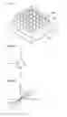
FIG. 1 is a perspective view illustrating the structure of a light emitting transistor according to an embodiment of the invention;
FIG. 2A is a diagram showing an equivalent circuit of the light emitting transistor according to an embodiment of the invention;
FIG. 2B is a diagram showing an I-V curve of the light emitting transistor; and
FIGS. 3 to 8 are perspective views illustrating modifications of the light emitting transistor according to an embodiment of the invention.
DETAILED DESCRIPTION OF THE PREFERRED EMBODIMENTS
Reference will now be made in detail to the embodiments of the present general inventive concept, examples of which are illustrated in the accompanying drawings, wherein like reference numerals refer to like elements throughout. The embodiments are described below in order to explain the present general inventive concept by referring to the figures. In the drawings, the thicknesses of layers and regions are exaggerated for clarity.
Hereinafter, a light emitting transistor according to an embodiment of the present invention will be described in detail with reference to the accompanying drawings.
FIG. 1 is a perspective view illustrating the structure of a light emitting transistor according to an embodiment of the invention.
As shown in FIG. 1, the light emitting transistor according to the invention basically has a bipolar junction structure.
That is, the light emitting transistor includes a substrate 100, a first conductivity-type collector layer 110 formed on the substrate, a second conductive-type base layer 120 formed on the collector layer 110, and a first conductivity-type emitter layer 130 formed on the base layer 120, the first conductivity-type emitter layer 130 having the same conductivity type as the first conductivity-type collector layer 110.
The collector layer 110, the base layer 120, and the emitter layer 130 may be formed of group II-VI or III-V compound semiconductors. As for the group II-VI compound semiconductors, ZnSe, ZnTe, ZnSeTe, ZnS, ZnO, CdSe, CdS, CdTe, ZnCdS, ZnCdSe, ZnCdSeTe, ZnCdSTe and the like can be used. As for the group III-V compound semiconductors, GaAs, GaAlAs, GaInAs, InAs, InP, InSb, GaSb, GaInSb, GaN, GaInN and the like can be used.
The first conductivity type is n-type, and the second conductivity type is p-type. The collector layer 110 and the emitter layer 130 may be formed of n-type semiconductors, and the base layer 120 may be formed of a p-type semiconductor. The n-type semiconductor may be doped with Si, Se, Sn or the like, and the p-type semiconductor may be doped with Mg, Zn, Be or the like.
On the contrary, the first conductivity type may be p-type, and the second conductivity type may be n-type. Further, the collector layer 110 and the emitter layer 130 may be formed of p-type semiconductors, and the base layer 120 may be formed of an n-type semiconductor.
The emitter layer 130 is a region to which holes or electrons are injected, the collector layer 110 is a region in which the injected holes or electrons are focused, and the base layer 120 is an intermediate region between the emitter layer 130 and the collector layer 110.
At least one of the collector layer 110, the base layer 120, and the emitter layer 130 has a nanorod structure with a plurality of nanorods.
As such, when at least one of the collector layer 110, the base layer 120, and the emitter layer 130 has a nanorod structure, which is a low-dimensional nano-structure such as a quantum point and a quantum well, electrons within the nanorod structure can be effectively captured, and light emission efficiency by recombination can be enhanced.
FIG. 1 shows a state where the emitter layer 130 among the collector layer 110, the base layer 120, and the emitter layer 130 has a nanorod structure with a plurality of nanorods.
FIGS. 3 to 8 are perspective views illustrating modifications of the light emitting transistor according to an embodiment of the invention. FIG. 3 shows a state where the base layer 120 among the collector layer 110, the base layer 120, and the emitter layer 130 has a nanorod structure with a plurality of nanorods. FIG. 4 shows a state where the collector layer 110 among the collector layer 110, the base layer 120, and the emitter layer 130 has a nanorod structure with a plurality of nanorods. FIG. 5 shows a state where the collector layer 110 and the emitter layer 130 among the collector layer 110, the base layer 120, and the emitter layer 130 has a nanorod structure with a plurality of nanorods. FIG. 6 shows a state where the base layer 120 and the emitter layer 130 among the collector layer 110, the base layer 120, and the emitter layer 130 have a nanorod structure with a plurality of nanorods. FIG. 7 shows a state where the collector layer 110 and the base layer 120 among the collector layer 110, the base layer 120, and the emitter layer 130 have a nanorod structure with a plurality of nanorods. FIG. 8 shows a state where all of the collector layer 110, the base layer 120, and the emitter layer 130 have a nanorod structure with a plurality of nanorods.
Although not shown, the light emitting transistor according to the invention further includes an activation layer formed at the interface between the collector layer 110 and the base layer 120 or between the base layer 120 and the emitter layer 130. That is, the activation layer may be formed at the interface between the collector layer 110 and the base layer 120 and at the interface between the base layer 120 and the emitter layer 130. Alternately, the activation layer may be formed only at the interface between the collector layer 110 and the base layer 120 or only at the interface between the base layer 120 and the emitter layer 130. The activation layer as well as the collector layer 110, the base layer 120, and the emitter layer 130 may be formed of group II-VI or III-V compound semiconductors.
FIG. 2A is a diagram showing an equivalent circuit of the light emitting transistor according to an embodiment of the invention, and FIG. 2B is a diagram showing an I-V curve of the light emitting transistor.
Referring to FIGS. 2A and 2B, the light emitting transistor including three terminals of a collector C, a base B, and an emitter E can adjust the intensity of light generated from the activation layer by the adjustment of the base B, and the magnitude of a collector current is adjusted by a base voltage.
That is, carriers flowing in the emitter E and the collector C are electrons and holes. When a voltage is applied to the base B, the barrier of the base B is reduced in height such that carriers easily move from the emitter E to the collector C. Then, a current flowing in the collector C is amplified.
As described above, the light emitting transistor according to the invention has a bipolar junction structure including the collector layer 110, the base layer 120, and the emitter layer 130. Further, at least one of the collector layer 110, the base layer 120, and the emitter layer 130 is formed with a nanorod structure with a plurality of nanorods. Therefore, an optical and electrical output can be amplified or can be switched from on-state to off-state or from off-state to on-state, in accordance with the bias direction of each terminal.
According to the invention, the light emitting transistor has a bipolar junction structure including the collector layer, the base layer, and the emitter layer. Further, at least one of the collector layer, the base layer, and the emitter layer is formed with a nanorod structure with a plurality of nanorods. Therefore, it is possible to obtain optical and electrical characteristics at the same time.
Further, the intensity of light can be adjusted by the adjustment of the base terminal, and an optical and electrical output can be amplified or can be switched from on-state to off-state or from off-state to on-state, in accordance with the bias direction of each terminal.
Although a few embodiments of the present general inventive concept have been shown and described, it will be appreciated by those skilled in the art that changes may be made in these embodiments without departing from the principles and spirit of the general inventive concept, the scope of which is defined in the appended claims and their equivalents.
Claims
What is claimed is:1. A light emitting transistor comprising:
a first conductivity-type collector layer formed on a substrate;
a second conductivity-type base layer formed on the collector layer; and
a first conductivity-type emitter layer formed on the base layer,
wherein at least one of the collector layer, the base layer, and the emitter layer has a nanorod structure with a plurality of nanorods.
2. The light emitting transistor according to claim 1
wherein the first conductivity type is n-type, and the second conductivity type is p-type.
3. The light emitting transistor according to claim 1,
wherein the first conductivity type is p-type, and the second conductivity type is n-type.
4. The light emitting transistor according to claim 1,
wherein the collector layer, the base layer, and the emitter layer are formed of group II-VI or III-V compound semiconductors.
5. The light emitting transistor according to claim 1 further comprising
an activation layer formed at the interface between the collector layer and the base layer.
6. The light emitting transistor according to claim 1 further comprising
an activation layer formed at the interface between the base layer and the emitter layer.
7. The light emitting transistor according to claim 5,
wherein the activation layer has a nanorod structure with a plurality of nanorods.
8. The light emitting transistor according to claim 7,
wherein the activation layer is formed of a group II-VI or II-V compound semiconductor.
Images & Drawings included:


Sources:
- United States Patent and Trademark Office - verify current appl. status at the USPTO↗
Similar patent applications:
- » 20090230384
Vertical organic light emitting transistor assembly and horizontal organic light emitting transistor assembly - » 20150155430
Devices, structures, materials and methods for vertical light emitting transistors and light emitting displays - » 20200067025
Devices, structures, materials and methods for vertical light emitting transistors and light emitting displays - » 20160359144
Devices, structures, materials and methods for vertical light emitting transistors and light emitting displays - » 20120061697
ORGANIC LIGHT-EMITTING ELEMENT, ORGANIC LIGHT-EMITTING TRANSISTOR, AND LIGHT-EMITTING DISPLAY DEVICE - » 20140043307
Organic light-emitting transistor and organic light emitting display apparatus - » 20140124759
Organic light emitting transistor and organic light emitting display - » 20100090203
Organic light-emitting element in which each of a plurality of unit pixels has two types of partitions to divide an organic light-emitting layer, organic light-emitting transistor and light-emitting display device having the organic light-emitting element - » 20240414937
Organic Light-Emitting Transistor, Manufacturing Method thereof, Light Emitting Substrate, and Display Apparatus - » 20060145144
Vertical organic thin film transistor and organic light emitting transistor
Recent applications in this class:
- » 20230197882 2023-06-22
ELECTRICAL CONTACT-FREE uLED LIGHT EMITTING DEVICE BASED ON WAVELENGHT DOWN-CONVERSION - » 20220246787 2022-08-04
Tuning of emission properties of quantum emission devices using strain-tuned piezoelectric template layers - » 20220231185 2022-07-21
Device and method for using diamond nanocrystals having NV color centers in CMOS circuits - » 20220115555 2022-04-14
Display panel, light-emitting device, and driving method thereof - » 20200313032 2020-10-01
Light emitting device, method of manufacturing light emitting device, and projector - » 20190035967 2019-01-31
Ultrafast light emitting diodes for optical wireless communications - » 20170294551 2017-10-12
Thermo-electrically pumped light-emitting diodes - » 20170179334 2017-06-22
Ultrafast light emitting diodes for optical wireless communications - » 20140291609 2014-10-02
Junctionless semiconductor light emitting devices - » 20130181128 2013-07-18
Photoconductive antenna, terahertz wave generating device, camera, imaging device, and measuring device
Recent applications for this Assignee:
- » 20150136458 2015-05-21
Printed circuit board and method of manufacturing the same - » 20150092299 2015-04-02
Spindle motor and hard disk drive including the same - » 20150091177 2015-04-02
External connection terminal, semiconductor package having external connection terminal, and methods for manufacturing the same - » 20150087117 2015-03-26
Power semiconductor device and method of manufacturing the same - » 20150071800 2015-03-12
IMPELLER FOR ELECTRIC BLOWER AND ELECTRIC BLOWER HAVING THE SAME - » 20150037025 2015-02-05
Camera module - » 20150015770 2015-01-15
Camera module - » 20140368930 2014-12-18
Lens module - » 20140368928 2014-12-18
Imaging lens - » 20140334017 2014-11-13
Imaging lens