Multi-layered metal line of semiconductor device having excellent diffusion barrier and method for forming the same
US20080157368A1
2008-07-03
11/755,814
2007-05-31
✅ Patent granted
US 7,531,902 B2
2009-05-12
-
-
Tuan N. Quach
2027-08-01
Abstract:
A multi-layered metal line of a semiconductor device has a lower metal line and an upper metal line. The upper metal line includes a diffusion barrier, which is made of a stack of a first WNx layer, a WCyNx layer and a second WNx layer.
Inventors:
- Soo Hyun Kim 42 🇰🇷 Seoul, South Korea
- Dong Ha JUNG 8 🇰🇷 Kyoungki-do, South Korea
- Baek Mann KIM 10 🇰🇷 Kyoungki-do, South Korea
- Young Jin LEE 10 🇰🇷 Kyoungki-do, South Korea
- Jeong Tae KIM 8 🇰🇷 Kyoungki-do, South Korea
Assignee:
- HYNIX SEMICONDUCTOR INC. 1,335 🇰🇷 Kyoungki-do, South Korea
Interested in similar patents?
Get notified when new applications in this technology area are published.
Classification:
H01L21/76843 » CPC further
Processes or apparatus adapted for the manufacture or treatment of semiconductor or solid state devices or of parts thereof; Manufacture or treatment of devices consisting of a plurality of solid state components formed in or on a common substrate or of parts thereof; Manufacture of integrated circuit devices or of parts thereof; Manufacture of specific parts of devices defined in group; Applying interconnections to be used for carrying current between separate components within a device comprising conductors and dielectrics characterised by the formation and the after-treatment of the conductors; Barrier, adhesion or liner layers formed in openings in a dielectric
H01L2924/0002 » CPC further
Indexing scheme for arrangements or methods for connecting or disconnecting semiconductor or solid-state bodies as covered by; Technical content checked by a classifier Not covered by any one of groups , and
H01L2924/00 » CPC further
Indexing scheme for arrangements or methods for connecting or disconnecting semiconductor or solid-state bodies as covered by
H01L21/768 IPC
Processes or apparatus adapted for the manufacture or treatment of semiconductor or solid state devices or of parts thereof; Manufacture or treatment of devices consisting of a plurality of solid state components formed in or on a common substrate or of parts thereof; Manufacture of integrated circuit devices or of parts thereof; Manufacture of specific parts of devices defined in group Applying interconnections to be used for carrying current between separate components within a device comprising conductors and dielectrics
H01L23/538 IPC
Details of semiconductor or other solid state devices; Arrangements for conducting electric current within the device in operation from one component to another, i.e. interconnections, e.g. wires, lead frames the interconnection structure between a plurality of semiconductor chips being formed on, or in, insulating substrates
H01L23/48 IPC
Details of semiconductor or other solid state devices Arrangements for conducting electric current to or from the solid state body in operation, e.g. leads, terminal arrangements ; Selection of materials therefor
H01L21/4763 IPC
Processes or apparatus adapted for the manufacture or treatment of semiconductor or solid state devices or of parts thereof; Manufacture or treatment of semiconductor devices or of parts thereof the devices having at least one potential-jump barrier or surface barrier, e.g. PN junction, depletion layer or carrier concentration layer the devices having semiconductor bodies not provided for in groups, , , and with or without impurities, e.g. doping materials; Treatment of semiconductor bodies using processes or apparatus not provided for in groups to change their surface-physical characteristics or shape, e.g. etching, polishing, cutting Deposition of non-insulating, e.g. conductive -, resistive -, layers on insulating layers; After-treatment of these layers
Description
CROSS-REFERENCE TO RELATED APPLICATION
The present application claims priority to Korean patent application number 10-2006-0137251 filed on Dec. 28, 2006, which is incorporated herein by reference in its entirety.
BACKGROUND OF THE INVENTION
The present invention relates to a multi-layered metal line of a semiconductor device and a method for forming the same, and more particularly to a multi-layered metal line of a semiconductor device, which has an excellent diffusion barrier and a method for forming the same.
Memory cells in a highly integrated semiconductor device are formed in a stacked structure in order to meet the high operational speed requirements. Further, a metal line for carrying the electric signals to the memory cells are formed in a multi-layered structure. The multi-layered metal lines provides advantageous design flexibility and allows more leeway in setting the margins for the wiring resistance, the current capacity, etc.
Aluminum has been the choice material for a metal line for its superior electric conductivity and the ease of being applied in a fabrication process. However, it is not the case when the design rule is so decreased for higher integration of a semiconductor device, because the resistance of the metal line made of aluminum increases to a undesirable level. To cope with this problem, copper is used as the material for a metal line instead of aluminum as the resistance of copper is relatively lower.
In a process for forming a metal line using copper, the copper, unlike aluminum, diffuses through an interlayer dielectric. The copper diffused to a semiconductor substrate acts as deep-level impurities in the semiconductor substrate and induces a leakage current. Therefore, in the case of a metal line formed using copper, a diffusion barrier must be necessarily formed not only where the copper comes into contact with hetero-metal but also on a portion of an interlayer dielectric on which the copper is formed in order to decrease the leakage current due to diffusion of copper.
In general, as a diffusion barrier for a metal line formed using copper, a Ti/TiN layer or a Ta/TaN layer is mainly used.
Nevertheless, the Ti/TiN layer or Ta/TaN layer, which is used as a diffusion barrier in the metal line formed using copper, is significantly decreased in suppressing the diffusion of copper in an ultra-highly integrated device below 40 nm and cannot properly perform its function as a copper diffusion barrier.
SUMMARY OF THE INVENTION
An embodiment of the present invention is directed to a multi-layered metal line of a semiconductor device which has a diffusion barrier having superior capability for preventing diffusion of copper and a method for forming the same.
In one embodiment, there is provided a multi-layered metal line of a semiconductor device having a lower metal line and an upper metal line, wherein the upper metal line includes a diffusion barrier which is made of a stack of a first WNx layer, a WCyNx layer and a second WNx layer.
The first WNx layer has a thickness of 10˜200 Å.
The composition ratio x in the first WNx layer is 0.1˜10.
The WCyNx layer has a thickness of 5˜50 Å.
The second WNx layer has a thickness of 10˜200 Å.
In another embodiment, there is provided a method for forming a multi-layered metal line of a semiconductor device, including a process for forming a diffusion barrier to prevent diffusion of a metal line, the process for forming a diffusion barrier comprising the steps of depositing a first WNx layer; surface-treating the first WNx layer; and depositing a second WNx layer on the first WNx layer which is surface-treated.
The first WNx layer is formed through CVD or ALD.
The first WNx layer is formed to have a thickness of 10˜200 Å.
The composition ratio x in the first WNx layer is 0.1˜10.
The step of surface-treating the first WNx layer comprises the step of forming a WCyNx layer on a surface of the first WNx layer through heat treatment or plasma treatment under a high temperature using a hydrocarbon-based source gas.
The hydrocarbon-based gas is CH3 or C2H5 gas.
The plasma treatment is implemented under an atmosphere of CH3 or C2H5 at conditions including a temperature of 200˜500° C., a pressure of 1˜100 torr and an RF power of 0.1˜1 kW.
The WCyNx layer is formed to have a thickness of 5˜50 Å.
The second WNx layer is formed through CVD or ALD.
The second WNx layer is formed to have a thickness of 10˜200 Å.
In still another embodiment, there is provided a method for forming a multi-layered metal line of a semiconductor device, comprising the steps of forming an interlayer dielectric having a damascene pattern for delimiting a metal line forming region, on a semiconductor substrate; depositing a first WNx layer on the interlayer dielectric including the damascene pattern; surface-treating the first WNx layer; depositing a second WNx layer on the surface-treated first WNx layer and thereby forming a diffusion barrier composed of the surface-treated first WNx layer and the second WNx layer; and forming a wiring metal layer on the diffusion barrier to fill the damascene pattern.
The damascene pattern is a single type or a dual type.
The single type damascene pattern has a trench.
The dual type damascene pattern has a via hole and a trench.
The first WNx layer is formed through CVD or ALD.
The first WNx layer is formed to have a thickness of 10˜200 Å.
The composition ratio x in the first WNx layer is 0.1˜10.
The step of surface-treating the first WNx layer comprises the step of forming a WCyNx layer on a surface of the first WNx layer through heat treatment or plasma treatment under a high temperature using a hydrocarbon-based source gas.
The hydrocarbon-based gas is CH3 or C2H5 gas.
The plasma treatment is implemented under an atmosphere of CH3 or C2H5 at conditions including a temperature of 200˜500° C., a pressure of 1˜100 torr and an RF power of 0.1˜1 kW.
The WCyNx layer is formed to have a thickness of 5˜50 Å.
The second WNx layer is formed through CVD or ALD.
The second WNx layer is formed to have a thickness of 10˜200 Å.
The wiring metal layer is made of a copper layer.
BRIEF DESCRIPTION OF THE DRAWINGS
FIGS. 1 through 5 are cross-sectional views illustrating the process steps of a method for forming a multi-layered metal line of a semiconductor device in accordance with an embodiment of the present invention.
DESCRIPTION OF SPECIFIC EMBODIMENTS
In the present invention, as a diffusion barrier comprising a stack of a first WNx layer, a WCyNx layer and a second WNx layer is used to prevent diffusion of the metal line formed using copper.
Since the WCyNx layer has excellent diffusion prevention characteristics, the diffusion barrier made of the stack of the first WNx layer, the WCyNx layer and the second WNx layer retains excellent capability for preventing diffusion of copper even in an ultra-highly integrated semiconductor device below 40 nm.
Accordingly, in the present invention, in a process for forming a metal line using copper in conformity with the ultra-high integration of a semiconductor device, it is possible to form a metal line having an excellent diffusion barrier, whereby the characteristics of a semiconductor device can be improved.
Hereafter, a method for forming a multi-layered metal line of a semiconductor device in accordance with an embodiment of the present invention will be described in detail with reference to FIGS. 1 through 5.
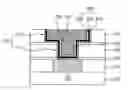
Referring to FIG. 1, an interlayer dielectric 110 and a lower metal line 120 made of an aluminum layer are formed on a semiconductor substrate 100. A passivation layer 130 is formed on the interlayer dielectric 110 to prevent the lower metal line 120 from being damaged in a subsequent etching process. The passivation layer 130 is made of a nitride-based layer.
A first insulation layer 140 and an etch barrier 150 for preventing the first insulation layer 140 from being etched in a subsequent process for etching a second insulation layer 160 are sequentially formed on the passivation layer 130. The second insulation layer 160 is then formed on the etch barrier 150. Each of the first and second insulation layers 140 and 160 is made of an oxide-based layer, and the etch barrier 150 is made of a nitride-based layer.
By etching the second insulation layer 160, the etch barrier 150, the first insulation layer 140, and the passivation layer 130, a via hole 171 is defined to expose the lower metal line 120. By additionally etching the second insulation layer 160 over the via hole 171 using the etch barrier 150 as an etch stop layer until the etch barrier 150 is exposed, a trench 172 is formed to delimit (or define) a metal line forming region. In this way, a dual type damascene pattern 170 comprised of the via hole 171 and the trench 172 is formed. Here, while the dual type damascene pattern 170 is formed by defining the trench 172 after defining the via hole 171, the sequence of forming the dual type damascene pattern 170 can be reversed.
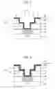
Referring to FIG. 2, a first WNx layer 210 is deposited on the second insulation layer 160 including the damascene pattern 170 comprised of the via hole 171 and the trench 172 to a thickness of 10˜200 Å. The first WNx layer 210 is formed through a chemical vapor deposition (CVD) or atomic layer deposition (ALD) process. The composition ratio x in the first WNx layer 210 is in the range of 0.1˜10.
Referring to FIG. 3, by surface-treating the first WNx layer 210, a WCyNx layer 220 is formed on the surface of the first WNx layer 210 to a thickness of 5˜50 Å. The surface treatment of the first WNx layer 210 is implemented through an heat treatment or plasma treatment under high temperature using a hydrocarbon-based gas such as CH3 or C2H5 gas containing “C—H—”. In the case where the surface treatment of the first WNx layer 210 is implemented through a plasma treatment, the plasma treatment is conducted under an atmosphere of CH3 or C2H5 at a temperature of 200˜500° C., a pressure of 1˜100 torr, and an RF power of 0.1˜1 kW.
Referring to FIG. 4, a second WNx layer 230 is deposited on the WCyNx layer 220 (which was formed through a surface treatment of the first WNx layer 210) to a thickness of 10˜200 Å. In this way, a diffusion barrier 240 made of a stack of the first WNx layer 210, the WCyNx layer 220, and the second WNx layer 230 is formed. The second WNx layer 230 is formed through a CVD or ALD process to improve the adhesion characteristics between a copper layer (to be subsequently formed) and the diffusion barrier 240.
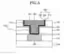
Referring to FIG. 5, a copper layer is deposited on the second WNx layer 230 to fill the trench 172 including the via hole 171 in which the diffusion barrier 240 made of the stack of the first WNx layer 210, the WCyNx layer 220, and the second WNx layer 230 is formed. Then, by performing a chemical mechanical polishing process (“CMPing”) on the copper layer until the second insulation layer 160 is exposed, a via contact 250 is formed in the via hole 171, and an upper metal line 260 made of copper is formed in the trench 172.
As is apparent from the above description, because the diffusion barrier of the present invention for preventing the diffusion of a copper metal line is formed in a stack structure of a first WNx layer, a WCyNx layer formed through surface treatment of the first WNx layer, and a second WNx layer, it is possible to form a diffusion barrier having superior diffusion prevention characteristics. As a consequence, it is possible to form a metal line having an excellent diffusion barrier in an ultra-highly integrated semiconductor device.
As a result, in the present invention, a metal line having an excellent diffusion barrier for copper can be formed in an ultra-highly integrated semiconductor device, whereby the characteristics of the semiconductor device can be improved.
In the above embodiment, a multi-layered metal line was illustrated and explained, which is formed through a dual damascene process wherein a copper layer is deposited in the first insulation layer 140 and the second insulation layer 160 having the dual type damascene pattern 170 including the via hole 171 and the trench 172 and the copper layer is then CMPed to form the via contact 240 in the via hole 171 and the upper metal line 250 in the trench 172. However, it is to be noted that the present invention is not limited to this exemplary embodiment such that the present invention can be applied to a multi-layered metal line which is formed through a single damascene process wherein a copper layer is deposited in an insulation layer having a trench for delimiting (or defining) a metal line forming region and the copper layer is then CMPed to form an upper metal line in the trench.
Although specific embodiments of the present invention have been described for illustrative purposes, those skilled in the art will appreciate that various modifications, additions and substitutions are possible, without departing from the scope and the spirit of the invention as disclosed in the accompanying claims.
Claims
What is claimed is:1. A multi-layered metal line of a semiconductor device comprising:
a lower metal line;
an upper metal line; and
a diffusion barrier formed between the lower and upper metal lines, wherein the diffusion barrier comprises a stack of a first WNx layer, a WCyNx layer, and a second WNx layer.
2. The multi-layered metal line according to claim 1, wherein the first WNx layer has a thickness of 10˜200 Å.
3. The multi-layered metal line according to claim 1, wherein the composition ratio x in the first WNx layer is in the range of 0.1˜10.
4. The multi-layered metal line according to claim 1, wherein the WCyNx layer has a thickness of 5˜50 Å.
5. The multi-layered metal line according to claim 1, wherein the second WNx layer has a thickness of 10˜200 Å.
6. A method for forming a diffusion barrier layer to prevent diffusion of a metal line in a semiconductor device formed with a multi-layered metal line structure, the method for forming a diffusion barrier comprising the steps of:
depositing a first WNx layer;
surface-treating the first WNx layer; and
depositing a second WNx layer on the surface-treated first WNx layer.
7. The method according to claim 6, wherein the first WNx layer is formed in a CVD or ALD process.
8. The method according to claim 6, wherein the first WNx layer is formed to a thickness of 10-200 Å.
9. The method according to claim 6, wherein the composition ratio x in the first WNx layer is 0.1˜10.
10. The method according to claim 6, wherein the step of surface-treating the first WNx layer comprises the step of:
forming a WCyNx layer on a surface of the first WNx layer through an heat treatment or plasma treatment under high temperature using a hydrocarbon-based source gas.
11. The method according to claim 10, wherein the hydrocarbon-based gas is CH3 or C2H5 gas.
12. The method according to claim 10, wherein the plasma treatment is implemented under an atmosphere of CH3 or C2H5 at a temperature of 200˜500 ° C., a pressure of 1˜100 torr, and an RF power of 0.1˜1 kW.
13. The method according to claim 10, wherein the WCyNx layer is formed to a thickness of 5˜50 Å.
14. The method according to claim 6, wherein the second WNx layer is formed in a CVD or ALD process.
15. The method according to claim 6, wherein the second WNx layer is formed to a thickness of 10˜200 Å.
16. A method for forming a multi-layered metal line of a semiconductor device, comprising the steps of:
forming an interlayer dielectric layer on a semiconductor substrate, the interlayer dielectric layer having a damascene pattern for defining a metal line forming region;
depositing a first WNx layer on the interlayer dielectric layer including the damascene pattern;
surface-treating the first WNx layer;
depositing a second WNx layer on the surface-treated first WNx layer so as to form a diffusion barrier comprising the surface-treated first WNx layer and the second WNx layer; and
forming a wiring metal layer on the diffusion barrier to fill the damascene pattern.
17. The method according to claim 16, wherein the damascene pattern is a single type or a dual type.
18. The method according to claim 17, wherein the single type damascene pattern has a trench.
19. The method according to claim 17, wherein the dual type damascene pattern has a via hole and a trench.
20. The method according to claim 16, wherein the first WNx layer is formed in a CVD or ALD process.
21. The method according to claim 16, wherein the first WNx layer is formed to a thickness of 10˜200 Å.
22. The method according to claim 16, wherein the composition ratio x in the first WNx layer is 0.1˜10.
23. The method according to claim 16, wherein the step of surface-treating the first WNx layer comprises the step of:
forming a WCyNx layer on a surface of the first WNx layer through an heat treatment or plasma treatment under high temperature using a hydrocarbon-based source gas.
24. The method according to claim 23, wherein the hydrocarbon-based gas is CH3 or C2H5 gas.
25. The method according to claim 23, wherein the plasma treatment is implemented under an atmosphere of CH3 or C2H5 at a temperature of 200˜500° C., a pressure of 1˜100 torr, and an RF power of 0.1˜1 kW.
26. The method according to claim 23, wherein the WCyNx layer is formed to a thickness of 5˜50 Å.
27. The method according to claim 16, wherein the second WNx layer is formed in a CVD or ALD process.
28. The method according to claim 16, wherein the second WNx layer is formed to a thickness of 10˜200 Å.
29. The method according to claim 16, wherein the wiring metal layer is made of a copper layer.
Images & Drawings included:
Sources:
- United States Patent and Trademark Office - verify current appl. status at the USPTO↗
Recent applications in this class:
- » 20250285918 2025-09-11
METHODS OF DEPOSITING IRIDIUM-CONTAINING FILMS FOR SEMICONDUCTOR DEVICES - » 20250218867 2025-07-03
SELECTIVE DEPOSITION OF CAPPING LAYER - » 20250112090 2025-04-03
Method Of Forming A Metal Liner For Interconnect Structures - » 20250079238 2025-03-06
METHOD OF FABRICATING A SEMICONDUCTOR DEVICE - » 20250029873 2025-01-23
METHOD FOR FABRICATING SEMICONDUCTOR DEVICE WITH LINER STRUCTURE - » 20250006552 2025-01-02
BOTTOM-UP GAP FILL PROCESSES FOR SEMICONDUCTOR SUBSTRATES - » 20240420997 2024-12-19
SELECTIVE LINER DEPOSITION FOR VIA RESISTANCE REDUCTION - » 20240395612 2024-11-28
CARBON-BASED LINER TO REDUCE CONTACT RESISTANCE - » 20240387259 2024-11-21
CONDUCTIVE STRUCTURES WITH BARRIERS AND LINERS OF VARYING THICKNESSES - » 20240387258 2024-11-21
FILM STACK SIMPLIFICATION FOR HIGH ASPECT RATIO PATTERNING AND VERTICAL SCALING
Recent applications for this Assignee:
- » 20130181761 2013-07-18
Trimming of operative parameters in electronic devices based on corrections mappings - » 20130087919 2013-04-11
LIGHTWEIGHT AND COMPACT THROUGH-SILICON VIA STACK PACKAGE WITH EXCELLENT ELECTRICAL CONNECTIONS AND METHOD FOR MANUFACTURING THE SAME - » 20130027076 2013-01-31
APPARATUS FOR DETECTING PATTERN ALIGNMENT ERROR - » 20120322216 2012-12-20
METHOD FOR REDUCING POLY-DEPLETION IN DUAL GATE CMOS FABRICATION PROCESS - » 20120231635 2012-09-13
Template derivative for forming ultra-low dielectric layer and method of forming ultra-low dielectric layer using the same - » 20120231634 2012-09-13
Template derivative for forming ultra-low dielectric layer and method of forming ultra-low dielectric layer using the same - » 20120217637 2012-08-30
Semiconductor package having substrate for high speed semiconductor package - » 20120205802 2012-08-16
PRINTED CIRCUIT BOARD AND FLIP CHIP PACKAGE USING THE SAME WITH IMPROVED BUMP JOINT RELIABILITY - » 20120115278 2012-05-10
STACKED SEMICONDUCTOR PACKAGE WITHOUT REDUCTION IN DATA STORAGE CAPACITY AND METHOD FOR MANUFACTURING THE SAME - » 20120088336 2012-04-12
SEMICONDUCTOR PACKAGE HAVING AN IMPROVED CONNECTION STRUCTURE AND METHOD FOR MANUFACTURING THE SAME