METHOD FOR PROCESSING WAFER IN REACTION CHAMBER
US20080169269A1
2008-07-17
11/744,459
2007-05-04
Abstract:
A method for processing a wafer in a reaction chamber is provided. The method includes the following steps: performing an over-etching, so as to have a sufficient oxide-layer isolation depth between metal wires; applying high-bias, high-watt plasma, so as to remove a reaction polymer on a surface of the wafer, and to remove the reaction polymer on the surface of the reaction chamber; and performing a static-eliminating procedure, so as to remove the static charges on the wafer, and then delivering the wafer out of the reaction chamber. Through the method with the high-bias, high-watt plasma of the present invention, the following efficacies can be achieved: (1) eliminating blemishes on the produced wafer; (2) prolonging a corrosion time of an aluminum-copper wire on the surface of the wafer; (3) prolonging an average cycle period for cleaning the reaction chamber; (4) shortening the time in the next acid tank; and (5) enhancing the yield of each wafer by 2-5%.
Assignee:
- LAM RESEARCH CO., LTD 1 🇹🇼 Hsinchu, Taiwan
Interested in similar patents?
Get notified when new applications in this technology area are published.
Classification:
H01L21/02071 » CPC main
Processes or apparatus adapted for the manufacture or treatment of semiconductor or solid state devices or of parts thereof; Manufacture or treatment of semiconductor devices or of parts thereof; Cleaning; Cleaning during device manufacture during, before or after processing of conductive layers, e.g. polysilicon or amorphous silicon layers the processing being a delineation, e.g. RIE, of conductive layers
H01L21/306 IPC
Processes or apparatus adapted for the manufacture or treatment of semiconductor or solid state devices or of parts thereof; Manufacture or treatment of semiconductor devices or of parts thereof the devices having at least one potential-jump barrier or surface barrier, e.g. PN junction, depletion layer or carrier concentration layer the devices having semiconductor bodies comprising elements of Group IV of the Periodic System or AB compounds with or without impurities, e.g. doping materials; Treatment of semiconductor bodies using processes or apparatus not provided for in groups - to change their surface-physical characteristics or shape, e.g. etching, polishing, cutting Chemical or electrical treatment, e.g. electrolytic etching
Description
FIELD OF THE INVENTION
The present invention relates to a method for processing a wafer. More particularly, the present invention relates to a method for processing a wafer with a step of applying high-bias, high-watt plasma in a reaction chamber, so as to remove a reaction polymer on a surface of a wafer and to remove the reaction polymer on the surface of the reaction chamber.
DESCRIPTION OF THE PRIOR ART
The common process for fabricating a wafer does not remove a reaction polymer on the surface of the wafer by utilizing high-bias, high-watt plasma, but only carries away a small amount of the reaction polymer from the surface of the wafer by using a gas flow and a low pressure, which results in a poor effect.
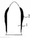
During the conventional process for fabricating a wafer 1, as shown in FIG. 1, a reaction polymer 2 generated after etching the wafer 1 will be attached to the surface of the wafer 1, which easily causes the following defects:
1. if it takes a long time to react in the acid tank, the acid solution should be changed frequently, or the acid tank is often contaminated by the reaction polymer;
2. the chlorine-containing reaction polymer 2 on the surface of the wafer 1 is likely to corrode the aluminum wire on the surface on the wafer 1, which causes a disconnection of the aluminum wire or an increment in the impedance and capacitance. As a result, the wafer 1 is discarded, or the yield and the reliability of the wafer 1 are severely affected;
3. the reaction polymer 2, which is attached to both sides of the aluminum wire and forms a thick rabbit ear, cannot be easily removed in the acid tank, which causes difficulties in the subsequent step of filling oxide, and thus the rabbit ear is not allowed to exist; and
4. a large amount of micro reaction polymer 2 has accumulated around the edge of the wafer 1, so that the micro reaction polymer 2 flows back to the surface of the wafer 1 upon being etched, which results in a low yield.
SUMMARY OF INVENTION
In the present invention, a step of applying high-bias, high-watt plasma is added between the over-etching step and the static-eliminating step during a conventional process for fabricating a wafer 1, so that the reaction polymer 2 on the wafer 1 can be effectively removed, without affecting the original specification of the wafer 1.
The present invention relates to a method for processing a wafer 1 in a reaction chamber. The method includes the following steps: performing an over-etching, so as to have a sufficient oxide layer isolation depth between metal wires; applying high-bias, high-watt plasma, so as to remove a reaction polymer 2 on the surface of the wafer 1, and to remove the reaction polymer 2 on the surface of the reaction chamber; and performing a static-eliminating procedure, so as to eliminate the static charges on the wafer 1, and then, delivering the wafer out of the reaction chamber.
BRIEF DESCRIPTION OF THE DRAWINGS
FIG. 1 shows a reaction polymer attached to a surface of a wafer during a conventional process for fabricating the wafer;
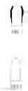
FIG. 2 shows that the reaction polymer is no longer attached to the surface of the wafer after the step of applying high-bias, high-watt plasma of the present invention; and
FIG. 3 is a flow chart for implementing the present invention.
DETAILED DESCRIPTION
In the present invention, a step of applying high-bias, high-watt plasma is added between the over-etching step and the static-eliminating step during a conventional process for fabricating a wafer 1. As shown in FIG. 2, through the method of the present invention, a reaction polymer 2 on the wafer 1 can be effectively removed, without affecting the original specification of the wafer 1.
FIG. 3 is a flow chart for implementing the present invention, which includes the following steps: performing an over-etching (Step 10), so as to have a sufficient isolation depth of an oxide layer between metal wires; applying high-bias, high-watt plasma (Step 20), so as to remove a reaction polymer 2 on the surface of the wafer 1, and to remove the reaction polymer 2 on the surface of a reaction chamber; and performing a static-eliminating step (Step 30), so as to eliminate the static charges on the wafer 1, and then, delivering the wafer out of the reaction chamber. In Step 20, the time for applying the plasma falls in a range from 5 to 60 seconds, in which the plasma includes boron trichloride (BCl3) and an argon gas (Ar); the pressure of the plasma falls in a range from 6 to 12 mTorr; the upper power and the lower power of the plasma fall in a range from 300 to 1200 watts and in a range from 250 to 900 watts respectively; and the flow rates of BCl3 and Ar contained in the plasma fall in a range from 10 to 200 sccm and in a range from 100 to 1000 sccm respectively. Additionally, BCl3 contained in the plasma can be replaced by a nitrogen gas or an oxygen gas, and the flow of the nitrogen gas or the oxygen gas falls in a range from 10 to 200 sccm.
Through the method of the present invention, the following effects can be achieved.
1. A reaction polymer 2 close to the surface of a reaction chamber of a wafer 1 can be removed with high-bias, high-watt plasma of the present invention, so as to prevent the reaction polymer 2 from returning to the surface of the wafer 1 to hamper etching or cause partial etching, and thus, blemishes during the process for fabricating the wafer 1 can be reduced, and the yield of the wafer can be improved;
2. The “rabbit ear” on each side of an aluminum wire and the reaction polymer 2 can be effectively removed by the high-bias plasma of the present invention, and the corrosion-resistant time for an aluminum-copper wire on the surface of the wafer 1 can be greatly prolonged over 96 hours, in the absence of the reaction polymer 2;
3. the reaction polymer 2 on the surface of the reaction chamber can also be removed after the step of applying the high-bias, high-watt plasma of the present invention, so that the average cycle period for cleaning the reaction chamber is prolonged;
4. the reaction polymer 2 on the surface of the wafer 1 has almost been removed, so that the time in the next acid tank is greatly reduced; and
5. the yield of each wafer can be enhanced by 2-5%.
Claims
What is claimed is:1. A method for processing a wafer in a reaction chamber, comprising the following steps:
performing an over-etching step, to have a sufficient oxide-layer isolation depth between metal wires;
applying high-bias, high-watt plasma, to remove a reaction polymer on a surface of the wafer, and to remove the reaction polymer on the surface of the reaction chamber; and
performing a static charge-eliminating step, to eliminate static charges on the wafer, and then, to deliver the wafer out of the reaction chamber.
2. The method as claimed in claim 1, wherein the pressure of the plasma falls in a range from 6 to 12 mTorr.
3. The method as claimed in claim 1, wherein the upper power of the plasma falls in a range from 300 to 1200 watts.
4. The method as claimed in claim 1, wherein the lower power of the plasma falls in a range from 250 to 900 watts.
5. The method as claimed in claim 1, wherein the plasma comprises a boron trichloride and an argon gas.
6. The method as claimed in claim 5, wherein boron trichloride is replaced by a nitrogen gas or an oxygen gas.
7. The method as claimed in claim 1, wherein the time for applying the plasma falls in a range from 5 to 60 seconds.
8. The method as claimed in claim 5, wherein the flow rate of the boron trichloride falls in a range from 10 to 200 sccm.
9. The method as claimed in claim 6, wherein the flow rate of the nitrogen gas or the oxygen gas falls in a range from 10 to 200 sccm.
10. The method as claimed in claim 5, wherein the flow rate of the argon gas falls in a range from 100 to 1000 sccm.
Images & Drawings included:

Sources:
- United States Patent and Trademark Office - verify current appl. status at the USPTO↗
Recent applications in this class:
- » 20230055179 2023-02-23
PREPARATION METHOD OF METAL CONNECTING LINE - » 20210320002 2021-10-14
WATER SOLUBLE POLYMERS FOR PATTERN COLLAPSE MITIGATION - » 20190259600 2019-08-22
Mechanisms for forming patterns using multiple lithography processes - » 20190088470 2019-03-21
Fill material to mitigate pattern collapse - » 20180315594 2018-11-01
Method of cleaning and drying semiconductor substrate - » 20180166272 2018-06-14
Enhanced charged particle beam processes for carbon removal - » 20180138033 2018-05-17
Removal of metal - » 20180033611 2018-02-01
Cluster tool and manufacuturing method of semiconductor structure using the same - » 20170372891 2017-12-28
Mechanisms for forming patterns using multiple lithography processes - » 20170178895 2017-06-22
Method for cleaning substrate