METHOD FOR DESIGNING A LEADLESS CHIP CARRIER
US20080187722A1
2008-08-07
11/672,258
2007-02-07
Abstract:
A method for surface mounting a leadless chip carrier to a circuit board, the method includes the steps of providing the leadless chip carrier with chamfered edges along one or more sides and with package metallic connection portions disposed along one or more chamfered edges; providing the circuit board with a plurality of circuit board metallic connection portions; placing a layer of solder onto the circuit board metallic connection; placing the leadless chip carrier on the circuit board with the package metallic connections, layer of solder and the circuit board metallic connections aligned; and heating the leadless chip carrier and the circuit board so the layer of solder forms a solder joint with the package metallic connection portions and the circuit board metallic connections.
Interested in similar patents?
Get notified when new applications in this technology area are published.
Classification:
H05K3/3442 » CPC main
Apparatus or processes for manufacturing printed circuits; Assembling printed circuits with electric components, e.g. with resistor electrically connecting electric components or wires to printed circuits by soldering; Surface mounted components; Leadless components having edge contacts, e.g. leadless chip capacitors, chip carriers
H01L23/13 » CPC further
Details of semiconductor or other solid state devices; Mountings, e.g. non-detachable insulating substrates characterised by the shape
H01L23/49805 » CPC further
Details of semiconductor or other solid state devices; Arrangements for conducting electric current to or from the solid state body in operation, e.g. leads, terminal arrangements ; Selection of materials therefor consisting of soldered constructions; Leads, on insulating substrates, the leads being also applied on the sidewalls or the bottom of the substrate, e.g. leadless packages for surface mounting
H01L27/14618 » CPC further
Devices consisting of a plurality of semiconductor or other solid-state components formed in or on a common substrate including semiconductor components sensitive to infra-red radiation, light, electromagnetic radiation of shorter wavelength or corpuscular radiation and specially adapted either for the conversion of the energy of such radiation into electrical energy or for the control of electrical energy by such radiation; Devices controlled by radiation; Imager structures; Structural or functional details thereof Containers
H01L27/14683 » CPC further
Devices consisting of a plurality of semiconductor or other solid-state components formed in or on a common substrate including semiconductor components sensitive to infra-red radiation, light, electromagnetic radiation of shorter wavelength or corpuscular radiation and specially adapted either for the conversion of the energy of such radiation into electrical energy or for the control of electrical energy by such radiation; Devices controlled by radiation; Imager structures Processes or apparatus peculiar to the manufacture or treatment of these devices or parts thereof
H05K2201/09154 » CPC further
Indexing scheme relating to printed circuits covered by; Shape and layout; Edge details Bevelled, chamferred or tapered edge
H05K2201/09154 » CPC further
Indexing scheme relating to printed circuits covered by; Shape and layout; Edge details Bevelled, chamferred or tapered edge
H05K2201/10727 » CPC further
Indexing scheme relating to printed circuits covered by; Details of components or other objects attached to or integrated in a printed circuit board; Details of electrical connections of non-printed components, e.g. special leads; Components characterised by their electrical contacts Leadless chip carrier [LCC], e.g. chip-modules for cards
Y02P70/50 » CPC further
Climate change mitigation technologies in the production process for final industrial or consumer products Manufacturing or production processes characterised by the final manufactured product
Y02P70/50 » CPC further
Climate change mitigation technologies in the production process for final industrial or consumer products Manufacturing or production processes characterised by the final manufactured product
Y10T428/24777 » CPC further
Stock material or miscellaneous articles; Structurally defined web or sheet [e.g., overall dimension, etc.] Edge feature
H01L2924/0002 » CPC further
Indexing scheme for arrangements or methods for connecting or disconnecting semiconductor or solid-state bodies as covered by; Technical content checked by a classifier Not covered by any one of groups , and
H01L2924/00 » CPC further
Indexing scheme for arrangements or methods for connecting or disconnecting semiconductor or solid-state bodies as covered by
B32B33/00 IPC
Layered products characterised by particular properties or particular surface features, e.g. particular surface coatings; Layered products designed for particular purposes not covered by another single class
B23K31/02 IPC
Processes relevant to this subclass, specially adapted for particular articles or purposes, but not covered by only one of the preceding main groups relating to soldering or welding
Description
FIELD OF THE INVENTION
The invention relates generally to the field of image sensor packaging, and more particularly, to providing chamfered edges on the image sensor package to enhance mounting of the package to a circuit board.
BACKGROUND OF THE INVENTION
Referring to FIGS. 1 and 2, currently, image sensors 10 include a plurality of pixels 20 housed in a rectangular enclosure 30, commonly referred to as a ceramic package, having sides 40 that extend perpendicular from the top of the enclosure 30. Metal contacts 50 extend downwardly along the sides of the enclosure. Referring to FIG. 3, the image sensor is placed on a circuit board 60 by soldering 70 and the like.
Although the current method is satisfactory, improvements in the packaging method are always desirable.
SUMMARY OF THE INVENTION
The present invention is directed to overcoming one or more of the problems set forth above. Briefly summarized, according to one aspect of the present invention, the present invention resides in a method for surface mounting a leadless chip carrier to a circuit board, the method comprising the steps of providing the leadless chip carrier with chamfered edges along one or more sides and with package metallic connection portions disposed along one or more chamfered edges; providing the circuit board with a plurality of circuit board metallic connection portions; placing a layer of solder onto the circuit board metallic connection; placing the leadless chip carrier on the circuit board with the package metallic connections, layer of solder and the circuit board metallic connections aligned; and heating the leadless chip carrier and the circuit board so the layer of solder forms a solder joint with the package metallic connection portions and the circuit board metallic connections.
These and other aspects, objects, features and advantages of the present invention will be more clearly understood and appreciated from a review of the following detailed description of the preferred embodiments and appended claims, and by reference to the accompanying drawings.
ADVANTAGEOUS EFFECT OF THE INVENTION
The present invention has the following advantages of reduced stress points acting on the solder joint during temperature cycling of the package that is soldered to a circuit board. This reduced stress will reduce the creation of solder cracking.
The coefficient of thermal expansion (CTE) of the ceramic package, preferably alumina (Al2O3), is approximately 7 ppm per degree C. and typical circuit board material is 1.5× to over 2× the coefficient of thermal expansion. The soldering process firmly attaches the electronic package to the circuit board creating an assembly. When the assembly is heated or cooled, the variation in CTE causes stress to be created at the solder joints. Cycling the assembly from cold (−40 C) to hot (+85) can fatigue the solder joints and induce stress cracks in the solder. The stress cracks create open circuit, which render the circuit board defective. The no lead solders are more brittle than leaded versions and hence they will have a higher propensity to crack.
The prior art ceramic surface mount packages have a sharp edge. This edge is a stress concentration point that will be a crack generation point. In contrast, the chamfered edge of the present invention allows for a reduced stress concentration area over the sharp edge of the prior art ceramic surface mount package. Modeling has shown that this reduction in stress concentration will allow the solder to survive thermal cycling beyond what can be achieved with the current sharp edges. The modeling data reveals at least a 6× improvement can be obtained.
BRIEF DESCRIPTION OF THE DRAWINGS
FIG. 1 is a top view of a prior art image sensor and its associated ceramic package;
FIG. 2 is a side view of FIG. 1;
FIG. 3 is a cross sectional view of FIG. 1;
FIG. 4 is a top view of the image sensor of the present invention;
FIG. 5 is a side view of FIG. 4;
FIG. 6 is a cross sectional view of FIG. 4; and
FIG. 7 is a top view of the circuit board of the present invention.
DETAILED DESCRIPTION OF THE INVENTION
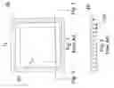
Referring to FIG. 4, there is shown a top view of the leadless, ceramic chip carrier 80 of the present invention. The carrier includes a plurality of pixels 90 arranged in a two dimensional array for collecting charge, preferably electrons, in response to light. The pixels 90 are packaged in the leadless, ceramic chip carrier 80 which surrounds the pixels 90. Referring to FIG. 5, a plurality of metallic contacts 100 are disposed along one or more sides 110, typically all four sides, that form electrical connections between the leadless, ceramic chip carrier 80 and a circuit board 120 (see FIG. 7) which will be attached thereto. Although the sides 110 shown a straight edge, the sides 110 could have castellations. All four sides preferably include a chamfered edge 130 which facilitates efficient attachment to the circuit board 120, as will be described hereinbelow. The chamfered edge 130 is preferably forty-five degrees or substantially between thirty degrees and sixty degrees.
Referring to FIG. 6, there is shown the leadless, ceramic chip carrier 80 attached to the circuit board 120. The circuit board 120 includes a two-dimensional substrate having a plurality of metallic contacts 140 (see FIG. 7) that spatially align with the metallic contacts 100 of the leadless, ceramic chip carrier 80.
Referring to FIG. 6, the leadless, ceramic chip carrier 80 is attached by either of two methods. The first method includes placing a layer of solder 150 on the metallic contacts 140 (see FIG. 7) of the circuit board 120. The leadless, ceramic chip carrier 80 is positioned on the circuit board 120 so that the metallic contacts 100 of the leadless, ceramic chip carrier 80, solder 150 and metallic contacts 140 of the circuit board are aligned in a one-to-one relationship. This entire assembly is heated so that the solder 150 melts and eventually spreads out to form a joint for the chip carrier 80 along its chamfered edges 130 and the circuit board 120. The second method preferably includes the circuit board 120 and the chip carrier 80 having their respective metal contacts 100 and 140 aligned. The chip carrier 80 is then placed atop the circuit board 120 with the metallic connections 100 and 140 spatially aligned in a one-to-one relationship. The interface formed by the metallic contacts 100 and 140 have molten solder applied which causes a soldered joint along the chamfered edges 130 and the circuit board 120.
The invention has been described with reference to a preferred embodiment. However, it will be appreciated that variations and modifications can be effected by a person of ordinary skill in the art without departing from the scope of the invention.
PARTS LIST
- 10 prior art image sensor
- 20 pixels
- 30 prior art image sensor package
- 40 sides of package
- 50 package metal contacts
- 60 circuit board
- 70 solder
- 80 leadless, ceramic chip carrier
- 90 pixels
- 100 metallic contacts on package
- 110 sides of package
- 120 circuit board
- 130 chamfered edges
- 140 circuit board metallic contacts
- 150 solder
Claims
1. A method for surface mounting a leadless chip carrier to a circuit board, the method comprising the steps of:
(a) providing the leadless chip carrier with chamfered edges along one or more sides and with package metallic connection portions disposed along one or more chamfered edges;
(b) providing the circuit board with a plurality of circuit board metallic connection portions;
(c) placing a layer of solder onto the circuit board metallic connection;
(d) placing the leadless chip carrier on the circuit board with the package metallic connections, layer of solder and the circuit board metallic connections aligned; and
(e) heating the leadless chip carrier and the circuit board so the layer of solder forms a solder joint with the package metallic connection portions and the circuit board metallic connections.
2. The method as in claim 1, wherein step (a) includes providing a leadless chip carrier packaged image sensor as the leadless chip carrier.
3. The method as in claim 2, wherein step (a) includes providing substantially forty-five degree angles forming the chamfered edges.
4. The method as in claim 2, wherein step (a) includes providing a range of substantially between angles of thirty degrees and sixty degrees for forming the chamfered edges.
5. A surface mount assembly comprising:
(a) a leadless chip carrier with chamfered edges along one or more sides and with metallic connection portions disposed along one or more chamfered edges; and
(b) a circuit board with a plurality of solder pads; wherein the leadless chip carrier and the circuit board have solder joints at an aligned connection of the solder pads to the metallic connection portions of the leadless chip carrier.
6. The surface mount assembly as in claim 5, wherein the leadless chip carrier is a leadless chip carrier packaged image sensor.
7. The surface mount assembly as in claim 6, wherein the chamfered edges are substantially forty-five degree angles.
8. The surface mount assembly as in claim 6, wherein the chamfered edges are substantially between a range of thirty degrees and sixty degrees.
9. A method for surface mounting a leadless chip carrier to a circuit board, the method comprising the steps of:
(a) providing the leadless chip carrier with chamfered edges along one or more sides and with package metallic connection portions disposed along one or more chamfered edges;
(b) providing the circuit board with a plurality of circuit board metallic connection portions;
(c) placing the leadless chip carrier on the circuit board with the package metallic connections and the circuit board metallic connections aligned for forming an interface; and
(d) applying solder to the interface.
10. The method as in claim 9, wherein step (a) includes providing a leadless chip carrier packaged image sensor as the leadless chip carrier.
11. The method as in claim 10, wherein step (a) includes providing substantially forty-five degree angles forming the chamfered edges.
12. The method as in claim 10, wherein step (a) includes providing a range of substantially between angles of thirty degrees and sixty degrees for forming the chamfered edges.
Images & Drawings included:


Sources:
- United States Patent and Trademark Office - verify current appl. status at the USPTO↗
Recent applications in this class:
- » 20240268036 2024-08-08
METHOD FOR PRODUCING ELECTRONIC COMPONENT MOUNTED SUBSTRATE - » 20190387630 2019-12-19
Electronic component with flexible terminal - » 20190254173 2019-08-15
Circuit board assembly inspection method - » 20190075660 2019-03-07
Electronic device and method of manufacturing the same - » 20190059161 2019-02-21
Compact printed circuit board assembly with insulating endcap via - » 20180359864 2018-12-13
METAL ELECTRODE LEADLESS FACE (MELF) DEVICE CRADLE - » 20180116055 2018-04-26
Electronic-component mount substrate, electronic device, and electronic module - » 20180042122 2018-02-08
Electronic component - » 20170359906 2017-12-14
Electronic device - » 20150230345 2015-08-13
Interdigitated chip capacitor assembly