N-type carbon nanotube field effect transistor and method of fabricating the same
US20080191280A1
2008-08-14
12/107,318
2008-04-22
✅ Patent granted
US 7,705,347 B2
2010-04-27
-
-
Douglas M Menz
2028-10-17
Abstract:
Provided are an n-type carbon nanotube field effect transistor (CNT FET) and a method of fabricating the n-type CNT FET. The n-type CNT FET may include a substrate; electrodes formed on the substrate and separated from each other; a CNT formed on the substrate and electrically connected to the electrodes; a gate oxide layer formed on the CNT; and a gate electrode formed on the gate oxide layer, wherein the gate oxide layer contains electron donor atoms which donate electrons to the CNT such that the CNT may be n-doped by the electron donor atoms.
Inventors:
- Wan Jun PARK 49 🇰🇷 Seoul, South Korea
- Yo-sep Min 18 🇰🇷 Yongin-si, South Korea
- Eun-Ju Bae 10 🇰🇷 Yongin-si, South Korea
Assignee:
- SAMSUNG ELECTRONICS CO., LTD. 16,784 🇰🇷 Gyeonggi-Do, South Korea
- Samsung Electronics Co.,Ltd. 182 🇰🇷 Suwon-si, South Korea
Interested in similar patents?
Get notified when new applications in this technology area are published.
Classification:
H01L51/002 » CPC main
Solid state devices using organic materials as the active part, or using a combination of organic materials with other materials as the active part; Processes or apparatus specially adapted for the manufacture or treatment of such devices, or of parts thereof; Processes specially adapted for the manufacture or treatment of devices or of parts thereof Making n- or p-doped regions
B82Y10/00 » CPC further
Nanotechnology for information processing, storage or transmission, e.g. quantum computing or single electron logic
H01L51/0525 » CPC further
Solid state devices using organic materials as the active part, or using a combination of organic materials with other materials as the active part; Processes or apparatus specially adapted for the manufacture or treatment of such devices, or of parts thereof specially adapted for rectifying, amplifying, oscillating or switching, or capacitors or resistors with at least one potential- jump barrier or surface barrier multistep processes for their manufacture the devices being controllable only by the electric current supplied or the electric potential applied, to an electrode which does not carry the current to be rectified, amplified or swiched, e.g. three-terminal devices; Field-effect devices, e.g. TFTs insulated gate field effect transistors characterised by the gate dielectric the gate dielectric comprising only inorganic materials
H01L51/0048 » CPC further
Solid state devices using organic materials as the active part, or using a combination of organic materials with other materials as the active part; Processes or apparatus specially adapted for the manufacture or treatment of such devices, or of parts thereof; Selection of organic semiconducting materials, e.g. organic light sensitive or organic light emitting materials; Carbon containing materials, e.g. carbon nanotubes, fullerenes Carbon nanotubes
H01L51/0541 » CPC further
Solid state devices using organic materials as the active part, or using a combination of organic materials with other materials as the active part; Processes or apparatus specially adapted for the manufacture or treatment of such devices, or of parts thereof specially adapted for rectifying, amplifying, oscillating or switching, or capacitors or resistors with at least one potential- jump barrier or surface barrier multistep processes for their manufacture the devices being controllable only by the electric current supplied or the electric potential applied, to an electrode which does not carry the current to be rectified, amplified or swiched, e.g. three-terminal devices; Field-effect devices, e.g. TFTs insulated gate field effect transistors Lateral single gate single channel transistors with non inverted structure, i.e. the organic semiconductor layer is formed before the gate electode
Y10S977/938 » CPC further
Nanotechnology; Specified use of nanostructure for electronic or optoelectronic application in a transistor or 3-terminal device Field effect transistors, FETS, with nanowire- or nanotube-channel region
H01L29/786 IPC
Semiconductor devices adapted for rectifying, amplifying, oscillating or switching, or capacitors or resistors with at least one potential-jump barrier or surface barrier, e.g. PN junction depletion layer or carrier concentration layer; Details of semiconductor bodies or of electrodes thereof; Multistep manufacturing processes therefor; Types of semiconductor device ; Multistep manufacturing processes therefor controllable by only the electric current supplied, or only the electric potential applied, to an electrode which does not carry the current to be rectified, amplified or switched; Unipolar devices, e.g. field effect transistors; Field effect transistors with field effect produced by an insulated gate Thin film transistors, i.e. transistors with a channel being at least partly a thin film
H01L35/24 IPC
Thermoelectric devices comprising a junction of dissimilar materials, i.e. exhibiting Seebeck or Peltier effect with or without other thermoelectric effects or thermomagnetic effects; Processes or apparatus peculiar to the manufacture or treatment thereof or of parts thereof; Details thereof; Selection of the material for the legs of the junction using organic compositions
Description
CROSS-REFERENCE TO RELATED APPLICATIONS
This application claims the benefit of Korean Patent Application No. 10-2004-0078544, filed on Oct. 2, 2004, in the Korean Intellectual Property Office, and as a divisional application of U.S. application Ser. No. 11/192,107, filed Jul. 29, 2005, the entire contents of which are incorporated herein by reference.
1. Field of the Disclosure
Embodiments of the present disclosure relate to a field effect transistor (FET) having n-doped carbon nanotube (CNT) and a method of fabricating the n-type CNT FET, and more particularly, to an n-type CNT FET having n-doped CNT which may be manufactured by adsorbing electron donor atoms on a CNT layer and a method of fabricating the n-type CNT FET.
2. Description of the Related Art
CNTs have excellent mechanical and chemical properties and may have a long length of up to one micrometer with a diameter ranging from several nanometers to several tens of nanometers. CNTs have excellent electrical conductivity and may be applied to electronic devices. Vigorous research has been conducted on the use of CNTs in various devices and they are now used in electric field emission devices, optical switches in the field of optical communication, biodevices, etc.
Methods of manufacturing CNTs are well known in the art. Examples include arc discharge, pulsed laser vaporization, chemical vapor deposition, screen printing and spin coating.
To use CNTs in a semiconductor device, such as a complementary metal-oxide-semiconductor (CMOS) transistor, p-type and n-type MOS transistors are required. In general, CNTs are easily to be hole-doped (p-type doped).
U.S. Patent Application Publication No. 2003-122,133 describes a method of manufacturing an n-type nanotube using an oxygen or potassium ion as a dopant. However, an oxygen molecule cannot be easily decomposed into oxygen atoms and it is difficult to handle potassium ions.
To overcome these problems, U.S. Pat. No. 6,723,624 suggests another n-type doping method. In this method, silicon nitride (SiNx) is deposited on the CNT using plasma-enhanced chemical vapor-phased deposition (PECVD), and then heated, thereby manufacturing an n-type (electron-doped) CNT.
SUMMARY OF THE DISCLOSURE
Embodiments of the present disclosure may provide a field effect transistor (FET) having n-doped CNT which may be manufactured by forming a gate oxide layer containing electron donor atoms on a CNT layer, which may be a channel region, and a method of fabricating the n-type CNT FET.
According to an aspect of the present disclosure, there may be provided an n-type CNT FET comprising: a substrate; electrodes formed on the substrate and separated from each other; a CNT formed on the substrate and electrically connected to the electrodes; a gate oxide layer formed on the CNT; and a gate electrode formed on the gate oxide layer, wherein the gate oxide layer may contain electron donor atoms which donate electrons to the CNT such that the CNT may be n-doped by the electron donor atoms.
The gate oxide layer may be formed by depositing an oxide or a nitride containing a group V atom using an atomic layer deposition (ALD) process.
The group V atom may be bismuth.
The oxide may be bismuth titanium silicon oxide (BTSO).
According to another aspect of the present disclosure, there may be provided an n-type CNT FET comprising: a conductive substrate; a gate oxide layer formed on the conductive substrate; electrodes formed on the gate oxide layer and separated from each other; and a CNT formed on the gate oxide layer and electrically connected to the electrodes; wherein the gate oxide layer contains electron donor atoms which donate electrons to the CNT such that the CNT may be n-doped by the electron donor atoms.
According to still another aspect of the present disclosure, there may be provided a method of fabricating an n-type CNT FET comprising: forming electrodes separated from each other on a substrate; forming a CNT on the substrate such that the CNT may be electrically connected to the electrodes; forming a gate oxide layer on the CNT by depositing an oxide or a nitride containing electron donor atoms; forming a gate electrode on the gate oxide layer, wherein the CNT may be n-doped by the electron donor atoms.
According to yet another aspect of the present invention, there may be provided a method of fabricating an n-type CNT FET, comprising: forming a gate oxide layer on a conductive substrate by depositing an oxide or a nitride containing electron donor atoms on the substrate; forming electrodes separated from each other on the gate oxide layer; and forming a CNT on the gate oxide layer such that the CNT may be electrically connected to the electrodes, wherein the CNT may be n-doped by the electron donor atoms.
BRIEF DESCRIPTION OF THE DRAWINGS
The above and other features and advantages of embodiments of the present invention will become more apparent by describing in detail exemplary embodiments thereof with reference to the attached drawings in which:
FIG. 1 is a cross-sectional view of an n-type carbon nanotube field effect transistor (CNT FET) according to an embodiment of the present invention;
FIG. 2 is a cross-sectional view of an n-type CNT FET according to another embodiment of the present invention;
FIGS. 3 and 4 are I-V graphs of CNT FETs before and after the deposition of bismuth titanium silicon oxide (BTSO);
FIGS. 5A through 5E are cross-sectional views illustrating a method of fabricating an n-type CNT FET according to an embodiment of the present invention; and
FIGS. 6A through 6C are cross-sectional views illustrating a method of fabricating an n-type CNT FET according to another embodiment of the present invention.
DETAILED DESCRIPTION OF EXEMPLARY EMBODIMENT OF THE DISCLOSURE
Hereinafter, an n-type carbon nanotube field effect transistor (CNT FET) having an n-type CNT and a method of fabricating the n-type CNT FET according to embodiments of the disclosure will be described in detail with reference to the attached drawings.
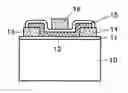
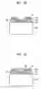
FIG. 1 is a cross-sectional view of an n-type CNT FET according to an embodiment of the disclosure.
Referring to FIG. 1, an insulating layer 11 may be formed on a substrate 10. A CNT 12 may be formed on the insulating layer 11 and electrodes 13 and 14 may be formed on both ends of the CNT 12, respectively. The electrodes 13 and 14 may function as a drain region and a source region, respectively, and the CNT 12 may function as a channel region.
A gate oxide layer 15 may cover the CNT 12 and a gate electrode 16 may be formed on the gate oxide layer 15, between the electrodes 13 and 14.
The gate oxide layer 15 may be formed of an oxide or a nitride and may function as an electron donor layer. The gate oxide layer 15 may contain a group V atom, such as N, P, As, Sb or Bi. The gate oxide layer 15 may be composed of bismuth titanium silicon oxide (BTSO) and may be formed using an atomic layer deposition (ALD) process. When the CNT 22 is deposited on the BTSO layer, the bismuth may donate electrons to the CNT 12, thereby n-doping a surface of the CNT 12. The electronic device illustrated in FIG. 1 is a top gate n-type CNT FET.
FIG. 2 is a cross-sectional view of an n-type CNT FET according to another embodiment of the present disclosure.
Referring to FIG. 2, a gate oxide layer 21 may be formed on a conductive substrate 20, for example, a highly doped silicon wafer. A CNT 22 may be formed on the gate oxide layer 21 and electrodes 23 and 24 may be formed below both ends of the CNT 22, respectively. The electrodes 23 and 24 may function as a drain region and a source region, respectively, and the CNT 22 may function as a channel region. The conductive substrate 20 functions as a gate electrode.
The gate oxide layer 21 may be formed of an oxide or a nitride and may function as an electron donor layer. The gate oxide layer 21 may contain a group V atom, such as N, P, As, Sb or Bi. The gate oxide layer 21 may be composed of BTSO and may be formed using an ALD process. When the BTSO layer is deposited on the CNT 22, the bismuth may donate electrons to the CNT 22, thereby n-doping a surface of the CNT 22. The electronic device illustrated in FIG. 2 is a bottom gate n-type CNT FET.
FIGS. 3 and 4 are I-V graphs of CNT FETs before and after the deposition of BTSO, respectively.
Referring to FIG. 3, CNT before deposition of BTSO may be slightly p-doped. When a voltage Vds is applied to a drain electrode and a source electrode and a gate bias voltage Vg is applied in the negative direction, the transistor may be turned on. Thus, the CNT may exhibit p-type characteristics.
Referring to FIG. 4, CNT after deposition of BTSO may be n-doped. When a voltage Vds is applied to a drain electrode and a source electrode and a gate bias voltage Vg is applied in the positive direction, the transistor may be turned on. Thus, the CNT exhibits n-type characteristics. Thus, the CNT is n-doped by depositing BSTO on the CNT.
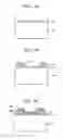
FIGS. 5A through 5E are cross-sectional views illustrating a method of fabricating an n-type CNT FET according to an embodiment of the present disclosure.
Referring to FIG. 5A, an insulating layer 31, for example, an oxide layer, may be formed on a substrate 30. When the substrate 30 is made of a non-conductive material, the insulating layer 31 may be omitted.
Referring to FIG. 5B, a conductive layer may be formed on the insulating layer 31 and patterned to form a drain electrode 33 and a source electrode 34, which are separated from each other.
Referring to FIG. 5C, a CNT 32 may be formed on the insulating layer 31 such that the CNT 32 is electrically connected to the electrodes 33 and 34. The CNT 32 may be grown directly on the insulating layer 31 or formed using a conventional method, such as screen printing, spin coating, etc. This CNT 32 may exhibit p-type characteristics.
Referring to FIG. 5D, a gate oxide layer 35 may be deposited on the CNT 32. The gate oxide layer 35 may be formed by depositing BTSO using an ALD process at 300° C. Water vapor may be used as an oxygen source. When the BTSO layer is deposited on the CNT 32, electrons from the BTSO layer may be adsorbed by a surface of the CNT 32, and thus, the CNT 32 may be n-doped. Since the gate oxide layer 35 may be used as an electron donor layer, the n-doping may be easily performed in a simplified process.
Although the gate oxide layer 35 may be formed of an oxide in the above description, the composition of the gate oxide layer 35 need not be limited thereto. The gate oxide layer 35 may contain one of N, P, As, Sb and Bi, which are group V atoms.
Referring to FIG. 5E, a gate electrode 36 may be formed on the gate oxide layer 35, between the electrodes 33 and 34. The gate electrode 36 may be formed using a pattering process.
FIGS. 6A through 6C are cross-sectional views illustrating a method of fabricating an n-type CNT FET according to another embodiment of the disclosure.
Referring to FIG. 6A, a gate oxide layer 41 may be formed on a conductive substrate 40, such as a highly doped silicon substrate. The gate oxide layer 41 may be formed by depositing BTSO using an ALD process at about 3000C. Water vapor may be used as an oxygen source.
Referring to FIG. 6B, a conductive layer may be formed on the gate oxide layer 41 and patterned to form a drain electrode 43 and a source electrode 44, which may be separated from each other.
Referring to FIG. 6C, a CNT 42 may be formed on the gate oxide layer 41 by direct growth on the gate oxide layer 41 or using a conventional method, such as screen printing, spin coating, etc. Electrons from the gate oxide layer 41 of the BTSO may be adsorbed by a surface of the CNT 42, which has p-type characteristics, and thus, the CNT 42 may be n-doped.
In the method of fabricating the n-type CNT FET according to the present invention, the CNT may be n-doped using a gate oxide layer which may function as an electron donor layer. Thus, the n-doping may be easily performed in a simplified process.
In addition, in the method of fabricating the n-type CNT FET according to an embodiment of the present disclosure, conventional p-doped CNT may be converted to n-doped CNT, and thus, may be applied to a logic device comprising a p-type device and an n-type device, etc.
While embodiments of the present disclosure have been particularly shown and described with reference to exemplary embodiments thereof, it will be understood by those of ordinary skill in the art that various changes in form and details may be made therein without departing from the spirit and scope of the present invention as defined by the following claims.
Claims
What is claimed is:1. An n-type CNT FET comprising:
a conductive substrate;
a gate oxide layer formed on the conductive substrate;
electrodes formed on the gate oxide layer and separated from each other; and
a CNT formed on the gate oxide layer and electrically connected to the electrodes;
wherein the gate oxide layer contains electron donor atoms which donate electrons to the CNT such that the CNT is n-doped by the electron donor atoms.
2. The n-type CNT FET of claim 1, wherein the gate oxide layer is formed by depositing an oxide or a nitride containing a group V atom using an ALD process.
3. The n-type CNT FET of claim 2, wherein the group VA atom is bismuth.
4. The n-type CNT FET of claim 3, wherein the oxide is BTSO.
5. A method of fabricating an n-type CNT FET comprising:
forming electrodes separated from each other on a substrate;
forming a CNT on the substrate such that the CNT is electrically connected to the electrodes;
forming a gate oxide layer on the CNT by depositing an oxide or a nitride containing electron donor atoms; and
forming a gate electrode on the gate oxide layer,
wherein the CNT is n-doped by the electron donor atoms.
6. The method of claim 5, wherein the gate oxide layer is formed by depositing an oxide or a nitride containing a group V atom using an ALD process.
7. The method of claim 6, wherein the group V atom is bismuth.
8. The method of claim 7, wherein the oxide is BTSO.
9. A method of fabricating an n-type CNT FET, comprising:
forming a gate oxide layer on a conductive substrate by depositing an oxide or a nitride containing electron donor atoms on the substrate;
forming electrodes separated from each other on the gate oxide layer; and
forming a CNT on the gate oxide layer such that the CNT is electrically connected to the electrodes,
wherein the CNT is n-doped by the electron donor atoms.
10. The method of claim 9, wherein the gate oxide layer is formed by depositing an oxide or a nitride containing a group V atom using an ALD process.
11. The method of claim 10, wherein the group V atom is bismuth.
12. The method of claim 11, wherein the oxide is BTSO.
13. An n-type CNT FET comprising:
a substrate;
electrodes formed above the substrate and separated from each other;
a CNT formed above the substrate and electrically connected to the electrodes; and
further comprising, if the substrate is conductive, a gate oxide layer formed between the conductive substrate and the electrodes formed above the substrate and, if the substrate is not conductive, a gate oxide layer formed on the CNT and a gate electrode formed on the gate oxide layer,
wherein the gate oxide layer contains electron donor atoms which donate electrons to the CNT such that the CNT is n-doped by the electron donor atoms.
Images & Drawings included:
Sources:
- United States Patent and Trademark Office - verify current appl. status at the USPTO↗
Similar patent applications:
Recent applications in this class:
- » 20230103127 2023-03-30
Method for enhancing stability of aggregation state of organic semiconductor film - » 20230027304 2023-01-26
Method of p-type doping carbon nanotube - » 20230022111 2023-01-26
Method of n-type doping carbon nanotube - » 20190207111 2019-07-04
Method and composition - » 20180351100 2018-12-06
N-doped semiconducting material comprising two metal dopants - » 20180233666 2018-08-16
Polymer-hybrid electro-optic devices and method of fabricating polymer-hybrid electro-optic devices - » 20170279046 2017-09-28
Doping organic semiconductors - » 20170200889 2017-07-13
Method for manufacturing transistor according to selective printing of dopant - » 20170098765 2017-04-06
Formation of films for organic photovoltaics - » 20170047517 2017-02-16
Method of fabricating an organic photodiode with dual electron blocking layers
Recent applications for this Assignee:
- » 20250291489 2025-09-18
MEMORY DEVICE, MEMORY CONTROL DEVICE AND OPERATING METHOD OF MEMORY DEVICE FOR CHECKING COMMAND AND ADDRESS (CA) SIGNAL WITH PREDETERMINED PATTERN OF COMMAND - » 20250274715 2025-08-28
SPEAKER APPARATUS - » 20250273015 2025-08-28
ELECTRONIC DEVICE GUIDING USER TOUCH INPUT AND METHOD FOR CONTROLLING THE SAME - » 20250266068 2025-08-21
MEMORY DEVICE - » 20250265676 2025-08-21
ELECTRONIC APPARATUS AND CONTROLLING METHOD THEREOF - » 20250264953 2025-08-21
STATIC ELECTRICITY PREVENTION METHOD, AND ELECTRONIC DEVICE THEREFOR - » 20250253140 2025-08-07
GAS PROCESSING APPARATUS - » 20250239461 2025-07-24
ETCHING GAS MIXTURE AND METHOD OF MANUFACTURING INTEGRATED CIRCUIT DEVICE USING THE SAME - » 20250199742 2025-06-19
ELECTRONIC DEVICE AND METHOD FOR CONTROLLING DISPLAY OF AT LEAST ONE EXTERNAL OBJECT AMONG ONE OR MORE EXTERNAL OBJECTS - » 20250199359 2025-06-19
CONNECTOR, PRINTED CIRCUIT BOARD MOUNTING THE CONNECTOR, AND DISPLAY APPARATUS INCLUDING THE SAME