Method for manufacturing indium gallium aluminium nitride thin film on silicon substrate
US20080248633A1
2008-10-09
12/067,761
2006-09-29
✅ Patent granted
US 7,615,420 B2
2009-11-10
WO; PCT/CN2006/002583; 20060926
WO; WO2007/036163; 20070405
Savitri Mulpuri | Mohsen Ahmadi
2026-11-01
Abstract:
The method for manufacturing the indium gallium aluminium nitride (InGaAlN) thin film on silicon substrate, which comprises the following steps: introducing magnesium metal for processing online region mask film, that is, or forming one magnesium mask film layer or metal transition layer; then forming one metal transition layer or magnesium mask layer, finally forming one layer of indium gallium aluminium nitride semiconductor layer; or firstly forming one layer of metal transition layer on silicon substrate and then forming the first indium gallium aluminium nitride semiconductor layer, magnesium mask layer and second indium gallium aluminium nitride semiconductor layer in this order. This invention can reduce the dislocation density of indium gallium aluminium nitride materials and improve crystal quality.
Inventors:
- Fengyi Jiang 15 🇨🇳 Nanchang, China
- Li Wang 13 🇨🇳 Jiang Xi, China
- Wenqing Fang 9 🇨🇳 Jiang Xi, China
- Fengyi Jiang 8 🇨🇳 Jiangxi Province, China
- Li Wang 7 🇨🇳 Jiangxi Province, China
- Wenqing Fang 8 🇨🇳 Jiangxi Province, China
Assignee:
- LATTICE POWER (JIANGXI) CORPORATION 18 🇨🇳 Nanchang, Jiang Xi, China
- Lattice Power (Jiangxi) Corporation 1 🇨🇳 , China
Interested in similar patents?
Get notified when new applications in this technology area are published.
Classification:
H01L21/22 IPC
Processes or apparatus adapted for the manufacture or treatment of semiconductor or solid state devices or of parts thereof; Manufacture or treatment of semiconductor devices or of parts thereof the devices having at least one potential-jump barrier or surface barrier, e.g. PN junction, depletion layer or carrier concentration layer the devices having semiconductor bodies comprising elements of Group IV of the Periodic System or AB compounds with or without impurities, e.g. doping materials Diffusion of impurity materials, e.g. doping materials, electrode materials, into or out of a semiconductor body, or between semiconductor regions; Interactions between two or more impurities; Redistribution of impurities
H01L21/02491 » CPC further
Processes or apparatus adapted for the manufacture or treatment of semiconductor or solid state devices or of parts thereof; Manufacture or treatment of semiconductor devices or of parts thereof; Forming layers; Forming inorganic semiconducting materials on a substrate; Intermediate layers between substrates and deposited layers; Materials Conductive materials
H01L21/0262 » CPC further
Processes or apparatus adapted for the manufacture or treatment of semiconductor or solid state devices or of parts thereof; Manufacture or treatment of semiconductor devices or of parts thereof; Forming layers; Forming inorganic semiconducting materials on a substrate; Formation types; Deposition types Reduction or decomposition of gaseous compounds, e.g. CVD
H01L33/007 » CPC further
Semiconductor devices with at least one potential-jump barrier or surface barrier specially adapted for light emission; Processes or apparatus specially adapted for the manufacture or treatment thereof or of parts thereof; Details thereof; Processes for devices with an active region comprising only III-V compounds with a substrate not being a III-V compound comprising nitride compounds
H01L21/20 IPC
Processes or apparatus adapted for the manufacture or treatment of semiconductor or solid state devices or of parts thereof; Manufacture or treatment of semiconductor devices or of parts thereof the devices having at least one potential-jump barrier or surface barrier, e.g. PN junction, depletion layer or carrier concentration layer the devices having semiconductor bodies comprising elements of Group IV of the Periodic System or AB compounds with or without impurities, e.g. doping materials Deposition of semiconductor materials on a substrate, e.g. epitaxial growth solid phase epitaxy
H01L21/84 IPC
Processes or apparatus adapted for the manufacture or treatment of semiconductor or solid state devices or of parts thereof; Manufacture or treatment of devices consisting of a plurality of solid state components formed in or on a common substrate or of parts thereof; Manufacture of integrated circuit devices or of parts thereof; Manufacture or treatment of devices consisting of a plurality of solid state components or integrated circuits formed in, or on, a common substrate with subsequent division of the substrate into plural individual devices to produce devices, e.g. integrated circuits, each consisting of a plurality of components the substrate being other than a semiconductor body, e.g. being an insulating body
H01L21/00 IPC
Processes or apparatus adapted for the manufacture or treatment of semiconductor or solid state devices or of parts thereof
H01L21/38 IPC
Processes or apparatus adapted for the manufacture or treatment of semiconductor or solid state devices or of parts thereof; Manufacture or treatment of semiconductor devices or of parts thereof the devices having at least one potential-jump barrier or surface barrier, e.g. PN junction, depletion layer or carrier concentration layer the devices having semiconductor bodies not provided for in groups, , , and with or without impurities, e.g. doping materials Diffusion of impurity materials, e.g. doping materials, electrode materials, into or out of a semiconductor body, or between semiconductor regions
Description
RELATED APPLICATION
This application is a national-stage application of and hereby claims priority under 35 U.S.C. § 365(c) to the PCT Application No PCT/CN2006/002583, filed 29 Sep. 2006, which claims priority to China Patent Application No. 200510030319.X, filed 30 Sep. 2005.
TECHNOLOGY FIELD
The present invention relates to a semiconductor material, and, more specifically, to a method for fabricating InGaAlN thin film on a silicon substrate.
BACKGROUND TECHNOLOGY
InxGayAl1-x-yN (0<=x<=1, 0<=y<=1) is one of the materials of choice for fabricating short wavelength light-emitting devices. In recent years, researchers worldwide have developed many novel InGaAlN-based light-emitting devices, such as blue, green, and white light-emitting diodes (LEDs), and violet semiconductor lasers. Meanwhile, InGaAlN is also a good material for manufacturing high-performance electronic devices. Among existing technologies, methods for fabricating InGaAlN materials on sapphire and SiC substrates are relatively mature. Based on these publicly available technologies, one can fabricate high-quality InGaAlN materials. However, since SiC substrates are very expensive, using SiC substrates to fabricate InGaAlN can incur high costs. Sapphire is also costly. Furthermore, sapphire is an insulator and is difficult to process. An InGaAlN device fabricated on a sapphire substrate cannot have a vertical electrode configuration. As a result, fabricating InGaAlN devices on a sapphire substrate can be complex and costly. Silicon, being a mature semiconductor material, is not only cheap, but also easy to control in terms of conduction type and resistivity. Moreover, techniques for processing silicon are fairly mature. Using silicon substrates to fabricate InGaAlN materials can significantly reduce the associated costs. However, silicon and InGaAlN materials exhibit considerable lattice and thermal-expansion-coefficient mismatch. Consequently, InGaAlN materials fabricated on a silicon substrate often exhibit high dislocation density. Dislocations in the InGaAlN material can serve as non-radiation recombination centers. Therefore, light-emitting devices fabricated with materials having high dislocation density often exhibit low light-emitting efficiency.
CONTENTS OF INVENTION
One objective of the present invention is to provide a method for fabricating InGaAlN thin film on a silicon substrate. This method can effectively reduce the dislocation density inside the InGaAlN material grown on a silicon substrate, and improves its crystalline quality.
The objectives of the present invention are achieved based on the following detailed explanation.
A method for fabricating InxGayAl1-x-yN (0<=x<=1, 0<=y<=1) thin film on a silicon substrate, the method including the following operations:
- forming a magnesium (Mg) mask layer on the silicon (Si) substrate;
- forming a metal transition layer on said Mg mask layer;
- forming InGaAlN semiconductor layers on said metal transition layer;
- wherein said Mg mask layer covers only part of the surface of the Si substrate, the covered area being between 10% and 90% of the total surface area;
- wherein the metal transition layer includes an aluminum (Al) layer, a titanium (Ti) layer, or a layer of Al/Ti alloy;
- forming a buffer layer after the formation of said metal transition layer and before the formation of said InGaAlN semiconductor layers;
- wherein said buffer layer includes an AlN layer.
A method for fabricating InxGayAl1-x-yN (0<=x<=1, 0<=y<=1) thin film on a Si substrate, the method including the following operations:
- forming a metal transition layer on the Si substrate; forming a Mg mask layer on said metal transition layer;
- forming InGaAlN semiconductor layers on said Mg mask layer;
- wherein said Mg mask layer covers only part of the surface of the metal transition layer, the covered area being between 10% and 90% of the total surface area;
- wherein the metal transition layer includes an Al layer, a Ti layer, or a layer of Al/Ti alloy;
- forming a buffer layer is formed after the formation of said metal transition layer and before the formation of said InGaAlN semiconductor layers;
- wherein said buffer layer includes a layer of AlN.
A method for fabricating InxGayAl1-x-yN, 0<=x<=1, 0<=y<=1) thin film on a Si substrate, the method including the following operations:
- forming a metal transition layer on the Si substrate;
- forming a first InGaAlN semiconductor layer on said metal transition layer;
- forming a Mg mask layer on said first InGaAlN semiconductor layer;
- forming a second InGaAlN semiconductor layer on said Mg mask layer;
- wherein said Mg mask layer covers only part of the surface of the first InGaAlN semiconductor layer, the covered area being between 10% and 90% of the total surface area;
- wherein the metal transition layer includes an aluminum (Al) layer, a titanium (Ti) layer, or a layer of Al/Ti alloy;
- wherein the thickness of said first InGaAlN semiconductor layer is between 1 mono-atomic layer and 3 μm;
- wherein a buffer layer is formed after the formation of said metal transition layer and before the formation of said first InGaAlN semiconductor layer;
- wherein said buffer layer includes a layer of AlN.
One objective of the present invention is realized by using Mg for in-situ masking. Because it is difficult to grow InGaAlN on Mg, Mg can be used as a masking material for the growth of InGaAlN.
According to one method provided by the present invention, an Mg mask layer is deposited on a Si substrate, wherein the Mg mask covers part of the surface of the Si substrate. In order to avoid the nitridation of the exposed area which results in the formation of SiN, a layer of Al is deposited on the exposed substrate after the deposition of the Mg mask. As a result, part of the substrate surface is covered by Mg while the rest is covered by Al. This is followed by the growth of InGaAlN material. InGaAlN material starts to grow on Al but not on Mg. However, when the thickness of the InGaAlN material reaches a certain level bypassing that of the Mg mask layer, InGaAlN starts to grow laterally. Because the laterally grown InGaAlN material has low dislocation density, the overall dislocation density of the InGaAlN film fabricated using this method will be reduced. According to one embodiment of the present invention, an intermediate layer of Al is first deposited on a Si substrate. Afterwards, an Mg mask layer is formed partly covering the Al layer. InGaAlN material then starts to grow on the exposed Al. When the thickness of the InGaAlN material reaches a certain level bypassing that of the Mg mask layer, InGaAlN starts to grow laterally. In the end, the laterally grown InGaAlN layer interconnects to form an intact film and starts to grow upward. Similarly, because the laterally grown InGaAlN material has low dislocation density, the overall dislocation density of the InGaAlN film is reduced.
According to one method provided by the present invention, an intermediate layer of Al is first formed on a Si substrate followed by the growth of a first InGaAlN layer which contains a large amount of dislocations. Afterwards, Mg is used for in-situ masking covering part of the surface of the first InGaAlN layer. A second layer of InGaAlN is grown after the masking process. Therefore, part of the first InGaAlN layer, which contains a large amount of dislocations, is covered by Mg, and cannot grow upward continuously, whereas the exposed region continues to grow. When the thickness of the InGaAlN layer reaches a certain level bypassing that of the Mg mask layer, InGaAlN starts to grow laterally. In the end, the laterally grown InGaAlN layer interconnects to form an intact film and starts to grow upward. Similarly, because the laterally grown InGaAlN material has low dislocation density, the overall dislocation density of the second InGaAlN layer is reduced. In this method, the Al layer can be replaced by a Ti layer or an Al/Ti alloy layer.
Therefore, the present invention has the advantages of being able to effectively reduce the dislocation density of InGaAlN material grown on a Si substrate and to improve the crystalline quality of the InGaAlN material.
SUMMARY OF FIGURES
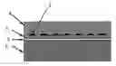
FIG. 1 illustrates the cross section of the InGaAlN multilayer structure grown on a Si substrate in accordance with embodiment 1 of the present invention.
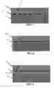
FIG. 2 illustrates the cross section of an InGaAlN multilayer structure grown on a Si substrate in accordance with embodiment 2 of the present invention.
FIG. 3 illustrates the cross section of an InGaAlN multilayer structure grown on a Si substrate in accordance with embodiment 3 of the present invention.
In the figures, label “1” refers to a Si substrate, label “2” refers to a metal transition layer, label “3” refers to an Mg masking layer, label “4” refers to an InGaAlN layer, label “5” refers to a first InGaAlN layer, and label “6” refers to a second InGaAlN layer.
DETAILED DESCRIPTION OF EMBODIMENTS
The following description uses three embodiment examples to further describe methods provided by the present invention.
Embodiment 1
A Si (111) substrate 1 is cleaned and placed inside the reaction chamber of a metal-organic-chemical-vapor-deposition (MOCVD) machine. First, the surface of substrate 1 is thermally processed using H2 for 5 minutes under high temperature. Then, the chamber temperature is lowered to below 720° C. A 0.5-mono-atomic-layer-thick of Mg mask layer 3 is deposited using bis(cyclopentadienyl)magnesium (Cp2Mg) as the source. The Mg mask layer only covers part of the surface of the Si substrate, and the covered area is between 10% and 90% of the total surface area. Subsequently, a thin layer of Al, i.e., the metal transition layer 2, and an AlN buffer layer are deposited under the same chamber temperature of 720° C. In the end, the chamber temperature is raised to 1050° C., and a 3 μm thick GaN layer, i.e., the InGaAlN semiconductor layer 4, is deposited.
Embodiment 2:
A Si (111) substrate 1 is cleaned and placed inside the reaction chamber of an MOCVD machine. First, substrate 1 is thermally processed using H2 for 5 minutes under high temperature, then the chamber temperature is lowered to below 900° C., and a thin layer of Ti, i.e., the metal transition layer 2, is deposited. Subsequently, a mono-atomic layer of Mg is deposited to form the Mg mask layer 3, wherein the Mg mask layer only covers part of the surface of the metal transition layer and the covered area is between 10% and 90% of the total surface area. Afterwards, an AlN buffer layer is deposited while the chamber temperature is kept at 880° C. In the end, the chamber temperature is raised to 1030° C., and a 3 μm thick GaN layer, i.e., the InGaAlN semiconductor layer 4, is deposited.
Embodiment 3:
A (111) Si substrate 1 is cleaned and placed inside the reaction chamber of an MOCVD machine. First, substrate 1 is thermally processed using H2 for 5 minutes under high temperature, then the chamber temperature is lowered to below 800° C., and a thin layer of Al/Ti alloy, i.e., the metal transition layer 2, is deposited. An AlN buffer layer is deposited while the chamber temperature is kept at 800° C. Afterwards, the chamber temperature is raised to 1030° C., and a 0.5 μm thick first GaN layer, i.e., the first InGaAlN semiconductor layer 5, is deposited on the AlN layer. The thickness of the first InGaAlN semiconductor layer can be between one mono-atomic layer and 3 μm. Subsequently, a two- mono-atomic-layer-thick Mg is deposited on the first GaN layer under the same chamber temperature to form Mg mask layer 3, wherein the Mg mask layer only covers part of the surface of the first InGaAlN semiconductor layer, and the covered area is between 10% and 90% of the total surface area. Then, a 2 μm thick GaN layer doped with Si, a 5-period InGaN/GaN multiple-quantum-well (MQW), and a 0.1 μm thick GaN layer doped with Mg, i.e., the second InGaAlN semiconductor layer 6, are deposited sequentially.
Claims
What is claimed is:1. A method for fabricating InGaAlN thin film on a silicon substrate, the method comprising:
forming an Mg mask layer on the Si substrate;
forming a metal transition layer on said Mg mask layer; and
forming an InGaAlN semiconductor layer on said metal transition layer;
wherein said Mg mask layer only covers part of the surface of said Si substrate, and wherein the covered area is between 10% and 90% of the total surface area.
2. The method of claim 1,
wherein said metal transition layer comprises an Al layer.
3. The method claim 1,
wherein said metal transition layer comprises a Ti layer.
4. The method of claim 1,
wherein said metal transition layer comprises an Al/Ti alloy layer.
5. The method of claim 1, further comprising:
forming a buffer layer after the formation of said metal transition layer and before the formation of said InGaAlN semiconductor layer.
6. The method of claim 5,
wherein said buffer layer comprises an AlN layer.
7. A method for fabricating InGaAlN thin film on a silicon substrate, the method comprising:
forming a metal transition layer on a Si substrate;
forming an Mg mask layer on said metal transition layer; and
forming an InGaAlN semiconductor layer on said Mg mask layer;
wherein said Mg mask layer only covers part of the surface of said metal transition layer, and wherein the covered area is between 10% and 90% of the total surface area.
8. The method of claim 7,
wherein said metal transition layer comprises an Al layer.
9. The method of claim 7,
wherein said metal transition layer comprises a Ti layer.
10. The method of claim 7,
wherein said metal transition layer comprises an Al/Ti alloy layer.
11. The method of claim 7, further comprising:
forming a buffer layer after the formation of said metal transition layer and before the formation of said InGaAlN semiconductor layer.
12. The method of claim 11,
wherein said buffer layer comprises an AlN layer.
13. A method for fabricating InGaAlN thin film on a silicon substrate, the method comprising:
forming a metal transition layer on a Si substrate;
forming a first InGaAlN semiconductor layer on said metal transition layer;
forming an Mg mask layer on said first InGaAlN semiconductor layer; and
forming a second InGaAlN semiconductor layer on said Mg mask layer;
wherein said Mg mask layer only covers part of the surface of said first InGaAlN semiconductor layer, and wherein the covered area is between 10% and 90% of the total surface area.
14. The method of claim 13,
wherein said metal transition layer comprises an Al layer.
15. The method of claim 13,
wherein said metal transition layer comprises a Ti layer.
16. The method of claim 13,
wherein said metal transition layer comprises an Al/Ti alloy layer.
17. The method of claim 13,
wherein the thickness of said first InGaAlN semiconductor layer is between 1 mono-atomic layer and 3 μm.
18. The method of claim 13, further comprising:
forming a buffer layer after the formation of said metal transition layer and before the formation of said first InGaAlN semiconductor layer.
19. The method of claim 18,
wherein said buffer layer comprises an AlN layer.
Images & Drawings included:
Sources:
- United States Patent and Trademark Office - verify current appl. status at the USPTO↗
Recent applications in this class:
- » 20250293026 2025-09-18
HIGH-POWER CARBON HARDMASK DEPOSITION AND CHARGE DISSIPATION - » 20250226216 2025-07-10
METALLIZATION STRUCTURE FOR COUPLING BOILING ENHANCED LAYER TO SUBSTRATE IN A COOLING SYSTEM - » 20240145242 2024-05-02
METHOD OF BLOCKING DIELECTRIC SURFACES USING BLOCKING MOLECULES TO ENABLE SELECTIVE EPI DEPOSITION - » 20220020587 2022-01-20
Method of manufacturing a semiconductor structure - » 20210175077 2021-06-10
Nonpolar or semipolar group III-nitride substrates - » 20190164756 2019-05-30
Source and drain formation using self-aligned processes - » 20140377963 2014-12-25
Patterning for selective area deposition - » 20120138132 2012-06-07
Silicon wafer based structure for heterostructure solar cells - » 20110186816 2011-08-04
SEMICONDUCTOR DEVICE WAFER, SEMICONDUCTOR DEVICE, DESIGN SYSTEM, MANUFACTURING METHOD AND DESIGN METHOD - » 20100218813 2010-09-02
Silicon wafer based structure for heterostructure solar cells
Recent applications for this Assignee:
- » 20110298005 2011-12-08
METHOD FOR FABRICATING AN N-TYPE SEMICONDUCTOR MATERIAL USING SILANE AS A PRECURSOR - » 20110147705 2011-06-23
SEMICONDUCTOR LIGHT-EMITTING DEVICE WITH SILICONE PROTECTIVE LAYER - » 20110133159 2011-06-09
SEMICONDUCTOR LIGHT-EMITTING DEVICE WITH PASSIVATION IN P-TYPE LAYER - » 20110049540 2011-03-03
Method for fabricating robust light-emitting diodes - » 20110031472 2011-02-10
Semiconductor light-emitting device with a highly reflective ohmic-electrode - » 20110006319 2011-01-13
Gallium nitride light-emitting device with ultra-high reverse breakdown voltage - » 20110001120 2011-01-06
Semiconductor light-emitting device with double-sided passivation - » 20100219394 2010-09-02
Method for fabricating a low-resistivity ohmic contact to a p-type III-V nitride semiconductor material at low temperature - » 20100207096 2010-08-19
Method for fabricating highly reflective ohmic contact in light-emitting devices - » 20100176404 2010-07-15
Method for fabricating high-power light-emitting diode arrays