Forming vias using sacrificial material
US20090004841A1
2009-01-01
11/824,212
2007-06-29
✅ Patent granted
US 7,727,886 B2
2010-06-01
-
-
Ha Tran T Nguyen | Daniel Whalen
2028-01-08
Abstract:
In one embodiment, the present invention includes a method for forming a sacrificial material layer, patterning it to obtain a first patterned sacrificial material layer, embedding the first patterned sacrificial material layer into a dielectric material, treating the first patterned sacrificial material layer to remove it to thus provide a patterned dielectric layer having a plurality of openings in which vias may be formed. Other embodiments are described and claimed.
Inventors:
- Lakshmi Supriya 10 🇺🇸 Chandler, AZ, United States
- Omar J. Bchir 10 🇺🇸 Phoenix, AZ, United States
Assignee:
- INTEL CORPORATION 47,158 🇺🇸 Santa Clara, CA, United States
Interested in similar patents?
Get notified when new applications in this technology area are published.
Classification:
H05K3/0017 » CPC main
Apparatus or processes for manufacturing printed circuits; Working of insulating substrates or insulating layers Etching of the substrate by chemical or physical means
H05K3/0017 » CPC main
Apparatus or processes for manufacturing printed circuits; Working of insulating substrates or insulating layers Etching of the substrate by chemical or physical means
H01L21/486 » CPC further
Processes or apparatus adapted for the manufacture or treatment of semiconductor or solid state devices or of parts thereof; Manufacture or treatment of semiconductor devices or of parts thereof the devices having at least one potential-jump barrier or surface barrier, e.g. PN junction, depletion layer or carrier concentration layer; Manufacture or treatment of parts, e.g. containers, prior to assembly of the devices, using processes not provided for in a single one of the subgroups -; Conductive parts; Leads on or in insulating or insulated substrates, e.g. metallisation Via connections through the substrate with or without pins
H01L21/76802 » CPC further
Processes or apparatus adapted for the manufacture or treatment of semiconductor or solid state devices or of parts thereof; Manufacture or treatment of devices consisting of a plurality of solid state components formed in or on a common substrate or of parts thereof; Manufacture of integrated circuit devices or of parts thereof; Manufacture of specific parts of devices defined in group; Applying interconnections to be used for carrying current between separate components within a device comprising conductors and dielectrics characterised by the formation and the after-treatment of the dielectrics, e.g. smoothing by forming openings in dielectrics
H05K3/4644 » CPC further
Apparatus or processes for manufacturing printed circuits; Manufacturing multilayer circuits by building the multilayer layer by layer, i.e. build-up multilayer circuits
H05K3/4644 » CPC further
Apparatus or processes for manufacturing printed circuits; Manufacturing multilayer circuits by building the multilayer layer by layer, i.e. build-up multilayer circuits
H05K2203/083 » CPC further
Indexing scheme relating to apparatus or processes for manufacturing printed circuits covered by; Treatments involving gases Evaporation or sublimation of a compound, e.g. gas bubble generating agent
H05K2203/083 » CPC further
Indexing scheme relating to apparatus or processes for manufacturing printed circuits covered by; Treatments involving gases Evaporation or sublimation of a compound, e.g. gas bubble generating agent
H05K2203/1105 » CPC further
Indexing scheme relating to apparatus or processes for manufacturing printed circuits covered by; Treatments characterised by their effect, e.g. heating, cooling, roughening Heating or thermal processing not related to soldering, firing, curing or laminating, e.g. for shaping the substrate or during finish plating
H05K2203/308 » CPC further
Indexing scheme relating to apparatus or processes for manufacturing printed circuits covered by; Details of processes not otherwise provided for in - Sacrificial means, e.g. for temporarily filling a space for making a via or a cavity or for making rigid-flexible PCBs
H05K2203/308 » CPC further
Indexing scheme relating to apparatus or processes for manufacturing printed circuits covered by; Details of processes not otherwise provided for in - Sacrificial means, e.g. for temporarily filling a space for making a via or a cavity or for making rigid-flexible PCBs
H01L21/44 IPC
Processes or apparatus adapted for the manufacture or treatment of semiconductor or solid state devices or of parts thereof; Manufacture or treatment of semiconductor devices or of parts thereof the devices having at least one potential-jump barrier or surface barrier, e.g. PN junction, depletion layer or carrier concentration layer the devices having semiconductor bodies not provided for in groups, , , and with or without impurities, e.g. doping materials Manufacture of electrodes on semiconductor bodies using processes or apparatus not provided for in groups -
H01L21/4763 IPC
Processes or apparatus adapted for the manufacture or treatment of semiconductor or solid state devices or of parts thereof; Manufacture or treatment of semiconductor devices or of parts thereof the devices having at least one potential-jump barrier or surface barrier, e.g. PN junction, depletion layer or carrier concentration layer the devices having semiconductor bodies not provided for in groups, , , and with or without impurities, e.g. doping materials; Treatment of semiconductor bodies using processes or apparatus not provided for in groups to change their surface-physical characteristics or shape, e.g. etching, polishing, cutting Deposition of non-insulating, e.g. conductive -, resistive -, layers on insulating layers; After-treatment of these layers
Description
BACKGROUND
Semiconductor devices are typically formed on a semiconductor die, which is then packaged in a package including a substrate. Substrate capacity and cost is a concern for the microelectronics industry. A substrate can include so-called vias, which are conductive structures to connect different metal layers in the substrate. As advances occur, the cost for laser drilling vias is increasing due to the increasing number of vias and decreasing size of the vias, which forces the innovation of new laser technologies. Due to the increasing number of vias, the throughput time of substrate manufacturing is increased.
Substrates can be formed of organic material including a core and multiple layers of patterned copper separated by dielectric polymer and interconnected by vias. The vias can be formed by carbon dioxide (CO2) laser drilling. This process can be time consuming, and limited to via diameters greater than about 50 microns. Further, practical concerns such as laser via to pad alignment and manufacturing throughput time restrict substrate design to a single via diameter per buildup (BU) layer.
BRIEF DESCRIPTION OF THE DRAWINGS
FIG. 1 is a cross-section view of a substrate in accordance with an embodiment of the present invention.
FIGS. 2A-2D are process flow diagrams of a method in accordance with one embodiment of the present invention.
FIGS. 3A-3E are process flow diagrams of a method in accordance with another embodiment of the present invention
DETAILED DESCRIPTION
In various embodiments, microvias may be formed in a substrate such as a package substrate or other such substrate using sacrificial materials. While the scope of the present invention is not limited in this regard, such microvias may have diameters of less than approximately 30 microns and up to greater than approximately 120 microns, in some embodiments. In this way, the need for other methods of forming microvias such as using laser techniques can be avoided. In different implementations, sacrificial material may be patterned into shapes that the microvias will take. Then a process to embed the sacrificial material into a dielectric may be performed. The sacrificial material may then be removed, leaving openings in the dielectric. These openings may then be used to form microvias, e.g., by plating of a conductive material such as a metal, by an electroless or electrolytic plating process.
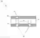
Referring now to FIG. 1, shown is a cross-section view of a substrate in accordance with an embodiment of the present invention. As shown in FIG. 1, substrate 10 may include a plurality of conductive planes 25, which in some embodiments may be copper (Cu) planes. Between conductive planes 25, dielectric layers may be present, such as formed using a polymer. Contacts may be made between conductive plates 25 by a plurality of microvias 30. In various embodiments, the area for the microvias may be formed using a sacrificial material in accordance with an embodiment of the present invention.
In various embodiments, a core material 40 may be a polymer or other dielectric material, which can be reinforced with glass fibers. Connections may be made through core material 40 by a plurality of plated through holes (PTHs) 45. Above core material 40, conductive planes may be present with dielectric layers 50 separating them. Microvias 30 and 55 are formed in the BU dielectric layers to make electrical connections between the metal layers in the buildup, and are typically metallized using an electroless or electrolytic deposition technique. Microvias 30 and 55, which are typically formed by laser drilling may instead be formed in accordance with an embodiment of the present invention. Although shown as a core-type package, the scope of the present invention is not limited in this regard and other embodiments may be used in a coreless substrate.
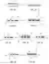
Referring now to FIGS. 2A-2D, shown is a process flow of a method in accordance with one embodiment of the present invention. As shown in FIG. 2A, a sacrificial material 110 may be patterned in a desired manner. A number of different sacrificial materials may be used, where a stimulus to later remove the material may either be thermal, light, microwave, or any other method. When using a thermal stimulus, the phase change (sublimation) temperature may range from room temperature to approximately 400° Celsius (C). Examples of such materials may include, but are not limited to, naphthalene and its derivatives (sublimes slowly at room temperature but may be made to sublime faster at higher temperatures, e.g., approximately 50° C.), camphor (or other terpene based systems), polycarbonates (and its derivatives) (sublimation temperature of ˜200° C.), poly(norbornene) and derivatives (sublimation temperature of ˜400° C.). The materials may also be made photosensitive by adding photoinitiators such as, but not limited to Irgacure 819, Irgacure 369 etc. By using such materials, they may be placed on desired regions simply by photopatterning. The sacrificial material may be deposited by spin-coating, printing or other methods.
Various photolithography or other processes may be performed to obtain a desired pattern of sacrificial material 110. Then sacrificial material 110 may be embedded within a dielectric 115. A wide variety of dielectric polymers may be used. Examples of dielectric polymers include thermoplastics, such as polyimides, polyesters, polyamides, and polyolefins, and thermosets, such as epoxies and bismaleimides. A wide variety of methods may be used to place a uniform dielectric coating, including vacuum lamination, spin coating, and other methods known in the art. In various embodiments, a lamination or solvent casting of dielectric 115 on sacrificial material 110 may be performed to embed sacrificial material 110 within dielectric 115, as shown in FIG. 2B. In one embodiment, the sacrificial material is polycarbonate and the dielectric material is a polyimide. The polycarbonate is patterned analogous to a metal pattern on a substrate such that it can be easily removed. The polyimide film is taken slightly above the glass transition temperature (Tg) such that it softens and is pressed onto the patterned polycarbonate, such that it is embedded into the film. The polycarbonate embedded dielectric film is laminated onto the substrate. In another embodiment, the sacrificial material is patterned by photolithography, etching or other methods on a surface, from which it may be easily removed. The dielectric polymer is poured over the patterned sacrificial material and solvent cast to form a film with the sacrificial material embedded in it. Alternatively, the sacrificial material may be patterned directly on the substrate and the dielectric solvent cast on the substrate.
To position a sacrificial material where microvias are desired to be located, a deposition process may be performed to apply dielectric 115 including sacrificial material 110 onto a substrate. More specifically, as shown in FIG. 2C, a substrate 100, which may be a package substrate or other substrate, may have conductive interconnects 120, which may be Cu pads or lines to provide interconnections to lower layers (not shown in FIG. 2C) of substrate 100. Accordingly, dielectric layer 115 may be deposited above substrate 100 as shown in FIG. 2C, e.g., by a lamination process. Then to eliminate sacrificial material 110, a given treatment process may be performed such as an ultraviolet (UV) treatment or a thermal treatment to release sacrificial material 110, resulting in the structure shown in FIG. 2D, which is a cross section view of a substrate including openings for formation of microvias. Of course, the microvias may then be metallized by a plating process.
FIGS. 3A-3E show a similar method for forming microvias using sacrificial materials. However, note that various differences in the processes exist. In the embodiment of FIG. 3A, a sacrificial material 220 is deposited onto a substrate 200 that includes patterned conductive interconnects 210, such as patterned Cu pads/lines, although other metals such as aluminum, silver, gold and others may be used. In various embodiments, sacrificial material 220 may be coated onto substrate 200. In one embodiment, the sacrificial material is modified poly(norbornene) with a photoinitiator. The sacrificial material is coated onto the patterned substrate by spin-coating. Then sacrificial material 220 may be patterned using photolithography in connection with a mask 225, as shown in FIG. 3B. After such UV treatment, sacrificial material 220 is patterned as shown in FIG. 3C. Then deposition of a dielectric material 230 may be performed. For example, a dielectric film is laminated onto the patterned sacrificial material. Finally, another treatment such as a thermal or UV treatment may be performed to eliminate sacrificial material 220, as shown in FIG. 3E in which a plurality of openings are provided within dielectric material 230 to enable formation of microvias. While shown with these particular processes in the embodiments of FIGS. 2A-2D and 3A-3E, the scope of the present invention is not limited in this regard.
While the present invention has been described with respect to a limited number of embodiments, those skilled in the art will appreciate numerous modifications and variations therefrom. It is intended that the appended claims cover all such modifications and variations as fall within the true spirit and scope of this present invention.
Claims
What is claimed is:1. A method comprising:
forming a sacrificial material layer;
patterning the sacrificial material layer to obtain a first patterned sacrificial material layer;
embedding the first patterned sacrificial material layer into a dielectric material;
depositing the dielectric material onto a first side of a core material, the core material including a plurality of conductive interconnections on the first side;
treating the core material to remove the first patterned sacrificial material layer to provide a patterned dielectric layer having a plurality of openings, the openings corresponding to the removed first patterned sacrificial material layer; and
forming a plurality of vias in the plurality of openings, wherein each of the vias contacts a corresponding one of the plurality of conductive interconnections.
2. The method of claim 1, wherein the sacrificial material layer comprises a camphor or polycarbonate material, and wherein the sacrificial material layer is formed by spin-coating or printing.
3. The method of claim 2, wherein embedding the first patterned sacrificial material layer comprises laminating the dielectric material on the first patterned sacrificial material layer, the dielectric material comprising a polymer material.
4. The method of claim 1, wherein treating the core material comprises a thermal treatment or an ultraviolet (UV) treatment and wherein the sacrificial material layer includes a photosensitive material.
5. The method of claim 1, further comprising plating a plurality of plated through holes in the core material to provide contact to the plurality of conductive interconnections prior to depositing the dielectric material.
6. The method of claim 5, further comprising:
forming a second sacrificial material layer;
patterning the second sacrificial material layer to obtain a second patterned sacrificial material layer and embedding the second patterned sacrificial material layer into a second dielectric material;
depositing the second dielectric material onto a second side of the core material; and
removing the second patterned sacrificial material layer to form a second plurality of vias.
7. The method of claim 1, wherein the sacrificial material layer includes a polycarbonate material and the dielectric material includes a polyimide, and wherein the polycarbonate is pressed onto the first patterned sacrificial material layer.
8. The method of claim 7, further comprising plating the vias in the plurality of openings.
9. A method comprising:
applying a sacrificial material layer on a substrate having a plurality of interconnections therein;
patterning the sacrificial material layer to obtain a first patterned sacrificial material layer;
depositing a dielectric material above the first patterned sacrificial material layer;
treating the substrate to remove the first patterned sacrificial material layer to obtain a patterned dielectric layer having a plurality of openings, the openings corresponding to the removed first patterned sacrificial material layer; and
forming microvias in the plurality of openings.
10. The method of claim 9, further comprising contacting corresponding ones of the plurality of interconnections with the microvias.
11. The method of claim 9, wherein applying the sacrificial material layer comprises coating sacrificial material onto the substrate.
12. The method of claim 9, wherein treating the substrate comprises a thermal treatment or an ultraviolet (UV) treatment.
13. The method of claim 9, further comprising applying the sacrificial material on a core material having a plurality of plated through holes within the core material to contact the microvias.
14. The method of claim 9, further comprising spin coating sacrificial material onto the substrate, the sacrificial material comprising modified poly(norbornene) and a photoinitiator, and laminating the dielectric material onto the sacrificial material layer.
Images & Drawings included:
Sources:
- United States Patent and Trademark Office - verify current appl. status at the USPTO↗
Similar patent applications:
Recent applications in this class:
- » 20240414849 2024-12-12
METHOD OF MANUFACTURING PRINTED CIRCUIT BOARD - » 20230209719 2023-06-29
Method of manufacturing printed circuit board - » 20190132956 2019-05-02
Method for manufacturing insulated circuit board, insulated circuit board, and thermoelectric conversion module - » 20190116673 2019-04-18
System for direct writing on an uneven surface of a workpiece that is covered with a radiation sensitive layer using exposures having different focal planes - » 20180092218 2018-03-29
RESIN COMPOSITION, PREPREG, METAL-FOIL-CLAD LAMINATE, RESIN SHEET, AND PRINTED WIRING BOARD - » 20170034919 2017-02-02
Method for producing an electronic device - » 20150382472 2015-12-31
Printed circuit board and manufacturing method thereof - » 20150366068 2015-12-17
Touch panel and its manufacturing method - » 20150351248 2015-12-03
Method for manufacturing substrate gap supporter - » 20150313021 2015-10-29
Display panel motherboard and manufacturing method thereof
Recent applications for this Assignee:
- » 20250294866 2025-09-18
GATE CUT CONFINED WITHIN GATE TRENCH - » 20250294846 2025-09-18
BACKSIDE CROSS-COUPLE INTERCONNECTS - » 20250294835 2025-09-18
ELONGATED VERTICAL STRUCTURES OF CHANNEL MATERIALS - » 20250294827 2025-09-18
CO-INTEGRATION OF GATE-ALL-AROUND DEVICES WITH DIFFERENT NUMBERS OF NANORIBBONS - » 20250294818 2025-09-18
TRANSISTOR DESIGNS FOR FLOATING BODY MEMORY - » 20250294781 2025-09-18
MAGNETIC CORE INDUCTORS ON PACKAGE SUBSTRATES - » 20250294777 2025-09-18
INTEGRATED CIRCUIT DEVICE WITH MEMORY ARRAY AND SHARED GAIN ELEMENT - » 20250293985 2025-09-18
RECEIVER-BASED PRECISION CONGESTION CONTROL - » 20250293860 2025-09-18
PRESERVATION OF CONFIDENTIALITY AND INTEGRITY OF MODELS DURING EXECUTION - » 20250293706 2025-09-18
LOW-RANK DECOMPOSITION-BASED HARDWARE COMPRESSION OF MATRICES AND TENSORS