CIRCUIT BOARD
US20090071702A1
2009-03-19
11/869,758
2007-10-10
Abstract:
A circuit board (10) for reducing a variation in impedance of signal traces thereon includes a first signal plane (30) and a second signal plane (50). The first signal plane includes a first signal trace (31) arranged thereon. The first signal trace has a first width. The second signal plane includes a plurality of second signal traces (51) arranged thereon. An orthographic projection of the first signal trace onto the second signal plane crosses the second signal traces. A width of the first signal trace at positions where the orthographic projection thereof onto the second signal plane at the intersections with the second signal traces transitions to a second width less than the first width of the first signal trace.
Assignee:
- HONG FU JIN PRECISION INDUSTRY (ShenZhen) CO., LTD 200 🇹🇼 Shenzhen City, Taiwan
- HON HAI PRECISION INDUSTRY CO., LTD. 620 🇹🇼 Taipei Hsien, Taiwan
Interested in similar patents?
Get notified when new applications in this technology area are published.
Classification:
H05K1/025 » CPC main
Printed circuits; Details; Electrical arrangements not otherwise provided for; High frequency adaptations Impedance arrangements, e.g. impedance matching, reduction of parasitic impedance
H05K1/025 » CPC main
Printed circuits; Details; Electrical arrangements not otherwise provided for; High frequency adaptations Impedance arrangements, e.g. impedance matching, reduction of parasitic impedance
H05K2201/09245 » CPC further
Indexing scheme relating to printed circuits covered by; Shape and layout; Shape and layout details of conductors; Conductive traces Crossing layout
H05K2201/09245 » CPC further
Indexing scheme relating to printed circuits covered by; Shape and layout; Shape and layout details of conductors; Conductive traces Crossing layout
H05K2201/09727 » CPC further
Indexing scheme relating to printed circuits covered by; Shape and layout; Shape and layout details of conductors covering at least two types of conductors provided for in - Varying width along a single conductor; Conductors or pads having different widths
H05K2201/09727 » CPC further
Indexing scheme relating to printed circuits covered by; Shape and layout; Shape and layout details of conductors covering at least two types of conductors provided for in - Varying width along a single conductor; Conductors or pads having different widths
Description
BACKGROUND
1. Field of the Invention
The present invention relates to circuit boards, and more particularly to a circuit board with a signal trace having a proper variation in impedance thereof.
2. Description of Related Art
Circuit boards, such as printed circuit boards (PCBs) are widely used in conventional electronic devices, for mounting electronic components of the electronic devices thereon and supplying electric connections among the electronic components. To achieve compactness of the PCB, electronic devices have become more complicated. Thereby it is important to ensure the signal quality of the circuit board.
FIG. 1 shows a configurable view of signal traces of a conventional circuit board 10′, which has a signal trace 11′ and a plurality of signal traces 13′ arranged on two different signal planes of the circuit board 10′ respectively. Widths of the signal trace 11′ and the signal traces 13′ are uniform. At positions where an orthographic projection of the signal trace 11′ crosses the signal traces 13′, the impedance of the signal trace 11′ will be reduced too much. For example, an original width of the signal trace 11′ is 5 mil (1 mil=0.0254 mm), if where the orthographic projection of the signal trace 11′ crosses the signal traces 13′ is perpendicular, the impedance of the signal trace 11′ will be reduced by 8.4 ohms from 52.2 ohms to 43.8 ohms; if the orthographic projection of the signal trace 11′ crosses the signal traces 13′ at an angle of 45 degrees, the impedance of the signal trace 11′ will be reduced by 7.9 ohms from 52.2 ohms to 44.3 ohms. The large variations in impedance may affect the signal quality of the circuit board 10′.
What is needed, therefore, is a circuit board having a smaller variation in impedance of a signal trace for improving signal quality.
SUMMARY
A circuit board for reducing a variation in impedance of signal traces thereon includes a first signal plane and a second signal plane. The first signal plane includes a first signal trace arranged thereon. The first signal trace has a first width. The second signal plane includes a plurality of second signal traces arranged thereon. An orthographic projection of the first signal trace onto the second signal plane crosses the second signal traces. A width of the first signal trace at positions where the orthographic projection thereof onto the second signal plane at the intersections with the second signal traces transitions to a second width less than the first width of the first signal trace.
Other advantages and novel features of the present invention will become more apparent from the following detailed description of a preferred embodiment when taken in conjunction with the accompanying drawings, in which:
BRIEF DESCRIPTION OF THE DRAWINGS
FIG. 1 is a view of signal trace configuration of a conventional circuit board;
FIG. 2 is a schematic view of a circuit board in accordance with an embodiment of the present invention;
FIG. 3 is a view of signal trace configuration of the circuit board of FIG. 2; and
FIG. 4 is a view of signal trace configuration in another embodiment of the circuit board of FIG. 2.
DETAILED DESCRIPTION
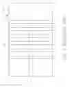
Referring to FIG. 2, a circuit board 10 of an embodiment of the present invention includes a ground plane 70, a first media plane 20, a first signal plane 30, a second media plane 40, and a second signal plane 50. The first media plane 20 is disposed between the ground plane 70 and the first signal plane 30, and the second media plane 40 is disposed between the first signal plane 30 and the second signal plane 50.
Referring also to FIG. 3, a first signal trace 31 is arranged on the first signal plane 30 for transmitting signals. A plurality of parallel second signal traces 51 is arranged in an area on the second signal plane 50 at regular intervals for transmitting signals. The first signal trace 31 has a first width. An orthographic projection of the first signal trace 31 on the second signal plane 50 crosses each of the second signal traces 51 perpendicularly. The width of the first signal trace 31 transitions to a narrower second width near or at the point where the projection enters the area of the seconds signal traces 51 and transitions back to the first width near or at the point where the projection leaves the area of the second signal traces 51.
For example, if the first width of the first signal trace 31 is 5 mil (1 mil=0.0254 mm), the impedance of the first signal trace 31 is 52.2 ohms. In this embodiment, if the width of the first signal trace 31 where its projection crosses the second signal traces 51 is reduced to 4 mil, the impedance of the first signal trace 31 will be reduced to 48.2 ohms, a reduction of only 4 ohms, thereby ensuring better signal quality of the circuit board 10.
Referring to FIG. 4, this embodiment is similar to the first embodiment except that second signal traces 51′ are turned so that an orthographic projection of a first signal trace 31′ crosses the second signal traces 51′ at a 45 degrees angle.
As in the first embodiment, if a first width of the first signal trace 31′ is 5 mil, the impedance of the first signal trace 31′ is 52.2 ohms, and the width of the first signal trace 31′ transitions to 4 mil, as before, the impedance is reduced to 48.8 ohms. In this embodiment the reduction is only 3.4 ohms. Thus, ensuring the signal quality of the circuit board 10.
It should be noted that the transitions between the first and second widths of the embodiments are gradually but can varied according to need in other embodiments.
According to the above, when an orthographic projection of one signal trace onto another signal plane of the circuit board 10 crosses the signal traces arranged on the other signal plane at an angle of 90 degrees or 45 degrees, a width of the one signal trace will be reduced, thereby decreasing the variation in impedance of the one signal trace to ensure the signal quality of the circuit board 10.
Wherein the first and second signal traces 31, 31′, 51, 51′ can be arranged on different signal planes of the circuit board 10 respectively. In addition, when the orthographic projection of one signal trace onto another signal plane crosses the signal traces arranged on the other signal plane at other angles, particularly from 30 degrees to 90 degrees, the width of the one signal trace may be reduced to improve the variation in impedance of the one signal trace, thereby ensuring the signal quality of the circuit board.
It is to be understood, however, that even though numerous characteristics and advantages of the present invention have been set forth in the foregoing description, together with details of the structure and function of the invention, the disclosure is illustrative only, and changes may be made in detail, especially in matters of shape, size, and arrangement of parts within the principles of the invention to the full extent indicated by the broad general meaning of the terms in which the appended claims are expressed.
Claims
What is claimed is:1. A circuit board comprising:
a first signal plane comprising a first signal trace arranged thereon, the first signal trace having a first width; and
a second signal plane comprising a plurality of second signal traces arranged thereon, an orthographic projection of the first signal trace onto the second signal plane crossing the second signal traces, wherein a width of the first signal trace at positions where the orthographic projection thereof onto the second signal plane at the intersections with the second signal traces transitions to a second width less than the first width of the first signal trace.
2. The circuit board as described in claim 1, wherein a width of the first signal trace at positions where the orthographic projection on the second signal plane between two adjacent second signal traces is equal to the second width.
3. The circuit board as described in claim 2, wherein the orthographic projection of the first signal trace onto the second signal plane crosses the second signal traces at an angle from 30 degrees to 90 degrees.
4. The circuit board as described in claim 1, wherein a media plane is disposed between the first signal plane and the second plane.
5. A circuit board comprising:
a first signal plane having a first signal trace arranged thereon; and
a second signal plane having a plurality of second signal traces arranged thereon, an orthographic projection of the first signal trace onto the second signal plane crossing the second signal traces, a width of the segments of the first signal trace corresponding to where the orthographic projection falls on the second signal plane at the intersections with each second signal trace being equal to that of where the orthographic projection of other segments of the first signal trace fall on the second signal plane between two adjacent second signal traces, and being less than a width of the remaining segments of the first signal trace.
6. The circuit board as claimed in claim 5, wherein the orthographic projection of the first signal trace onto the second signal plane crosses the second signal traces at an angle from 30 degrees to 90 degrees.
7. The circuit board as claimed in claim 5, wherein a media plane is disposed between the first signal plane and the second plane.
8. The circuit board as claimed in claim 5, wherein the plurality of second signal traces is arranged on the second signal plane at regular intervals, and parallel to each other.
9. The circuit board as claimed in claim 5, wherein the width of the first signal trace transitions gradually between segments of different widths.
10. A circuit board comprising:
a dielectric layer;
a first circuit layer formed on the dielectric layer, the first circuit layer having a first signal trace, the first signal trace having a first portion having a first width, and a second portion having a second width, the second width being less than the first width; and
a second circuit layer formed on an opposite side of the dielectric layer to the first circuit layer, the second circuit layer having a plurality of second signal traces, an orthographic projection of the second portion of the first signal trace onto a main plane of the second circuit layer intersecting the second signal traces.
11. The circuit board as claimed in claim 10, wherein a width of the joint section between the first and second portions of the first signal trace progressively increases from the second portion to the first portion.
12. The circuit board as claimed in claim 10, wherein the orthographic projection of second portion of the first signal trace onto the second signal plane intersects the second signal traces at an angle in the range from 30 degrees to 90 degrees.
Images & Drawings included:


Sources:
- United States Patent and Trademark Office - verify current appl. status at the USPTO↗
Similar patent applications:
- » 20220135767
Resin composition for circuit board, molded body for circuit board, layered body for circuit board, and circuit board - » 20140000941
Method for integrating an electronic component into a printed circuit board or a printed circuit board intermediate product, and printed circuit board or printed circuit board intermediate product - » 20120152592
Method for manufacturing printed circuit board, method for manufacturing printed circuit board assembly sheet, printed circuit board, and printed circuit board assembly sheet - » 20130302651
Battery pack including circuit board assembly having first circuit board connected to terminals and second circuit board connected to first circuit board - » 20230383030
MODIFIED FLUORORESIN MATERIAL, MATERIAL FOR CIRCUIT BOARD, LAMINATE FOR CIRCUIT BOARD, CIRCUIT BOARD, AND METHOD FOR PRODUCING MODIFIED FLUORORESIN MATERIAL - » 20050254218
Printed circuit board with improved heat dissipation efficiency, electronic apparatus having printed circuit board with improved heat dissipation efficiency, CRT display device having printed circuit board with improved heat dissipation efficiency, and recording/reproducing device or video display device incorporating recording/reproducing device having printed circuit board with improved heat dissipation efficiency - » 20230043114
Circuit board, circuit board connection structure, and method of manufacturing circuit board connection structure - » 20060217462
Flame-retardant epoxy resin composition, and electronic device, laminated circuit board, multilayered circuit board and printed circuit board using the flame-retardant epoxy resin composition - » 20200120795
METHOD FOR MANUFACTURING PRINTED CIRCUIT BOARD, PRINTED CIRCUIT BOARD AND DRIVE CIRCUIT BOARD - » 20130044448
Method for Mounting a Component to an Electric Circuit Board, Electric Circuit Board and Electric Circuit Board Arrangement
Recent applications in this class:
- » 20250168971 2025-05-22
TRACE WIDTH MODULATION - » 20250142715 2025-05-01
SYSTEMS AND METHOD FOR IMPEDANCE MATCHING ACROSS SUBASSEMBLIES - » 20250048539 2025-02-06
ULTRAVIOLET GLUE-CONTROLLED IMPEDANCE - » 20250040035 2025-01-30
Electronic Circuit For A Vehicle - » 20250040034 2025-01-30
REFLECTIVE CANCELLATIONS IN A CONNECTOR WIPE OF A SURFACE MOUNT CONNECTOR - » 20250040033 2025-01-30
REFLECTIVE CANCELLATIONS IN A CONNECTOR WIPE - » 20240314925 2024-09-19
TRANSMISSION LINE POWER DIVIDERS AND POWER COMBINERS WITH MATCHED PORTS - » 20230262880 2023-08-17
Circuit board structure - » 20230133827 2023-05-04
Transmission module, electronic unit, and electronic device - » 20230065980 2023-03-02
Multi-level printed circuit boards and memory modules including the same
Recent applications for this Assignee:
- » 20130279120 2013-10-24
SHELL FOR FIXING MAIN BOARD THERETO AND ELECTRONIC DEVICE HAVING SAME - » 20130262885 2013-10-03
Power supply device for solid state drive - » 20130234776 2013-09-12
Circuit for testing motherboard - » 20130168338 2013-07-04
SUPPORTING APPARATUS - » 20130163207 2013-06-27
HEAT SINK - » 20130141036 2013-06-06
CHARGEABLE CASE OF ELECTRONIC DEVICE AND CHARGING SYSTEM - » 20130120928 2013-05-16
Server with expansion card - » 20130110461 2013-05-02
Computing device and method for generating measurement program of product - » 20130100609 2013-04-25
CONTAINER DATA CENTER - » 20130100602 2013-04-25
Server with improved layout