Method of forming strain-causing layer for MOS transistors and process for fabricating strained MOS transistors
US20090111272A1
2009-04-30
11/926,852
2007-10-29
✅ Patent granted
US 7,727,903 B2
2010-06-01
-
-
Charles D Garber | Andre′ C Stevenson
2027-12-10
Abstract:
A method of forming a strain-causing layer for MOS transistors is provided, which is applied to a substrate having a plurality of gate structures of the MOS transistors thereon. A non-conformal stressed film that is thicker on the gate structures than between the gate structures is formed over the substrate. The non-conformal stressed film is then etched, without an etching mask thereon, to remove portions thereof between the gate structures and disconnect the stressed film between the gate structures. At least one extra stressed film may be further formed over the substrate, wherein each extra stressed film has the same type of stress as the above stressed film and is connected or disconnected between the gate structures.
Inventors:
- PEI-LIN KUO 5 🇹🇼 Taichung City, Taiwan
- Huo-Tieh Lu 2 🇹🇼 Taipei, Taiwan
- Jin-sheng Yang 3 🇹🇼 Hsinchu, Taiwan
- Pei-Lin Kuo 2 🇹🇼 Taichung, Taiwan
Assignee:
- UNITED MICROELECTRONICS CORP. 1,463 🇹🇼 Hsinchu, Taiwan
Interested in similar patents?
Get notified when new applications in this technology area are published.
Classification:
H01L29/7833 » CPC main
Semiconductor devices adapted for rectifying, amplifying, oscillating or switching, or capacitors or resistors with at least one potential-jump barrier or surface barrier, e.g. PN junction depletion layer or carrier concentration layer; Details of semiconductor bodies or of electrodes thereof; Multistep manufacturing processes therefor; Types of semiconductor device ; Multistep manufacturing processes therefor controllable by only the electric current supplied, or only the electric potential applied, to an electrode which does not carry the current to be rectified, amplified or switched; Unipolar devices, e.g. field effect transistors; Field effect transistors with field effect produced by an insulated gate with lightly doped drain or source extension, e.g. LDD MOSFET's; DDD MOSFET's
H01L21/31 IPC
Processes or apparatus adapted for the manufacture or treatment of semiconductor or solid state devices or of parts thereof; Manufacture or treatment of semiconductor devices or of parts thereof the devices having at least one potential-jump barrier or surface barrier, e.g. PN junction, depletion layer or carrier concentration layer the devices having semiconductor bodies comprising elements of Group IV of the Periodic System or AB compounds with or without impurities, e.g. doping materials; Treatment of semiconductor bodies using processes or apparatus not provided for in groups - to form insulating layers thereon, e.g. for masking or by using photolithographic techniques ; After treatment of these layers; Selection of materials for these layers
Description
BACKGROUND OF THE INVENTION
1. Field of Invention
This invention relates to a semiconductor process, and more particularly relates to a method of forming a strain-causing layer for MOS transistors and a process for fabricating strained MOS transistors.
2. Description of Related Art
As the linewidth of semiconductor device is much reduced and the requirement on the device speed increasingly gets higher, the strained-silicon technology is provided. In a metal-oxide-semiconductor (MOS) process utilizing the strained-silicon technology in the prior art, a stressed film is formed over the MOS transistors to cause strains in the channels regions thereof.
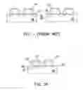
FIG. 1 illustrates a conventional stressed film for MOS transistors, wherein each transistor is based on a semiconductor substrate 100 and includes a gate structure 110. When the MOS transistors are NMOS transistors with n-type S/D regions 105, a tensile-stressed film 120 is formed over them. When the transistors are PMOS transistors with p-type S/D regions 105′, a compressive-stressed film 120′ is formed over them.
However, because the conventional stressed film 120/120′ is connected between two neighboring gate structures 110, the stresses for the two transistors counteract each other thereat, as indicated by the pair of opposite arrows, so that the strain caused is reduced and the performances of the transistors are lowered. This issue is important especially when the distance between the two neighboring gate structures 110 is small.
SUMMARY OF THE INVENTION
Accordingly, this invention provides a method of forming a strain-causing layer for MOS transistors.
This invention also provides a process for forming strained MOS transistors, which is based on the method of forming a strain-causing layer of this invention.
The method of forming a strain-causing layer of this invention is described below. A substrate with a plurality of gate structures of MOS transistors thereon is provided. A non-conformal stressed film that is thicker on the gate structures than between the gate structures is formed over the substrate. The non-conformal stressed film is etched, without an etching mask thereon, to remove portions thereof between the gate structures and disconnect the stressed film between the gate structures.
In an embodiment of the above method, at least one extra stressed film may be further formed over the substrate, wherein each extra stressed film has the same type of stress as the stressed film and is connected or disconnected between the gate structures.
The process for forming strained MOS transistors of this invention is based on the above method of forming a strain-causing layer. After the strain-causing layer is formed, a dielectric layer is formed over the substrate covering the stressed film.
Since the strain-causing layer (or at least the first stressed film in a strain-causing layer of multiple stressed films in an embodiment of this invention) is disconnected between the gate structures, the stresses for two neighboring transistors don't counteract each other so that the strains caused in the transistor channel regions are increased and the performances of the transistors are improved as compared with the prior art.
It is to be understood that both the foregoing general description and the following detailed description are exemplary, and are intended to provide further explanation of the invention as claimed.
BRIEF DESCRIPTION OF THE DRAWINGS
FIG. 1 illustrates a conventional stressed film for MOS transistors.
FIGS. 2A-2B illustrate a process for forming strained MOS transistors according to a first embodiment of this invention, wherein a method of forming a strain-causing layer for MOS transistors according to the first embodiment is also shown.
FIG. 3 illustrates a later part of a process for forming strained MOS transistors according to a second embodiment of this invention.
FIG. 4 illustrates a later part of a process for forming strained MOS transistors according to a third embodiment of this invention.
DESCRIPTION OF EMBODIMENTS
FIGS. 2A-2B illustrate a process for forming strained MOS transistors according to a first embodiment of this invention, wherein a method of forming a strain-causing layer for MOS transistors according to the first embodiment is also shown.
Referring to FIG. 2A, a semiconductor substrate 200 having a plurality of gate structures 210 of MOS transistors thereon is provided, wherein the material of the substrate 200 may be single-crystal silicon or SiGe. A gate structure 210 may include a gate dielectric film 212, a gate 214 on the gate dielectric film 212 and a spacer 216 on the sidewall of the gate 214, wherein the gate 214 may include doped polysilicon. The S/D regions 205 of the MOS transistors have also been formed in the substrate 200.
Then, a non-conformal stressed film 220 that is thicker on the gate structures 210 than between the gate structures 210 is formed. When the MOS transistors are NMOS transistors with n-type S/D regions 205, the stressed film 220 is a tensile-stressed one; when the transistors are PMOS transistors with p-type S/D regions 205, the stressed film 220 is a compressive-stressed one. In addition, the material of the non-conformal stressed film 220 may be silicon nitride. A deposition recipe allowing formation of a non-conformal stressed film thicker at specific portions can be found in the prior art, and is thus not exemplified here.
Moreover, an etching stop layer may be formed over the substrate 200 before the non-conformal stressed film 220 is formed for protecting the substrate 200 in the later etching step. As the material of the non-conformal stressed film 220 is silicon nitride, the material of the etching stop layer may be silicon oxide, for example.
Referring to FIG. 2B, the non-conformal stressed film 220 is etched without an etching mask thereon, wherein the etching is preferably anisotropic etching for the sake of controllability. Since the non-conformal stressed film 220 (FIG. 2A) is thicker on the gate structures 210 than between the gate structures 210, portions thereof on the gate structures 210 remains as portions thereof between the gate structures 210 are removed, thus disconnecting the stressed film 220 between the gate structures 210. The stressed film 220a as a single-film strain-causing layer disconnected between the gate structures 210 may be cured in option to increase the stress thereof, wherein the curing may be UV-light curing or other type of curing. Then, an inter-layer dielectric (ILD) layer 230 is formed covering the stressed film 220a.
Moreover, after the above stressed film 220a is formed, at least one extra stressed film may be further formed over the substrate 200, wherein each extra stressed film has the same type of stress as the stressed film 220a and is connected or disconnected between the gate structures 210. When the stressed film is tensile- or compressive-stressed, the at least one extra stressed film is also tensile- or compressive-stressed. The stressed film 220a and the at least one extra stressed film constitute a multi-film strain-causing layer. In addition, the stressed film 220a and the extra stressed film(s) may all include silicon nitride. Two such embodiments are described below.
FIG. 3 illustrates a later part of a process for forming strained MOS transistors according to a second embodiment of this invention.
Referring to FIG. 3, after the stressed film 220a is formed, an extra stressed film 300 is formed over the substrate 200 covering the gate structures 210 and the stressed film 220a. The extra stressed film 300 has the same type of stress as the stressed film 220a but is connected between the gate structures 210. Thereafter, an ILD layer 230 is formed covering the resulting structures.
In the second embodiment, the non-contiguous stressed film 220a and the extra stressed film 300 connected between the gate structures 210 together constitute a strain-causing layer. The stressed film 220a and the extra stressed film 300 are both tensile-stressed films in cases of NMOS transistors or both compressive-stressed films in cases of PMOS transistors, and may both include silicon nitride.
FIG. 4 illustrates a later part of a process for forming strained MOS transistors according to a third embodiment of this invention.
Referring to FIG. 4, after the stressed film 220a is formed, an extra stressed film 400 is formed covering the gate structures 210 and the stressed film 220a. The extra stressed film 400 has the same type of stress as the stressed film 220a, and is also disconnected between the gate structures 210 like the stressed film 220a.
The extra stressed film 400 may be formed in the same manner in which the stressed film 220a is formed. Specifically, a non-conformal extra stressed film that is thicker on the gate structures 210 than between the gate structures 210 like the stressed film shown in FIG. 2A is formed over the substrate 200, and then the non-conformal extra stressed film is etched, without an etching mask thereon, to remove portions thereof between the gate structures 210 and obtain the extra stressed film 400. Then, an ILD layer 230 is formed covering the resulting structures.
In the third embodiment, the stressed film 220a and the extra stressed film 400 both disconnected between the gate structures 210 together constitute a strain-causing layer. The stressed film 220a and the extra stressed film 400 are both tensile-stressed films in cases of NMOS transistors or compressive-stressed films in cases of PMOS transistors, and may both include silicon nitride.
Since the strain-causing layer (or at least the first stressed film in a multi-film strain-causing layer as in the second embodiment of this invention) is disconnected between the gate structures, the stresses for two neighboring transistors don't counteract each other so that the strains caused in the transistor channel regions are increased and the performances of the transistors are improved as compared with the prior art.
This invention has been disclosed above in the preferred embodiments, but is not limited to those. It is known to persons skilled in the art that some modifications and innovations may be made without departing from the spirit and scope of this invention. Hence, the scope of this invention should be defined by the following claims.
Claims
What is claimed is:1. A method of forming a strain-causing layer for MOS transistors, applied to a substrate with a plurality of gate structures of MOS transistors thereon, and comprising:
forming over the substrate a non-conformal stressed film that is thicker on the gate structures than between the gate structures; and
etching, without an etching mask, the non-conformal stressed film to remove portions thereof between the gate structures and disconnect the stressed film between the gate structures.
2. The method of claim 1, wherein an etching stop layer is formed over the substrate before the non-conformal stressed film is formed.
3. The method of claim 1, further comprising curing the stressed film disconnected between the gate structures to increase a stress thereof.
4. The method of claim 3, wherein the curing comprises UV-light curing.
5. The method of claim 1, wherein the stressed film is a tensile-stressed film or a compressive-stressed film.
6. The method of claim 1, wherein the etching comprises anisotropic etching.
7. The method of claim 1, wherein the stressed film comprises silicon nitride.
8. The method of claim 1, further comprising:
forming at least one extra stressed film over the substrate after the stressed film is disconnected between the gate structures, wherein each extra stressed film has the same type of stress as the stressed film and is connected or disconnected between the gate structures.
9. The method of claim 8, wherein when an extra stressed film is disconnected between the gate structures, forming the extra stressed film comprises:
forming over the substrate a non-conformal extra stressed film that is thicker on the gate structures than between the gate structures; and
etching, without an etching mask, the non-conformal extra stressed film to remove portions thereof between the gate structures and disconnect the extra stressed film between the gate structures.
10. The method of claim 8, wherein the stressed film and the at least one extra stressed film are tensile-stressed films or compressive-stressed films.
11. The method of claim 8, wherein the stressed film and the at least one extra stressed film comprise silicon nitride.
12. A process for forming strained MOS transistors, comprising:
providing a substrate with a plurality of gate structures of MOS transistors thereon;
forming over the substrate a non-conformal stressed film that is thicker on the gate structures than between the gate structures;
etching, without an etching mask, the non-conformal stressed film to remove portions of the stressed film between the gate structures and disconnect the stressed film between the gate structures; and
forming a dielectric layer over the substrate covering the stressed film.
13. The process of claim 12, further comprising forming an etching stop layer over the substrate before the non-conformal stressed film is formed.
14. The process of claim 12, further comprising curing the stressed film to increase a stress thereof, after the stressed film is disconnected between the gate structures but before the dielectric layer is formed.
15. The process of claim 14, wherein the curing comprises UV-light curing.
16. The process of claim 12, wherein the MOS transistors are NMOS transistors and the stressed film is a tensile-stressed film.
17. The process of claim 12, wherein the MOS transistors are PMOS transistors and the stressed film is a compressive-stressed film.
18. The process of claim 12, wherein the etching comprises anisotropic etching.
19. The process of claim 12, wherein the stressed film comprises silicon nitride.
20. The process of claim 12, further comprising:
forming at least one extra stressed film over the substrate after the non-conformal stressed film is disconnected between the gate structures but before the dielectric layer is formed, wherein each extra stressed film has the same type of stress as the stressed film and is connected or disconnected between the gate structures.
21. The process of claim 20, wherein when an extra stressed film is disconnected between the gate structures, forming the extra stressed film comprises:
forming over the substrate a non-conformal extra stressed film that is thicker on the gate structures than between the gate structures; and
etching, without an etching mask, the non-conformal extra stressed film to remove portions thereof between the gate structures and disconnect the extra stressed film between the gate structures.
22. The process of claim 20, wherein the stressed film and the at least one extra stressed film are tensile-stressed films or compressive-stressed films.
23. The process of claim 20, wherein the stressed film and the at least one extra stressed film comprise silicon nitride.
Images & Drawings included:


Sources:
- United States Patent and Trademark Office - verify current appl. status at the USPTO↗
Recent applications in this class:
- » 20250072035 2025-02-27
SEMICONDUCTOR DEVICE AND METHOD FOR FABRICATING THE SAME - » 20240405125 2024-12-05
BURIED CHANNEL SEMICONDUCTOR DEVICE INCLUDING ENERGY BARRIER MODULATION REGION(S) - » 20240379845 2024-11-14
TRANSISTOR STRUCTURE AND METHODS OF FORMATION - » 20240355924 2024-10-24
SEMICONDUCTOR DEVICE HAVING MOS TRANSISTOR FOR EFFICIENT STRESS TRANSFER - » 20240304723 2024-09-12
TWO-ROTATION GATE-EDGE DIODE LEAKAGE REDUCTION FOR MOS - » 20240282857 2024-08-22
SEMICONDUCTOR DEVICE, PHOTOELECTRIC CONVERSION DEVICE, AND ELECTRONIC APPARATUS - » 20240222505 2024-07-04
DESIGNS FOR SILICON CARBIDE MOSFETs - » 20240105844 2024-03-28
NATIVE NMOS DEVICE AND MANUFACTURING METHOD THEREOF - » 20240047579 2024-02-08
SEMICONDUCTOR DEVICE - » 20240014319 2024-01-11
SEMICONDUCTOR STRUCTURE AND TRANSISTOR STRUCTURE
Recent applications for this Assignee:
- » 20250293183 2025-09-18
SEMICONDUCTOR DEVICE - » 20250285993 2025-09-11
MANUFACTURING METHOD OF SEMICONDUCTOR STRUCTURE INCLUDING SEAL RING STRUCTURE - » 20250266368 2025-08-21
METHOD OF FORMING SEMICONDUCTOR DEVICE, ZERO-LAYER OVERLAY MARK AND METHOD OF FORMING THE SAME - » 20250241057 2025-07-24
SEMICONDUCTOR DEVICE AND MANUFACTURING METHOD THEREOF - » 20250239279 2025-07-24
MEMORY DEVICE AND METHOD OF CONTROLLING EQUIVALENT RESISTANCE OF BIT LINE OR SOURCE LINE CORRESPONDING TO WORD LINE OF THE MEMORY DEVICE - » 20250237942 2025-07-24
PHOTOMASK DESIGN METHOD, SEMICONDUCTOR MANUFACTURING PROCESS, AND SEMICONDUCTOR STRUCTURE - » 20250237675 2025-07-24
JIG AND METHOD FOR GRINDING PROBE PINS OF PROBE CARD - » 20250234575 2025-07-17
SEMICONDUCTOR DEVICE AND MANUFACTURING METHOD THEREOF - » 20250233038 2025-07-17
SEMICONDUCTOR STRUCTURE AND MANUFACTURING METHOD THEREOF - » 20250218693 2025-07-03
CAPACITOR STRUCTURE AND MANUFACTURING METHOD THEREOF