Method for calculating out an optimum arrangement pitch between each two LED chip package units
US20090213378A1
2009-08-27
12/285,178
2008-09-30
✅ Patent granted
US 7,815,346 B2
2010-10-19
-
-
Sang Nguyen
2029-01-03
Abstract:
A method for calculating out an optimum arrangement pitch between each two LED chip package units, including: providing a backlight module with a predetermined brightness value and a predetermined material information that a customer needs; determining what brightness level and amount of LED chip package units need to be used by a designer according to the brightness value and the material information of the backlight module; and dividedly arranging the LED chip package units determined by the designer on a light-entering area of the backlight module in order to define what the optimum arrangement pitch between each two LED chip package units is.
Inventors:
- BILY WANG 65 🇹🇼 HSINCHU CITY, Taiwan
- Shih-Yu Wu 10 🇹🇼 Banciao City, Taiwan
- Wen-Kuei Wu 11 🇹🇼 Hukou Township, Taiwan
- BILY WANG 37 🇹🇼 HSINCHU, Taiwan
- Shih-Yu Wu 7 🇹🇼 Banciao, Taiwan
- Wen-Kuei Wu 8 🇹🇼 Hukou Township, Hsinchu County, Taiwan
Assignee:
- HARVATEK CORPORATION 54 🇹🇼 Hsinchu, Taiwan
Interested in similar patents?
Get notified when new applications in this technology area are published.
Classification:
G01B11/14 » CPC main
Measuring arrangements characterised by the use of optical means for measuring distance or clearance between spaced objects or spaced apertures
G01B11/00 IPC
Measuring arrangements characterised by the use of optical means
F21V5/00 IPC
Refractors for light sources
G09G5/00 IPC
Control arrangements or circuits for visual indicators common to cathode-ray tube indicators and other visual indicators
Description
BACKGROUND OF THE INVENTION
1. Field of the Invention
The present invention relates to a method for arranging LED chip package units, and particularly relates to a method for calculating out an optimum arrangement pitch between each two LED chip package units.
2. Description of Related Art
In general, designers arrange LED chip package units of the prior art on a substrate according to their own experience. In other words, the designer defines the distance between each two LED chip package units in a backlight unit according to previous experience. However, the method of the prior art cannot determine the most suitable distances and also can easily produce man-made errors.
SUMMARY OF THE INVENTION
One particular aspect of the present invention is to provide a method for calculating out an optimum arrangement pitch between each two LED chip package units. The present invention can determine what brightness level and amount of LED chip package units need to be used by a designer according to the brightness value and the material information of the backlight module in order to define the optimum arrangement pitch between each two LED chip package units.
In order to achieve the above-mentioned aspects, the present invention provides a method for calculating out an optimum arrangement pitch between each two LED chip package units, including: providing a backlight module with a predetermined brightness value and a predetermined material information that a customer needs; determining what brightness level and amount of LED chip package units need to be used by a designer according to the brightness value and the material information of the backlight module; and dividedly arranging the LED chip package units determined by the designer on a light-entering area of the backlight module in order to define what the optimum arrangement pitch between each two LED chip package units is.
Hence, the present invention can accurately calculate out the optimum arrangement pitch between each two LED chip package units.
It is to be understood that both the foregoing general description and the following detailed description are exemplary, and are intended to provide further explanation of the invention as claimed. Other advantages and features of the invention will be apparent from the following description, drawings and claims.
BRIEF DESCRIPTION OF THE DRAWINGS
The various objects and advantages of the present invention will be more readily understood from the following detailed description when read in conjunction with the appended drawings, in which:
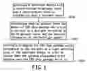
FIG. 1 is a flowchart of a method for calculating out an optimum arrangement pitch between each two LED chip package units of the present invention;
FIG. 2 is a side, schematic view of a backlight module of the present invention;
FIG. 3A is a schematic view of the first type of arrangement of LED chip package units; and
FIG. 3B is a schematic view of the second type of arrangement of LED chip package units.
DETAILED DESCRIPTION OF PREFERRED EMBODIMENTS
Referring to FIG. 1, the present invention provides a method for calculating out an optimum arrangement pitch between each two LED chip package units, including: providing a backlight module with a predetermined brightness value and a predetermined material information that a customer needs (S100); determining what brightness level and amount of LED chip package units need to be used by a designer according to the brightness value and the material information of the backlight module (S102); and dividedly arranging the LED chip package units determined by the designer on a light-entering area of the backlight module in order to define what the optimum arrangement pitch between each two LED chip package units is (S104).
Referring to FIGS. 2, 3A and 3B, the backlight module B is composed of a light emitting unit 10, a light guiding board 11, a reflective board 12, a diffusing board 13, a prism board 14, and an LED light polarizing board 15. In addition, the light emitting unit 10 is composed of the LED chip package units 100 determined by the designer, and light beams L generated from the light emitting unit 10 are directly projected onto the light guiding board 11 or are indirectly projected onto the light guiding board 11 via the reflective board 12.
Moreover, the reflective board 12 has a first reflective board 121 and a second reflective board 122. The light beams L generated from the light emitting unit 10 are reflected by the first reflective board 121, and the light beams L that have passed the light guiding board 11 are reflected by the second reflective board 122. In addition, the light guiding board 11 is disposed beside one side of the light emitting unit 10 for receiving the light beams L generated from the light emitting unit 10, the diffusing board 13 is disposed over the light guiding board 11, the prism board 14 is disposed over the diffusing board 13, and the LED light polarizing board 15 is disposed over the prism board 14.
Therefore, referring to FIG. 3A, the present invention provides a method for calculating out an optimum arrangement pitch between each two LED chip package units, including: firstly, providing a backlight module with a predetermined brightness value (5500 nits) and a predetermined material information such as the backlight module B of FIG. 2 that a customer needs; determining to use 27 LED chip package units 100 with 1200 mcd by a designer according to the brightness value and the material information of the backlight module B; and dividedly arranging the 27 LED chip package units 100 with 1200 mcd determined by the designer on a light-entering area of the backlight module B in order to define the optimum arrangement pitch (5.5 mm) between each two LED chip package units 100.
Therefore, referring to FIG. 3B, the present invention provides a method for calculating out an optimum arrangement pitch between each two LED chip package units, including: firstly, providing a backlight module with a predetermined brightness value (3600 nits) and a predetermined material information such as the backlight module B of FIG. 2 that a customer needs; determining to use 18 LED chip package units 100 with 1200 mcd by a designer according to the brightness value and the material information of the backlight module B; and dividedly arranging the 18 LED chip package units 100 with 1200 mcd determined by the designer on a light-entering area of the backlight module B in order to define the optimum arrangement pitch (8.5 mm) between each two LED chip package units 100.
In conclusion, the present invention can determine what brightness level and amount of LED chip package units need to be used by a designer according to the brightness value and the material information of the backlight module in order to define the optimum arrangement pitch between each two LED chip package units. Hence, the present invention can accurately calculate out the optimum arrangement pitch between each two LED chip package units.
Although the present invention has been described with reference to the preferred best molds thereof, it will be understood that the invention is not limited to the details thereof. Various substitutions and modifications have been suggested in the foregoing description, and others will occur to those of ordinary skill in the art. Therefore, all such substitutions and modifications are intended to be embraced within the scope of the invention as defined in the appended claims.
Claims
What is claimed is:1. A method for calculating out an optimum arrangement pitch between each two LED chip package units, comprising:
providing a backlight module with a predetermined brightness value and a predetermined material information that a customer needs;
determining what brightness level and amount of LED chip package units need to be used by a designer according to the brightness value and the material information of the backlight module; and
dividedly arranging the LED chip package units determined by the designer on a light-entering area of the backlight module in order to define what the optimum arrangement pitch between each two LED chip package units is.
2. The method as claimed in claim 1, wherein the backlight module is composed of a light emitting unit, a light guiding board, a reflective board, a diffusing board, a prism board, and an LED light polarizing board.
3. The method as claimed in claim 2, wherein the light emitting unit is composed of the LED chip package units determined by the designer, and light beams generated from the light emitting unit are directly projected onto the light guiding board or are indirectly projected onto the light guiding board via the reflective board.
4. The method as claimed in claim 2, wherein the reflective board has a first reflective board and a second reflective board, light beams generated from the light emitting unit are reflected by the first reflective board, and the light beams that have passed the light guiding board are reflected by the second reflective board.
5. The method as claimed in claim 2, wherein the light guiding board is disposed beside one side of the light emitting unit for receiving light beams generated from the light emitting unit, the diffusing board is disposed over the light guiding board, the prism board is disposed over the diffusing board, and the LED light polarizing board is disposed over the prism board.
Images & Drawings included:


Sources:
- United States Patent and Trademark Office - verify current appl. status at the USPTO↗
Recent applications in this class:
- » 20250277659 2025-09-04
METHOD FOR DETERMINING GAP AND DEVICE FOR DETERMINING GAP BETWEEN STEEL SHEETS IN RESISTANCE SPOT WELDING - » 20250237493 2025-07-24
Stringed Instrument Scanning System and Related Methods - » 20250207911 2025-06-26
DEPOSITION APPARATUS, MASK FOR DEPOSITION APPARATUS, AND METHOD OF MEASURING GAP BETWEEN MASK FOR DEPOSITION APPARATUS AND SUBSTRATE - » 20250172382 2025-05-29
KEY DEPRESSION AMOUNT SENSOR DEVICE - » 20250155234 2025-05-15
METHODS AND SYSTEMS OF OPTICAL INSPECTION OF ELECTRONIC DEVICE MANUFACTURING MACHINES - » 20250146809 2025-05-08
LIGHT FIELD DISPLAY METROLOGY - » 20250146808 2025-05-08
CLEARANCE MEASURING APPARATUS - » 20250109936 2025-04-03
PATTERN MEASUREMENT DEVICE, PATTERN MEASUREMENT PROGRAM, AND PATTERN MEASUREMENT METHOD - » 20250067557 2025-02-27
Method and Device for an Indirect Length Measurement - » 20250012561 2025-01-09
Optical Displacement Sensor
Recent applications for this Assignee:
- » 20230343666 2023-10-26
Packaging method and package structure - » 20220359451 2022-11-10
Semiconductor device with high heat dissipation efficiency - » 20210328111 2021-10-21
LED display screen module - » 20210305449 2021-09-30
Light source assembly, optical sensor assembly, and method of manufacturing a cell of the same - » 20210305313 2021-09-30
Light-emitting diode (LED) assembly and method of manufacturing an LED cell of the same - » 20200233627 2020-07-23
Movable display device - » 20200219856 2020-07-09
Display device - » 20200052171 2020-02-13
Light emitting diode assembly structure - » 20190189864 2019-06-20
Display device and light source module having high color conversion efficiency thereof - » 20190151530 2019-05-23
Enema device and method of using the same