METHOD FOR FABRICATION OF SEMICONDUCTOR DEVICE
US20100090219A1
2010-04-15
12/568,867
2009-09-29
Abstract:
A method of fabrication of a semiconductor device having low resistance in an interconnection line and the same coefficient of thermal expansion as a semiconductor substrate is disclosed. The method includes forming a nitride film over a semiconductor substrate including a bottom metal line and a top metal line connected to each other through a plurality of vias, forming a trench at a through-silicon via (TSV) region of the semiconductor substrate, filling the trench with a predetermined material to form a silicon film, exposing the silicon film using a photoresist pattern, ion-implanting a dopant into the exposed silicon film, and selectively performing laser annealing to the silicon film to diffuse only the dopant implanted into the silicon film.
Interested in similar patents?
Get notified when new applications in this technology area are published.
Classification:
H01L21/268 » CPC main
Processes or apparatus adapted for the manufacture or treatment of semiconductor or solid state devices or of parts thereof; Manufacture or treatment of semiconductor devices or of parts thereof the devices having at least one potential-jump barrier or surface barrier, e.g. PN junction, depletion layer or carrier concentration layer the devices having semiconductor bodies comprising elements of Group IV of the Periodic System or AB compounds with or without impurities, e.g. doping materials; Bombardment with radiation with high-energy radiation using electromagnetic radiation, e.g. laser radiation
H01L21/76898 » CPC further
Processes or apparatus adapted for the manufacture or treatment of semiconductor or solid state devices or of parts thereof; Manufacture or treatment of devices consisting of a plurality of solid state components formed in or on a common substrate or of parts thereof; Manufacture of integrated circuit devices or of parts thereof; Manufacture of specific parts of devices defined in group; Applying interconnections to be used for carrying current between separate components within a device comprising conductors and dielectrics formed through a semiconductor substrate
H01L23/481 » CPC further
Details of semiconductor or other solid state devices; Arrangements for conducting electric current to or from the solid state body in operation, e.g. leads, terminal arrangements ; Selection of materials therefor Internal lead connections, e.g. via connections, feedthrough structures
H01L2224/02372 » CPC further
Indexing scheme for arrangements for connecting or disconnecting semiconductor or solid-state bodies and methods related thereto as covered by; Means for bonding being attached to, or being formed on, the surface to be connected, e.g. chip-to-package, die-attach, "first-level" interconnects; Manufacturing methods related thereto; Bonding areas; Manufacturing methods related thereto; Redistribution layers [RDL] for bonding areas; Disposition of the redistribution layers connecting to a via connection in the semiconductor or solid-state body
H01L2224/03 » CPC further
Indexing scheme for arrangements for connecting or disconnecting semiconductor or solid-state bodies and methods related thereto as covered by; Means for bonding being attached to, or being formed on, the surface to be connected, e.g. chip-to-package, die-attach, "first-level" interconnects; Manufacturing methods related thereto; Bonding areas; Manufacturing methods related thereto Manufacturing methods
H01L2224/0401 » CPC further
Indexing scheme for arrangements for connecting or disconnecting semiconductor or solid-state bodies and methods related thereto as covered by; Means for bonding being attached to, or being formed on, the surface to be connected, e.g. chip-to-package, die-attach, "first-level" interconnects; Manufacturing methods related thereto; Bonding areas; Manufacturing methods related thereto; Structure, shape, material or disposition of the bonding areas prior to the connecting process Bonding areas specifically adapted for bump connectors, e.g. under bump metallisation [UBM]
H01L2224/05 » CPC further
Indexing scheme for arrangements for connecting or disconnecting semiconductor or solid-state bodies and methods related thereto as covered by; Means for bonding being attached to, or being formed on, the surface to be connected, e.g. chip-to-package, die-attach, "first-level" interconnects; Manufacturing methods related thereto; Bonding areas; Manufacturing methods related thereto; Structure, shape, material or disposition of the bonding areas prior to the connecting process of an individual bonding area
H01L2924/14 » CPC further
Indexing scheme for arrangements or methods for connecting or disconnecting semiconductor or solid-state bodies as covered by; Details of semiconductor or other solid state devices to be connected; Device type Integrated circuits
H01L29/04 IPC
Semiconductor devices adapted for rectifying, amplifying, oscillating or switching, or capacitors or resistors with at least one potential-jump barrier or surface barrier, e.g. PN junction depletion layer or carrier concentration layer; Details of semiconductor bodies or of electrodes thereof; Multistep manufacturing processes therefor; Semiconductor bodies ; Multistep manufacturing processes therefor characterised by their crystalline structure, e.g. polycrystalline, cubic or particular orientation of crystalline planes
H01L21/265 » CPC further
Processes or apparatus adapted for the manufacture or treatment of semiconductor or solid state devices or of parts thereof; Manufacture or treatment of semiconductor devices or of parts thereof the devices having at least one potential-jump barrier or surface barrier, e.g. PN junction, depletion layer or carrier concentration layer the devices having semiconductor bodies comprising elements of Group IV of the Periodic System or AB compounds with or without impurities, e.g. doping materials; Bombardment with radiation with high-energy radiation producing ion implantation
Description
The present application claims priority under 35 U.S.C. 119 to Korean Patent Application No. 10-2008-0099570 (filed on Oct. 10, 2008), which is hereby incorporated by reference in its entirety.
BACKGROUND
Packaging technology for integrated circuits has been developed to satisfy the demand for miniaturization and reliable mounting. Various related stack technologies have been developed to meet the demand for high performance and miniaturization of electronic products.
In the semiconductor industry, the term “stack” means that at least two chips or packages are stacked vertically. For a memory device, through the use of stack technology, it is possible to realize a product having a memory capacity twice or more that which can be realized in a semiconductor integration process. Also, in addition to the increase of a memory capacity, stack packages have an advantage in mount density and efficient use of a mounting surface. Therefore, the stack package is under accelerated research and development.
A structure using a through silicon via (TSV) has been proposed as an example of a stack package. A stack package using the TSV has a structure in which the TSV is formed in each chip. Physical and electrical connections between chips are made vertically by the TSV. The stack package is fabricated as follows.
A vertical hole is formed in a predetermined region of each chip at the wafer level, and an insulation film is formed over the surface of the vertical hole. A seed layer is formed over the insulation film, and the vertical hole is filled with an electrolyte, i.e., metal, by electroplating to form a TSV. Subsequently, the backside of the wafer is ground to expose the TSV. Then, the wafer is divided into individual chips by sawing, and at least two chips are vertically stacked on a substrate using the TSV. Subsequently, the top of the substrate, including the stacked chips, is molded, and a solder ball is mounted to the bottom of the substrate, to complete the fabrication of the stack package.
In a related stack package using such a TSV, however, the vertical hole is filled with an electrolyte, i.e., copper, to form the TSV. At this time, heat is generated, with the result that cracking occurs due to the difference in coefficient of thermal expansion between the silicon and the copper. Junction reliability is greatly deteriorated.
SUMMARY
Embodiments relate to a method of fabrication of a semiconductor device. More particularly, embodiments relate to a method of fabrication of a semiconductor device having low resistance in an interconnection line and the same coefficient of thermal expansion as a semiconductor substrate.
Embodiments relate to a method of fabrication of a semiconductor device which includes forming a nitride film over a semiconductor substrate including a bottom metal line and a top metal line connected to each other through a plurality of vias, forming a trench at a through silicon via (TSV) region of the semiconductor substrate, filling the trench with a predetermined material to form a silicon film, exposing the silicon film using a photoresist pattern to expose the silicon film and ion-implanting a dopant into the exposed silicon film, and selectively performing laser annealing to the silicon film to diffuse only the dopant constituting the silicon film.
Embodiments also relate to an apparatus configured to form a nitride film over a semiconductor substrate comprising a bottom metal line and a top metal line connected to each other through a plurality of vias, form a trench at a through-silicon via region of the semiconductor substrate, fill the trench with a predetermined material to form a silicon film, expose the silicon film using a photoresist pattern, ion-implant a dopant into the exposed silicon film, and selectively anneal the silicon film with a laser to diffuse only the dopant implanted into the silicon film.
DRAWINGS
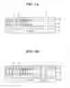
Example FIGS. 1A to 1F are views illustrating a method for fabrication of a semiconductor device according to embodiments.
DESCRIPTION
Example FIGS. 1A to 1F are views illustrating a method for fabrication of a semiconductor device according to embodiments. Processes are shown in order. Referring first to example FIG. 1A, a nitride film (plasma-enhanced(PE)-nitride) may be formed over a semiconductor substrate 100 including a top metal line 112 and a bottom metal line 114 having through silicon via (TSV) forming regions. The top metal line 112 and the bottom metal line 114 may be connected to each other through a plurality of vias 116.
A pre-metal dielectric (PMD) layer 102 may be formed between the bottom metal line 114 and the semiconductor substrate 100. A first inter metal dielectric (IMD) layer 104 may be formed between the top metal line 112 and the bottom metal line 114. A second IMD layer 106 may be formed together with the top metal line 112 over the first IMD layer 104. In other words, as shown in FIG. 1A, the second IMD layer 106 is formed in the same layer as the top metal line 112, over the first IMD layer 104.
Subsequently, a photoresist may be applied, and a first photoresist pattern to expose the TSV forming regions may be formed by exposure and development. The exposed TSV forming regions are etched, using the first photoresist pattern as an etching mask, to form a trench 120. The deep trench 120 may be formed to a predetermined depth in the semiconductor substrate 100 through the PMD layer 102, the first IMD layer 104, the second IMD layer 106, and the nitride film 110.
Subsequently, as shown in example FIG. 1B, the first photoresist pattern used as the etching mask may be removed by etching. An insulation film 122 may be formed over the entire surface of the nitride film 110, including the surface of the trench 120, to prevent diffusion of an electrolyte. The insulation film 122 may be formed of a nitride film or an oxide film by high-temperature dry etching or wet etching.
Subsequently, poly silicon or amorphous silicon (A-Si) may be deposited over the entire surface of the nitride film 110, including the insulation film 122 and the trench 120, by plasma enhanced chemical vapor deposition (PECVD) to fill the trench 120. The deposited poly silicon or A-Si may be flattened by chemical mechanical polishing (CMP), such that the insulation film 122 is exposed, to form a silicon film 124.
Subsequently, as shown in example FIG. 1C, a photoresist may be applied to the entire surface thereof, and a second photoresist pattern 126, designed to expose a region of the silicon film 124 corresponding to the TSV forming regions, may be formed by exposure and development. A dopant may be ion-implanted into the exposed silicon film 124 using the second photoresist pattern 126 as an ion implant mask. A group 3 element such as boron or a group 5 element may be used as the dopant, and the ion implantation may be performed with an energy of 11 B+15 to 350 KeV.
Subsequently, as shown in example FIG. 1D, laser annealing, such as eximer laser annealing, is performed for activation of the silicon film 124 to selectively diffuse only the dopant constituting the silicon film 124. The laser annealing may be performed at a wavelength of 1,000 to 1,500 nm and with an energy density of 2 J/cm2 to 10 J/cm2.
Since, unlike a related rapid thermal process (RTP), only the silicon film 124 is selectively annealed by the laser annealing, the metal lines and the oxide film do not substantially deteriorate. As a result, the resistance of the bottom metal line 114 and the top metal line 112 is lowered, and, at the same time, the coefficient of thermal expansion (CTE) as a general TSV is achieved.
As shown in example FIG. 1E, the portions of the nitride film 110 and the insulation film 122 corresponding to the top metal line 112 are selectively etched to form a pad opening 130 through which the top metal line 112 is partially exposed. As shown in example FIG. 1F, the pad opening 130 is filled with metal, and the remaining photoresist is removed to form a redistribution layer 132 to interconnect the silicon film 124 and a bump pad. Known subsequent processes may be performed to complete a semiconductor device.
As apparent from the above description, the method of fabrication of the semiconductor device according to embodiments selectively diffuses only the dopant constituting the TSV silicon through the laser annealing, thereby lowering resistance of the interconnection line and providing the same coefficient of thermal expansion as the semiconductor substrate and the poly silicon TSV.
It will be obvious and apparent to those skilled in the art that various modifications and variations can be made in the embodiments disclosed. Thus, it is intended that the disclosed embodiments cover the obvious and apparent modifications and variations, provided that they are within the scope of the appended claims and their equivalents.
Claims
What is claimed is:1. A method comprising:
forming a nitride film over a semiconductor substrate comprising a bottom metal line and a top metal line connected to each other through a plurality of vias;
forming a trench at a through-silicon via region of the semiconductor substrate;
filling the trench with a predetermined material to form a silicon film;
exposing the silicon film using a photoresist pattern;
ion-implanting a dopant into the exposed silicon film; and
selectively performing laser annealing to the silicon film to diffuse only the dopant implanted into the silicon film.
2. The method of claim 1, including:
selectively etching portions of a nitride film and an insulation film corresponding to the top metal line to form a pad opening through which the top metal line is partially exposed; and
filling the pad opening with metal to form a redistribution layer.
3. The method of claim 1, wherein the semiconductor substrate includes:
a pre-metal dielectric layer formed between the bottom metal line and the semiconductor substrate;
a first inter-metal dielectric layer formed between the top metal line and the bottom metal line; and
a second inter-metal dielectric layer formed in the same layer with the top metal line, over the first inter-metal dielectric layer.
4. The method of claim 1, including forming an insulation film over a surface of the trench after forming the trench.
5. The method of claim 4, wherein the insulation film is formed of an oxide film.
6. The method of claim 4, wherein the insulation film is formed of a nitride film.
7. The method of claim 1, wherein the silicon film is formed by depositing poly silicon.
8. The method of claim 7, including flattening the deposited poly silicon by chemical mechanical polishing.
9. The method of claim 1, wherein the silicon film is formed by plasma enhanced chemical vapor deposition.
10. The method of claim 1, wherein the silicon film is formed by depositing amorphous silicon by plasma enhanced chemical vapor deposition and flattening the deposited amorphous silicon by chemical mechanical polishing.
11. The method of claim 1, wherein the step of ion-implanting the dopant is performed with a group 3 element.
12. The method of claim 1, wherein the step of ion-implanting the dopant is performed with a group 5 element.
13. The method of claim 1, wherein the ion-implanting the dopant is performed with boron (B).
14. The method of claim 1, wherein the laser annealing is performed at a wavelength of 1,000 to 1,500 nm.
15. The method of claim 1, wherein the laser annealing is performed with an energy density of 2 J/cm2 to 10 J/cm2.
16. The method of claim 3, wherein the trench is formed through the pre-metal dielectric layer, the first inter-metal dielectric layer, the second inter-metal dielectric layer, and the nitride film.
17. An apparatus configured to:
form a nitride film over a semiconductor substrate comprising a bottom metal line and a top metal line connected to each other through a plurality of vias;
form a trench at a through-silicon via region of the semiconductor substrate;
fill the trench with a predetermined material to form a silicon film;
expose the silicon film using a photoresist pattern;
ion-implant a dopant into the exposed silicon film; and
selectively anneal the silicon film with a laser to diffuse only the dopant implanted into the silicon film.
18. The apparatus of claim 17, wherein the semiconductor substrate includes:
a pre-metal dielectric layer formed between the bottom metal line and the semiconductor substrate;
a first inter-metal dielectric layer formed between the top metal line and the bottom metal line; and
a second inter-metal dielectric layer formed in the same layer with the top metal line, over the first inter-metal dielectric layer, wherein the apparatus is configured to form the trench through the pre-metal dielectric layer, the first inter-metal dielectric layer, the second inter-metal dielectric layer, and the nitride film.
19. The apparatus of claim 17, configured to form the silicon film by depositing amorphous silicon by plasma enhanced chemical vapor deposition and flattening the deposited amorphous silicon by chemical mechanical polishing.
20. The apparatus of claim 17, configured to form the silicon film by depositing poly silicon by plasma enhanced chemical vapor deposition and flattening the deposited poly silicon by chemical mechanical polishing.
Images & Drawings included:


Sources:
- United States Patent and Trademark Office - verify current appl. status at the USPTO↗
Similar patent applications:
- » 20120112209
SILICON CARBIDE SUBSTRATE FABRICATION METHOD, SEMICONDUCTOR DEVICE FABRICATION METHOD, SILICON CARBIDE SUBSTRATE, AND SEMICONDUCTOR DEVICE - » 20080315254
Semiconductor device fabrication method, semiconductor device, and semiconductor layer formation method - » 20060043570
Substrate, semiconductor device, substrate fabricating method, and semiconductor device fabricating method - » 20050014377
Semiconductor device fabrication method and semiconductor device fabrication system for minimizing film-thickness variations - » 20080203440
Semiconductor device fabrication method and semiconductor device fabricated thereby - » 20060118952
Micro-hole plating method, gold bump fabrication method and semiconductor device fabrication method using the micro-hole plating method, semiconductor device - » 20060177743
Photomask, photomask fabrication method, and semiconductor device fabrication method - » 20070048890
Semiconductor device fabrication method and semiconductor device - » 20060084251
Plating method, semiconductor device fabrication method and circuit board fabrication method - » 20060084253
Plating method, semiconductor device fabrication method and circuit board fabrication method
Recent applications in this class:
- » 20250157823 2025-05-15
DICING METHOD AND RECORDING ELEMENT MANUFACTURING METHOD - » 20250140561 2025-05-01
PROCESSING METHOD OF WAFER - » 20250118561 2025-04-10
WORKPIECE PROCESSING METHOD - » 20250112048 2025-04-03
METHOD FOR PROCESSING WORKPIECE - » 20250105011 2025-03-27
LASER PROCESSING METHOD AND LASER PROCESSING DEVICE - » 20250095995 2025-03-20
SUBSTRATE PROCESSING METHOD AND SUBSTRATE PROCESSING SYSTEM - » 20250087490 2025-03-13
DEVICE CHIP MANUFACTURING METHOD - » 20250087489 2025-03-13
CHIP MANUFACTURING METHOD - » 20250054763 2025-02-13
LASER ANNEALING DEVICE, LASER ANNEALING METHOD, AND NON-TRANSITORY COMPUTER READABLE MEDIUM STORING LASER ANNEALING PROGRAM - » 20250006498 2025-01-02
LASER IRRADIATION APPARATUS, LASER IRRADIATION METHOD, AND METHOD FOR MANUFACTURING SEMICONDUCTOR DEVICE