PB-FREE SOLDER ALLOY
US20100092335A1
2010-04-15
12/521,655
2007-12-28
Abstract:
The present invention is provided to prevent the generation of whiskers via a lead (Pb)-free solder alloy. To achieve this objective, the present invention provides a Pb-free solder alloy including tin (Sn) as a first element and either boron (B) or beryllium (Be) as a second element.
Inventors:
- Dong Nyung Lee 5 🇰🇷 Seoul, South Korea
- Sang Beom Kim 3 🇰🇷 Daejeon-city, South Korea
- Kyoo Sik Kang 3 🇰🇷 Seoul, South Korea
Assignee:
- ILJIN COPPER FOIL CO., LTD. 2 🇰🇷 Iksan-city, South Korea
Interested in similar patents?
Get notified when new applications in this technology area are published.
Classification:
B23K35/262 » CPC further
Rods, electrodes, materials, or media, for use in soldering, welding, or cutting characterised by the composition or nature of the material; Selection of soldering or welding materials proper with the principal constituent melting at less than 400 degrees C Sn as the principal constituent
C22C13/00 » CPC main
Alloys based on tin
Description
TECHNICAL FIELD
The present invention relates to a solder alloy not containing lead (hereinafter, referred to as a Pb-free solder alloy), and more particularly, to a Pb-free solder alloy that generates no whiskers by including beryllium (Be) or boron (B).
BACKGROUND ART
Soldering is a technique of joining two or more members together by using a solder having a melting point of 450° C. or less. In soldering, only the solder is melted and a base material is not melted.
A conventional solder, used in soldering, is an alloy of lead (Pb) and tin (Sn). Such Pb—Sn solders mostly comprise 63% by weight of tin and have a eutectic composition of tin and Pb, and a melting point of 183° C., which does not thermally destroy electronic parts. In addition, the Pb—Sn solders have excellent wetability for the electrodes of ball grid arrays (BGAs) or the lands of printed circuit boards (PCBs) and thus reduce the number of soldering failures.
However, when electronic apparatuses using such Pb—Sn solders are disused, the Pb contained in these solders pollutes the environment. With the reinforcement of a restriction on the use of Pb, the Pb—Sn solders are becoming difficult to be used.
Accordingly, Pb-free solders containing no lead are recently in use. A compound obtained by adding Ag, Cu, Zn, In, Ni, Cr, Fe, Co, Ge, P, or Ga to a Sn—Ag based material, a Sn—Cu based material, a Sn—Bi based material, a Sn—Zn based material, or an alloy of each of the aforementioned materials is the main representative of Pb-free solder alloys.
A Sn—3Ag—0.5Cu compound from among Pb-free solders obtained by adding Cu to a Sn—Ag based material is good in terms of solderability, a joint strength, and high-resistant fatigability, and is thus currently used in soldering for many electronic apparatuses. The Sn—3Ag—0.5Cu compound is also used as a solder alloy for forming bumps and balls of BGAs.
However, when a Sn—Ag—Cu based Pb-free alloy is used as a solder for a long period of time, whiskers are prone to be formed on the surface of the solder. The whiskers are denoted by crystals that grow from the surface of the solder when the solder is joined with a different material and their components are diffused with each other. These whiskers are sensitive to heat and moisture. When these whiskers are formed on the surface of a solder alloy, an electrical short occurs within a circuit. Therefore, the durabilities of a BGA package and a flip-chip package are reduced.
DESCRIPTION OF THE DRAWINGS
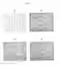
FIGS. 1A through 1D are scanning electron microscope (SEM) pictures of a surface of a specimen that has just been manufactured, a surface of the specimen subjected to a thermal shock test, a surface of the specimen subjected to a thermo-hydrostatic test, and a surface of the specimen that was left undisturbed at a normal temperature, respectively, according to a first experiment;
FIGS. 2A through 2D are SEM pictures of a surface of a specimen that has just been manufactured, a surface of the specimen subjected to a thermal shock test, a surface of the specimen subjected to a thermo-hydrostatic test, and a surface of the specimen that was left undisturbed at a normal temperature, respectively, under the same conditions as those of the first experiment, according to a second experiment;
FIGS. 3A through 3D are SEM pictures of a surface of a specimen that has just been manufactured, a surface of the specimen subjected to a thermal shock test, a surface of the specimen subjected to a thermo-hydrostatic test, and a surface of the specimen that was left undisturbed at a normal temperature, respectively, under the same conditions as those of the first experiment, according to a third experiment;
FIGS. 4A through 4D are SEM pictures of a surface of a specimen that has just been manufactured, a surface of the specimen subjected to a thermal shock test, a surface of the specimen subjected to a thermo-hydrostatic test, and a surface of the specimen that was left undisturbed at a normal temperature, respectively, under the same conditions as those of the first experiment, according to a fourth experiment;
FIGS. 5A through 5D are SEM pictures of a surface of a specimen that has just been manufactured, a surface of the specimen subjected to a thermal shock test, a surface of the specimen subjected to a thermo-hydrostatic test, and a surface of the specimen that was left undisturbed at a normal temperature, respectively, under the same conditions as those of the first experiment, according to a fifth experiment;
FIGS. 6A through 6D are SEM pictures of a surface of a specimen that has just been manufactured, a surface of the specimen subjected to a thermal shock test, a surface of the specimen subjected to a thermo-hydrostatic test, and a surface of the specimen that was left undisturbed at a normal temperature, respectively, under the same conditions as those of the first experiment, according to a sixth experiment;
FIGS. 7A through 7D are SEM pictures of a surface of a specimen that has just been manufactured, a surface of the specimen subjected to a thermal shock test, a surface of the specimen subjected to a thermo-hydrostatic test, and a surface of the specimen that was left undisturbed at a normal temperature, respectively, under the same conditions as those of the first experiment, according to a seventh experiment;
FIGS. 8A through 8D are SEM pictures of a surface of a specimen that has just been manufactured, a surface of the specimen subjected to a thermal shock test, a surface of the specimen subjected to a thermo-hydrostatic test, and a surface of the specimen that was left undisturbed at a normal temperature, respectively, under the same conditions as those of the first experiment, according to an eighth experiment;
FIGS. 9A through 9D are SEM pictures of a surface of a specimen that has just been manufactured, a surface of the specimen subjected to a thermal shock test, a surface of the specimen subjected to a thermo-hydrostatic test, and a surface of the specimen that was left undisturbed at a normal temperature, respectively, under the same conditions as those of the first experiment, according to a ninth experiment;
FIGS. 10A through 10D are SEM pictures of a surface of a specimen that has just been manufactured, a surface of the specimen subjected to a thermal shock test, a surface of the specimen subjected to a thermo-hydrostatic test, and a surface of the specimen that was left undisturbed at a normal temperature, respectively, under the same conditions as those of the first experiment, according to a tenth experiment;
FIGS. 11A through 11D are SEM pictures of a surface of a specimen that has just been manufactured, a surface of the specimen subjected to a thermal shock test, a surface of the specimen subjected to a thermo-hydrostatic test, and a surface of the specimen that was left undisturbed at a normal temperature, respectively, under the same conditions as those of the first experiment, according to an eleventh experiment;
FIGS. 12A through 12D are SEM pictures of a surface of a specimen that has just been manufactured, a surface of the specimen subjected to a thermal shock test, a surface of the specimen subjected to a thermo-hydrostatic test, and a surface of the specimen that was left undisturbed at a normal temperature, respectively, under the same conditions as those of the first experiment, according to a twelfth experiment;
FIGS. 13A through 13D are SEM pictures of a surface of a specimen that has just been manufactured, a surface of the specimen subjected to a thermal shock test, a surface of the specimen subjected to a thermo-hydrostatic test, and a surface of the specimen that was left undisturbed at a normal temperature, respectively, under the same conditions as those of the first experiment, according to a first comparative experiment;
FIGS. 14A through 14D are SEM pictures of a surface of a specimen that has just been manufactured, a surface of the specimen subjected to a thermal shock test, a surface of the specimen subjected to a thermo-hydrostatic test, and a surface of the specimen that was left undisturbed at a normal temperature, respectively, under the same conditions as those of the first experiment, according to a second comparative experiment;
FIGS. 15A through 15D are SEM pictures of a surface of a specimen that has just been manufactured, a surface of the specimen subjected to a thermal shock test, a surface of the specimen subjected to a thermo-hydrostatic test, and a surface of the specimen that was left undisturbed at a normal temperature, respectively, under the same conditions as those of the first experiment, according to a third comparative experiment;
FIGS. 16A through 16D are SEM pictures of a surface of a specimen that has just been manufactured, a surface of the specimen subjected to a thermal shock test, a surface of the specimen subjected to a thermo-hydrostatic test, and a surface of the specimen that was left undisturbed at a normal temperature, respectively, under the same conditions as those of the first experiment, according to a fourth comparative experiment;
FIGS. 17A through 17D are SEM pictures of a surface of a specimen that has just been manufactured, a surface of the specimen subjected to a thermal shock test, a surface of the specimen subjected to a thermo-hydrostatic test, and a surface of the specimen that was left undisturbed at a normal temperature, respectively, under the same conditions as those of the first experiment, according to a fifth comparative experiment; and
FIGS. 18A through 18D are SEM pictures of a surface of a specimen that has just been manufactured, a surface of the specimen subjected to a thermal shock test, a surface of the specimen subjected to a thermo-hydrostatic test, and a surface of the specimen that was left undisturbed at a normal temperature, respectively, under the same conditions as those of the first experiment, according to a sixth comparative experiment.
DETAILED DESCRIPTION OF THE INVENTION
Technical Problem
The present invention provides a Pb-free solder alloy that does not include lead (Pb) and also can prevent generation of whiskers.
Technical Solution
According to an aspect of the present invention, there is provided a Pb-free solder alloy comprising tin (Sn) as a first element and one of boron (B) or beryllium (Be) as a second element.
The second element of the Pb-free solder alloy may be 0.001 to 0.4% by weight of Be and the rest of the Pb-free solder alloy may be comprised of the first element and inevitable impurities.
The second element of the Pb-free solder alloy may be 0.003 to 0.5% by weight of B and the rest of the Pb-free solder alloy may be comprised of the first element and inevitable impurities.
The Pb-free solder alloy may further include copper (Cu) as a third element.
The third element may be 0.1 to 5.0% by weight.
The second element of the Pb-free solder alloy may be 0.001 to 0.4% by weight of Be and the rest of the Pb-free solder alloy may be comprised of the first element, the third element, and inevitable impurities.
The second element of the Pb-free solder alloy may be 0.003 to 0.5% by weight of B and the rest of the Pb-free solder alloy may be comprised of the first element, the third element, and inevitable impurities.
The Pb-free solder alloy may further comprise silver (Ag) as a fourth element.
The second element of the Pb-free solder alloy may be 0.001 to 0.4% by weight of Be and the rest of the Pb-free solder alloy may be comprised of one of a group of the first and fourth elements and inevitable impurities and a group of the first, third, and fourth elements and inevitable impurities.
The second element of the Pb-free solder alloy may be 0.003 to 0.5% by weight of B and the rest of the Pb-free solder alloy may be comprised of one of a group of the first and fourth elements and inevitable impurities and a group of the first, third, and fourth elements and inevitable impurities.
ADVANTAGEOUS EFFECTS
According to the present invention as described above, a Pb-free solder alloy capable of preventing generation of whiskers can be provided.
BEST MODE
As described above, a conventional Sn—Ag—Cu-based Pb-free solder has a disadvantage of generating whiskers on the surface thereof. However, the cause of the generation of the whiskers is not yet clearly revealed.
The inventors of the present invention paid attention to the fact that when a Pb—Sn solder is bonded to a pad formed of Cu, Cu is diffused faster than Sn on a bonding surface between the solder and the Cu pad.
In other words, since copper (Cu) is diffused faster than tin (Sn), which is a main component of the solder, between the solder and the Cu pad, the Cu is diffused in the direction of a grain boundary of the solder. Thereafter, an intermetallic compound with a Cu6Sn5 composition is formed in the solder.
The inventors of the present invention thought that a compressive stress applied by the intermetallic compound to the Sn of the solder can be removed by whiskers, which are single crystals having beard formations, growing from the surface of the solder where Sn is spread.
Accordingly, the inventors of the present invention tried to reduce the number of generations of a compressive stress within the Sn by preventing intermetallic diffusion via the insertion of a metal whose atoms are small into an interstitial site within the crystal structure of the Sn, consequently preventing the generation of whiskers.
Beryllium (Be) or boron (B) may be used as the metal with small atoms.
A Pb-free solder alloy according to the present invention is a Sn-based multi-element alloy that contains Sn as the main ions. Accordingly, the Pb-free solder alloy according to the present invention may contain at least 80% by weight of Sn.
As described above, the main object of the present invention is to prevent generation of whiskers within a Pb-free solder alloy. Particularly, the inventors of the present invention paid attention to Be or B as a material that can prevent the formation of a compressive stress within Sn crystals by preventing Sn and Cu from being diffused when a Sn-based solder and a Cu pad are bonded together. Thus, the Pb-free solder alloy according to the present invention contains Sn as a first element and Be or B as a second element. Hence, at least 80% by weight of Sn is contained in the Pb-free solder alloy according to the present invention, and thus the Pb-free solder alloy according to the present invention is referred to as a Sn-based alloy.
The Pb-free solder alloy according to the present invention may contain 0.001 to 0.4% by weight of Be or 0.003 to 0.5% by weight of B.
In this case, a sufficient amount of Be or B, as the second element, is inserted into an interstitial site in the Sn, which is the first element, as compared with a case where the Pb-free solder alloy according to the present invention contains less than 0.001% by weight of Be or less than 0.003% by weight of B. Thus, as described above, the effect of preventing growth of an intermetallic compound between Sn and Cu is high, and as described later, whiskers may not be generated even under harsh conditions such as a thermal shock test, a thermo-hydrostatic test, etc. Also, when the Pb-free solder alloy according to the present invention contains more than 0.4% by weight of Be or more than 0.5% by weight of B, the Be or B inserted into the interstitial site in the Sn is saturated, thereby causing an increase in the manufacturing costs and a degradation of economical efficiency.
The Pb-free solder alloy may further contain Cu as a third element. In this case, 0.1 to 5.0% by weight of Cu may be included. Thus, the mechanical strength of the Pb-free solder alloy may increase, as compared with when the Cu content is less than 0.1% by weight, and the wetability thereof may improve, as compared with when the Cu content exceeds 5.0% by weight.
The Pb-free solder alloy may further include silver (Ag) as a fourth element. Here, 1.0 to 3.0% by weight of Ag may be included. In this case, the thermal shock tolerance of the Pb-free solder alloy may significantly increase, as compared with when the Ag content is less than 1.0% by weight, and the drop tolerance thereof may improve, as compared with when the Ag content exceeds 3.0% by weight.
Such a Pb-free solder may be manufactured in various forms, such as, a ball, a cream, a bar, a wire, etc.
MODE OF THE INVENTION
The present invention will now be described more fully with reference to the accompanying drawings, in which exemplary embodiments of the invention are shown. The following experiments are not to be construed as limiting the invention but are described to provide a thorough understanding of the present invention.
FIRST EMBODIMENT
A Pb-free solder alloy, according to the first embodiment, is a Sn—Be—Cu ternary alloy.
In the first embodiment, a Be—Cu alloy was first manufactured, Sn was melted in a melting pot, and the Be—Cu alloy was melted in the melting pot, thereby producing a melt. After the temperature of the melt was kept for a certain period of time between 600° C. and 650° C., the melt was tapped from the melting pot and cast into a bar-shaped Sn—Be—Cu solder alloy specimen.
After the surface of a JIS 2 type Cu base with a comb shape was polished, a flux EC-19S-8 by Tamura-Kaken Corporation was coated on the polished surface of the Cu base. Thereafter, the prepared Sn—Be—Cu solder alloy specimen was melted in a fused silica tube by a predetermined amount, and the Cu base was digested in the resultant fused silica tube for 3 seconds so as to perform dip soldering. Next, the dip-soldered substrate was dipped in ethyl acetate, and then residues of the flux were removed through ultrasonic cleaning, thereby manufacturing experimental specimens.
The following Table 1 shows the contents of Sn, Be, and Cu in the experimental specimens manufactured according to the first embodiment. The unit of the numbers shown in Table 1 is % by weight, and the numbers are the contents of the elements inserted into the melt. Besides the elements stated in Table 1, very small amounts of impurities, such as phosphorus (P), nickel (Ni), and cobalt (Co), may be further included in the melt.
In Table 1, the column “right after the manufacture” indicates whether whiskers were generated on the experimental specimens just after being manufactured, the column “thermal shock” indicates whether whiskers were generated on the surfaces of the manufactured experimental specimens which underwent thermal shock tests in which a specimen is maintained between −55° C. and 80° C. 1000 times for 20 minutes per one time, the column “thermo-hydrostatic test” indicates whether whiskers were generated on the surfaces of the manufactured experimental specimens which underwent thermo-hydrostatic tests in which a specimen is maintained for 1000 hours at a humidity of 90% and a temperature of 80° C., and the column “leaving undisturbed at a normal temperature” indicates whether whiskers were generated on the surfaces of the manufactured experimental specimens which were left for 12 months at a normal temperature. “Undetected”, as shown in the below tables including Table 1, indicates that no whiskers were generated in the manufactured experimental specimens, and “Detected” indicates that whiskers were generated in the manufactured experimental specimens.
| TABLE 1 | |||||||
| leaving | |||||||
| undisturbed | |||||||
| Right after | Thermal | Thermo-hydrostatic | at normal | ||||
| Experiment | Sn | Be | Cu | manufacture | shock | test | temperature |
| First experiment | 99.9833 | 0.0005 | 0.0162 | Undetected | Detected | Detected | Detected |
| Second | 99.967 | 0.001 | 0.032 | Undetected | Undetected | Undetected | Undetected |
| experiment | |||||||
| Third experiment | 99.484 | 0.020 | 0.496 | Undetected | Undetected | Undetected | Undetected |
| Fourth experiment | 94.804 | 0.200 | 4.996 | Undetected | Undetected | Undetected | Undetected |
| Fifth experiment | 94.604 | 0.400 | 4.996 | Undetected | Undetected | Undetected | Undetected |
FIGS. 1A through 1D are scanning electron microscope (SEM) pictures of a surface of a specimen that has just been manufactured, a surface of the specimen subjected to a thermal shock test, a surface of the specimen subjected to a thermo-hydrostatic test, and a surface of the specimen that was left undisturbed at a normal temperature, respectively, according to a first experiment.
FIGS. 2A through 2D are SEM pictures of a surface of a specimen that has just been manufactured, a surface of the specimen subjected to a thermal shock test, a surface of the specimen subjected to a thermo-hydrostatic test, and a surface of the specimen that was left undisturbed at a normal temperature, respectively, under the same conditions as those of the first experiment, according to a second experiment.
FIGS. 3A through 3D are SEM pictures of a surface of a specimen that has just been manufactured, a surface of the specimen subjected to a thermal shock test, a surface of the specimen subjected to a thermo-hydrostatic test, and a surface of the specimen that was left undisturbed at a normal temperature, respectively, under the same conditions as those of the first experiment, according to a third experiment.
FIGS. 4A through 4D are SEM pictures of a surface of a specimen that has just been manufactured, a surface of the specimen subjected to a thermal shock test, a surface of the specimen subjected to a thermo-hydrostatic test, and a surface of the specimen that was left undisturbed at a normal temperature, respectively, under the same conditions as those of the first experiment, according to a fourth experiment.
FIGS. 5A through 5D are SEM pictures of a surface of a specimen that has just been manufactured, a surface of the specimen subjected to a thermal shock test, a surface of the specimen subjected to a thermo-hydrostatic test, and a surface of the specimen that was left undisturbed at a normal temperature, respectively, under the same conditions as those of the first experiment, according to a fifth experiment.
As can be seen in Table 1 and FIGS. 1A through 5D, no whiskers were generated on a surface of the Sn—Be—Cu ternary alloy according to the first embodiment just after being manufactured. However, in the first experiment where the content of beryllium (Be) is less than 0.001% by weight, whiskers were generated on the surface of the Sn—Be—Cu ternary alloy that underwent a thermal shock test, the surface thereof that underwent a thermo-hydrostatic test, and the surface thereof that was left undisturbed at a normal temperature.
In the first experiment, the detected whiskers have lengths of 3.4 μm on average, and the number of whiskers per unit area (mm2) is 3.
Although whiskers were generated after harsh conditions in the first experiment, the lengths of the whiskers are significantly less than those in comparative experiments that are to be described later, and the number of whiskers per unit area is small. Accordingly, the Sn—Be—Cu ternary alloy according to the first embodiment provides good effects compared with conventional ones.
In Table 1, no whiskers were detected in the second through fifth experiments where the content of Be is at least 0.001% by weight. Thus, a Sn—Be—Cu ternary alloy including at least 0.001% by weight of Be is preferable.
SECOND EMBODIMENT
A Pb-free solder alloy according to the second embodiment is a Sn—Be—Cu—Ag quaternary alloy.
In the second embodiment, a Be—Cu alloy was first manufactured, Sn was melted in a melting pot, and the Be—Cu alloy and silver (Ag) were melted in the melting pot, thereby producing a melt. After the temperature of the melt was kept for a certain period of time between a temperature of 600° C. to 650° C., the melt was tapped from the melting pot and cast into a bar-shaped Sn—Be—Cu—Ag solder alloy specimen.
The bar-shaped Sn—Be—Cu—Ag solder alloy specimen was processed as in the first embodiment so as to manufacture experimental specimens.
The following Table 2 shows the contents of Sn, Be, Cu, and Ag in the experimental specimens manufactured according to the second embodiment. The unit of the numbers shown in Table 2 is % by weight, and the numbers are the contents of the elements inserted into the melt. Besides the elements stated in Table 2, very small amounts of impurities, such as P, Ni, and Co, may be further included in the melt.
Table 2 also indicates whether whiskers were generated on the surfaces of the manufactured experimental specimens right after being manufactured, after a thermal shock test, after a thermo-hydrostatic test, and after being left undisturbed at a normal temperature, under the same conditions as those in Table 1.
| TABLE 2 | ||||||||
| leaving | ||||||||
| undisturbed at | ||||||||
| Right after | Thermal | Thermo-hydrostatic | normal | |||||
| Experiment | Sn | Ag | Cu | Be | manufacture | shock | test | temperature |
| Sixth | 98.900 | 1.000 | 0.097 | 0.003 | Undetected | Undetected | Undetected | Undetected |
| experiment | ||||||||
| Seventh | 98.300 | 1.000 | 0.679 | 0.021 | Undetected | Undetected | Undetected | Undetected |
| experiment | ||||||||
| Eighth | 96.900 | 3.000 | 0.097 | 0.003 | Undetected | Undetected | Undetected | Undetected |
| experiment | ||||||||
| Ninth | 94.00 | 3.00 | 2.88 | 0.12 | Undetected | Undetected | Undetected | Undetected |
| experiment | ||||||||
FIGS. 6A through 6D are SEM pictures of a surface of a specimen that has just been manufactured, a surface of the specimen subjected to a thermal shock test, a surface of the specimen subjected to a thermo-hydrostatic test, and a surface of the specimen that was left undisturbed at a normal temperature, respectively, under the same conditions as those of the first experiment, according to a sixth experiment.
FIGS. 7A through 7D are SEM pictures of a surface of a specimen that has just been manufactured, a surface of the specimen subjected to a thermal shock test, a surface of the specimen subjected to a thermo-hydrostatic test, and a surface of the specimen that was left undisturbed at a normal temperature, respectively, under the same conditions as those of the first experiment, according to a seventh experiment;
FIGS. 8A through 8D are SEM pictures of a surface of a specimen that has just been manufactured, a surface of the specimen subjected to a thermal shock test, a surface of the specimen subjected to a thermo-hydrostatic test, and a surface of the specimen that was left undisturbed at a normal temperature, respectively, under the same conditions as those of the first experiment, according to an eighth experiment.
FIGS. 9A through 9D are SEM pictures of a surface of a specimen that has just been manufactured, a surface of the specimen subjected to a thermal shock test, a surface of the specimen subjected to a thermo-hydrostatic test, and a surface of the specimen that was left undisturbed at a normal temperature, respectively, under the same conditions as those of the first experiment, according to a ninth experiment.
As can be seen in Table 2 and FIGS. 6A through 9D, no whiskers were generated on a surface of the Sn—Be—Cu ternary alloy according to the second embodiment just after being manufactured, a surface thereof that underwent a thermal shock test, a surface thereof that underwent a thermo-hydrostatic test, and a surface thereof that was left undisturbed at a normal temperature.
THIRD EMBODIMENT
A Pb-free solder alloy according to the third embodiment is a Sn—B—Cu ternary alloy.
In the third embodiment, Sn was melted in a melting pot, and boron (B) and copper (Cu) were then melted in the resultant melting pot, thereby producing a melt. After the temperature of the melt was kept for a certain period of time between a temperature of 600° C. to 650° C., the melt was tapped from the melting pot and cast into a bar-shaped Sn—B—Cu solder alloy specimen.
The bar-shaped Sn—B—Cu solder alloy specimen was processed as in the first embodiment so as to manufacture experimental specimens.
The following Table 3 shows the contents of Sn, B, and Cu in the experimental specimens manufactured according to the third embodiment. The unit of the numbers shown in Table 3 is % by weight, and the numbers are the contents of the elements inserted into the melt. Besides the elements stated in Table 3, very small amounts of impurities, such as P, Ni, and Co, may be further included in the melt.
Table 3 also indicates whether whiskers were generated on the surfaces of the manufactured experimental specimens right after being manufactured, after a thermal shock test, after a thermo-hydrostatic test, and after being left undisturbed at a normal temperature, under the same conditions as those in Table 1.
| TABLE 3 | |||||||
| leaving undisturbed | |||||||
| Right after | Thermal | Thermo-hydrostatic | at normal | ||||
| Experiment | Sn | B | Cu | manufacture | shock | test | temperature |
| Tenth | 99.989 | 0.001 | 0.010 | Undetected | Detected | Detected | Detected |
| experiment | |||||||
| Eleventh | 99.987 | 0.003 | 0.010 | Undetected | Undetected | Undetected | Undetected |
| experiment | |||||||
| Twelfth | 98.5 | 0.5 | 1.0 | Undetected | Undetected | Undetected | Undetected |
| experiment | |||||||
FIGS. 10A through 10D are SEM pictures of a surface of a specimen that has just been manufactured, a surface of the specimen subjected to a thermal shock test, a surface of the specimen subjected to a thermo-hydrostatic test, and a surface of the specimen that was left undisturbed at a normal temperature, respectively, under the same conditions as those of the first experiment, according to a tenth experiment.
FIGS. 11A through 11D are SEM pictures of a surface of a specimen that has just been manufactured, a surface of the specimen subjected to a thermal shock test, a surface of the specimen subjected to a thermo-hydrostatic test, and a surface of the specimen that was left undisturbed at a normal temperature, respectively, under the same conditions as those of the first experiment, according to an eleventh experiment.
FIGS. 12A through 12D are SEM pictures of a surface of a specimen that has just been manufactured, a surface of the specimen subjected to a thermal shock test, a surface of the specimen subjected to a thermo-hydrostatic test, and a surface of the specimen that was left undisturbed at a normal temperature, respectively, under the same conditions as those of the first experiment, according to a twelfth experiment.
As can be seen in Table 3 and FIGS. 10A through 12D, no whiskers were generated on a surface of the Sn—B—Cu ternary alloy according to the third embodiment just after being manufactured. However, in the tenth experiment where the content of B is less than 0.003% by weight, whiskers were generated on the surface of the Sn—B—Cu ternary alloy that underwent a thermal shock test, the surface thereof that underwent a thermo-hydrostatic test, and the surface thereof that was left undisturbed at a normal temperature.
In the tenth experiment, the detected whiskers have lengths of 3.0 μm on average, and the number of whiskers per unit area (mm2) is 5.
Although whiskers were generated after harsh conditions in the tenth experiment, the lengths of the whiskers are significantly less than those in comparative experiments that are to be described later, and the number of whiskers per unit area is small. Accordingly, the Sn—Be—Cu ternary alloy according to the third embodiment provides good effects compared with conventional ones.
In Table 3, no whiskers were detected in the eleventh and twelfth experiments where the content of B is at least 0.003% by weight. Thus, a Sn—Be—Cu ternary alloy including at least 0.003% by weight of B is preferable.
(Comparative Experiments)
Pb-free solder alloys according to the comparative experiments are a Sn—Cu binary alloy and a Sn—Ag—Cu ternary alloy. A Sn—Cu ingot and a Sn—Ag—Cu ingot by Samhwa Non-ferrous Metal Ind. Co., Ltd were used in the comparative experiments. Experimental specimens were manufactured using the Sn—Cu ingot and the Sn—Ag—Cu ingot according to the same method as in the first embodiment. The unit of the contents shown in Table 4 is % by weight.
Table 4 also indicates whether whiskers were generated on the surfaces of the manufactured experimental specimens right after being manufactured, after a thermal shock test, after a thermo-hydrostatic test, and after being left undisturbed at a normal temperature, under the same conditions as those in Tables 1 through 3.
| TABLE 4 | |||||||
| Leaving | |||||||
| undisturbed at | |||||||
| Comparative | Right after | Thermal | Thermo-hydrostatic | normal | |||
| experiment | Sn | Ag | Cu | manufacture | shock | test | temperature |
| First comparative | 99.9 | 0.0 | 0.1 | Undetected | Detected | Detected | Detected |
| experiment | |||||||
| Second comparative | 99.3 | 0.0 | 0.7 | Undetected | Detected | Detected | Detected |
| experiment | |||||||
| Third comparative | 95.0 | 0.0 | 5.0 | Undetected | Detected | Detected | Detected |
| experiment | |||||||
| Fourth comparative | 98.9 | 1.0 | 0.5 | Undetected | Detected | Detected | Detected |
| experiment | |||||||
| Fifth comparative | 98.0 | 3.0 | 0.5 | Undetected | Detected | Detected | Detected |
| experiment | |||||||
| Sixth comparative | 94.0 | 3.0 | 1.0 | Undetected | Detected | Detected | Detected |
| experiment | |||||||
FIGS. 13A through 13D are SEM pictures of a surface of a specimen that has just been manufactured, a surface of the specimen subjected to a thermal shock test, a surface of the specimen subjected to a thermo-hydrostatic test, and a surface of the specimen that was left undisturbed at a normal temperature, respectively, under the same conditions as those of the first experiment, according to a first comparative experiment.
FIGS. 14A through 14D are SEM pictures of a surface of a specimen that has just been manufactured, a surface of the specimen subjected to a thermal shock test, a surface of the specimen subjected to a thermo-hydrostatic test, and a surface of the specimen that was left undisturbed at a normal temperature, respectively, under the same conditions as those of the first experiment, according to a second comparative experiment.
FIGS. 15A through 15D are SEM pictures of a surface of a specimen that has just been manufactured, a surface of the specimen subjected to a thermal shock test, a surface of the specimen subjected to a thermo-hydrostatic test, and a surface of the specimen that was left undisturbed at a normal temperature, respectively, under the same conditions as those of the first experiment, according to a third comparative experiment.
FIGS. 16A through 16D are SEM pictures of a surface of a specimen that has just been manufactured, a surface of the specimen subjected to a thermal shock test, a surface of the specimen subjected to a thermo-hydrostatic test, and a surface of the specimen that was left undisturbed at a normal temperature, respectively, under the same conditions as those of the first experiment, according to a fourth comparative experiment.
FIGS. 17A through 17D are SEM pictures of a surface of a specimen that has just been manufactured, a surface of the specimen subjected to a thermal shock test, a surface of the specimen subjected to a thermo-hydrostatic test, and a surface of the specimen that was left undisturbed at a normal temperature, respectively, under the same conditions as those of the first experiment, according to a fifth comparative experiment.
FIGS. 18A through 18D are SEM pictures of a surface of a specimen that has just been manufactured, a surface of the specimen subjected to a thermal shock test, a surface of the specimen subjected to a thermo-hydrostatic test, and a surface of the specimen that was left undisturbed at a normal temperature, respectively, under the same conditions as those of the first experiment, according to a sixth comparative experiment.
As can be seen from Table 4 and FIGS. 13A through 18D, whiskers were generated on the surfaces of all of the Sn-based solder alloys including neither Be nor B.
In the first and tenth experiments and the first through sixth comparative experiments, whiskers were generated on the surface of the manufactured specimen that underwent a thermal shock test, the surface thereof that underwent a thermo-hydrostatic test, and the surface thereof that was left undisturbed at a normal temperature. Table 5 shows the mean of the lengths of the generated whiskers and the number of whiskers per unit area.
| TABLE 5 | ||
| Average | Number of | |
| whisker | whiskers per | |
| length | unit area | |
| First experiment | 3.4 μm | 3/mm2 | |
| Tenth experiment | 3.0 μm | 5/mm2 | |
| First through third | 14.4 μm | 11/mm2 | |
| comparative experiments | |||
| Fourth through sixth | 11.8 μm | 14/mm2 | |
| comparative experiments | |||
As can be seen from Table 5, the solder alloys of the first and tenth experiments have whiskers that are significantly short and the number of which is significantly small, as compared with the Sn—Cu solder alloys of the first through third comparative experiments and the Sn—Ag—Cu solder alloys of the fourth through sixth comparative experiments.
Accordingly, even when an extremely small amount of Be, namely, less than 0.001% by weight of Be, is added to Sn or even when an extremely small amount of B, namely, less than 0.003% by weight of B, is added to Sn, an effect of preventing the generation of whiskers is significantly high, as compared with comparative examples in which neither Be nor B is added.
As described above, a solder alloy according to the present invention can be prevented from having whiskers even when being under bad conditions.
While the present invention has been particularly shown and described with reference to exemplary embodiments thereof, it will be understood by one of ordinary skill in the art that various changes in form and details may be made therein without departing from the spirit and scope of the present invention as defined by the following claims.
The solder alloy according to the present invention can be used in soldering wires of various machines and electronic apparatuses.
Claims
1. A Pb-free solder alloy comprising: tin (Sn) as a first element; and one of boron (B) or beryllium (Be) as a second element.
2. The Pb-free solder alloy of claim 1 , wherein the second element of the Pb-free solder alloy is 0.001 to 0.4% by weight of Be and the rest of the Pb-free solder alloy is comprised of the first element and inevitable impurities.
3. The Pb-free solder alloy of claim 1 , wherein the second element of the Pb-free solder alloy is 0.003 to 0.5% by weight of B and the rest of the Pb-free solder alloy is comprised of the first element and inevitable impurities.
4. The Pb-free solder alloy of claim 1 , further comprising copper (Cu) as a third element.
5. The Pb-free solder alloy of claim 4, wherein the third element is 0.1 to 5.0% by weight.
6. The Pb-free solder alloy of claim 4, wherein the second element of the Pb-free solder alloy is 0.001 to 0.4% by weight of Be and the rest of the Pb-free solder alloy is comprised of the first element, the third element, and inevitable impurities.
7. The Pb-free solder alloy of claim 4, wherein the second element of the Pb-free solder alloy is 0.003 to 0.5% by weight of B and the rest of the Pb-free solder alloy is comprised of the first element, the third element, and inevitable impurities.
8. The Pb-free solder alloy of claim 1, further comprising silver (Ag) as a fourth element.
9. The Pb-free solder alloy of claim 8, wherein the second element of the Pb-free solder alloy is 0.001 to 0.4% by weight of Be and the rest of the Pb-free solder alloy is comprised of one of a group of the first and fourth elements and inevitable impurities and a group of the first, third, and fourth elements and inevitable impurities.
10. The Pb-free solder alloy of claim 8, wherein the second element of the Pb-free solder alloy is 0.003 to 0.5% by weight of B and the rest of the Pb-free solder alloy is comprised of one of a group of the first and fourth elements and inevitable impurities and a group of the first, third, and fourth elements and inevitable impurities.
11. The Pb-free solder alloy of claim 5, wherein the second element of the Pb-free solder alloy is 0.001 to 0.4% by weight of Be and the rest of the Pb-free solder alloy is comprised of the first element, the third element, and inevitable impurities.
12. The Pb-free solder alloy of claim 5, wherein the second element of the Pb-free solder alloy is 0.003 to 0.5% by weight of B and the rest of the Pb-free solder alloy is comprised of the first element, the third element, and inevitable impurities.
13. The Pb-free solder alloy of claim 4, further comprising silver (Ag) as a fourth element.
14. The Pb-free solder alloy of claim 13, wherein the second element of the Pb-free solder alloy is 0.001 to 0.4% by weight of Be and the rest of the Pb-free solder alloy is comprised of one of a group of the first and fourth elements and inevitable impurities and a group of the first, third, and fourth elements and inevitable impurities.
15. The Pb-free solder alloy of claim 13, wherein the second element of the Pb-free solder alloy is 0.003 to 0.5% by weight of B and the rest of the Pb-free solder alloy is comprised of one of a group of the first and fourth elements and inevitable impurities and a group of the first, third, and fourth elements and inevitable impurities.
Images & Drawings included:



Sources:
- United States Patent and Trademark Office - verify current appl. status at the USPTO↗
Similar patent applications:
- » 20150343570
Pb-free solder alloy - » 20060088440
Pb-free solder alloy - » 20060222559
Pb-free solder alloy compositions comprising essentially Tin(Sn), Silver(Ag), Copper(Cu), and Phosphorus(P) - » 20060239855
Reflow soldering method using Pb-free solder alloy and hybrid packaging method and structure - » 20070235207
Wiring conductor, method for fabricating same, terminal connecting assembly, and Pb-free solder alloy - » 20070295528
Pb-free Sn-based material, wiring conductor, terminal connecting assembly, and Pb-free solder alloy - » 20090197103
MODIFICATION OF PB-FREE SOLDER ALLOY COMPOSITIONS TO IMPROVE INTERLAYER DIELECTRIC DELAMINATION IN SILICON DEVICES AND ELECTROMIGRATION RESISTANCE IN SOLDER JOINTS - » 20090197114
MODIFICATION OF PB-FREE SOLDER ALLOY COMPOSITIONS TO IMPROVE INTERLAYER DIELECTRIC DELAMINATION IN SILICON DEVICES AND ELECTROMIGRATION RESISTANCE IN SOLDER JOINTS - » 20050079092
Pb-free solder alloy, and solder material and solder joint using same - » 20130078138
Bi—Al—Zn—based Pb-free solder alloy
Recent applications in this class:
- » 20240301534 2024-09-12
METHOD FOR SYNTHESIZING INTERMETALLIC ALLOY NANOPARTICLES - » 20230340642 2023-10-26
HIGH RELIABILITY LEAD-FREE SOLDER ALLOY FOR ELECTRONIC APPLICATIONS IN EXTREME ENVIRONMENTS - » 20230085708 2023-03-23
Metal and tin alloy having low alpha-ray emission, and method for producing same - » 20210381082 2021-12-09
Oxidation-resistant metallic tin - » 20210207246 2021-07-08
LEAD-FREE AND COPPER-FREE TIN ALLOY AND SOLDER BALL FOR BALL GRID ARRAY PACKAGE - » 20210071284 2021-03-11
METHOD FOR HYDROMETALLURGICAL PROCESSING OF A NOBLE METAL-TIN ALLOY - » 20200385843 2020-12-10
METAL AND TIN ALLOY HAVING LOW alpha-RAY EMISSION, AND METHOD FOR PRODUCING SAME - » 20190211422 2019-07-11
NOVEL SILICON-ENRICHED COMPOSITE MATERIAL, PRODUCTION METHOD THEREOF AND USE OF SAID MATERIAL AS AN ELECTRODE - » 20190136347 2019-05-09
High reliability lead-free solder alloy for electronic applications in extreme environments - » 20190055626 2019-02-21
Liquid Metal Thermal Interface Material Having Anti-melt Characteristic and Preparation Method Thereof
Recent applications for this Assignee:
- » 20100038255 2010-02-18
SN-B PLATING SOLUTION AND PLATING METHOD USING IT