Manufacturing method of embedded circuit substrate
US20100139965A1
2010-06-10
12/622,052
2009-11-19
✅ Patent granted
US 8,387,239 B2
2013-03-05
-
-
Donghai D. Nguyen
J.C. Patents
2031-03-02
Abstract:
An embedded circuit substrate comprising: a core structure having a first surface and a second surface opposite to each other; a first patterned conductive layer disposed on the first surface and embedded in the core structure; a second patterned conductive layer disposed on the second surface and embedded in the core structure; and a plurality of conductive blocks disposed in the core structure for conducting the first patterned conductive layer and the second patterned conductive layer is provided. Furthermore, a manufacturing method of an embedded circuit substrate is also provided.
Inventors:
- Ming Chiang Lee 20 🇹🇼 Kaohsiung City, Taiwan
- Ming-Chiang LEE 26 🇹🇼 Kaohsiung, Taiwan
- Chien-Hao Wang 19 🇹🇼 Hsinchu County, Taiwan
Assignee:
- ADVANCED SEMICONDUCTOR ENGINEERING, INC. 1,972 🇹🇼 Kaohsiung, Taiwan
Applicant:
Interested in similar patents?
Get notified when new applications in this technology area are published.
Classification:
H05K3/4658 » CPC main
Apparatus or processes for manufacturing printed circuits; Manufacturing multilayer circuits by building the multilayer layer by layer, i.e. build-up multilayer circuits; Adding a circuit layer by laminating a metal foil or a preformed metal foil pattern characterized by laminating a prefabricated metal foil pattern, e.g. by transfer
H05K3/462 » CPC further
Apparatus or processes for manufacturing printed circuits; Manufacturing multilayer circuits by laminating two or more circuit boards the electrical connections between the circuit boards being made during lamination characterized by laminating only or mainly similar double-sided circuit boards
H05K3/0097 » CPC further
Apparatus or processes for manufacturing printed circuits Processing two or more printed circuits simultaneously, e.g. made from a common substrate, or temporarily stacked circuit boards
H05K3/0097 » CPC further
Apparatus or processes for manufacturing printed circuits Processing two or more printed circuits simultaneously, e.g. made from a common substrate, or temporarily stacked circuit boards
H05K3/205 » CPC further
Apparatus or processes for manufacturing printed circuits in which conductive material is applied to the insulating support in such a manner as to form the desired conductive pattern by affixing prefabricated conductor pattern using a pattern electroplated or electroformed on a metallic carrier
H05K3/28 » CPC further
Apparatus or processes for manufacturing printed circuits; Secondary treatment of printed circuits Applying non-metallic protective coatings
H05K3/28 » CPC further
Apparatus or processes for manufacturing printed circuits; Secondary treatment of printed circuits Applying non-metallic protective coatings
H05K3/4602 » CPC further
Apparatus or processes for manufacturing printed circuits; Manufacturing multilayer circuits characterized by a special circuit board as base or central core whereon additional circuit layers are built or additional circuit boards are laminated
H05K3/4602 » CPC further
Apparatus or processes for manufacturing printed circuits; Manufacturing multilayer circuits characterized by a special circuit board as base or central core whereon additional circuit layers are built or additional circuit boards are laminated
H05K3/4647 » CPC further
Apparatus or processes for manufacturing printed circuits; Manufacturing multilayer circuits by building the multilayer layer by layer, i.e. build-up multilayer circuits by applying an insulating layer around previously made via studs
H05K3/4647 » CPC further
Apparatus or processes for manufacturing printed circuits; Manufacturing multilayer circuits by building the multilayer layer by layer, i.e. build-up multilayer circuits by applying an insulating layer around previously made via studs
H05K2201/09563 » CPC further
Indexing scheme relating to printed circuits covered by; Shape and layout; Shape and layout details of conductors; Conductive through-holes or vias Metal filled via
H05K2201/09563 » CPC further
Indexing scheme relating to printed circuits covered by; Shape and layout; Shape and layout details of conductors; Conductive through-holes or vias Metal filled via
H05K2203/063 » CPC further
Indexing scheme relating to apparatus or processes for manufacturing printed circuits covered by; Lamination of preperforated insulating layer
H05K2203/063 » CPC further
Indexing scheme relating to apparatus or processes for manufacturing printed circuits covered by; Lamination of preperforated insulating layer
H05K2203/0733 » CPC further
Indexing scheme relating to apparatus or processes for manufacturing printed circuits covered by; Treatments involving liquids, e.g. plating, rinsing; Plating Method for plating stud vias, i.e. massive vias formed by plating the bottom of a hole without plating on the walls
H05K2203/1536 » CPC further
Indexing scheme relating to apparatus or processes for manufacturing printed circuits covered by; Position of the PCB during processing Temporarily stacked PCBs
H05K2203/1536 » CPC further
Indexing scheme relating to apparatus or processes for manufacturing printed circuits covered by; Position of the PCB during processing Temporarily stacked PCBs
Y10T29/49126 » CPC further
Metal working; Method of mechanical manufacture; Electrical device making; Conductor or circuit manufacturing; On flat or curved insulated base, e.g., printed circuit, etc. Assembling bases
Y10T29/49128 » CPC further
Metal working; Method of mechanical manufacture; Electrical device making; Conductor or circuit manufacturing; On flat or curved insulated base, e.g., printed circuit, etc. Assembling formed circuit to base
Y10T29/49155 » CPC further
Metal working; Method of mechanical manufacture; Electrical device making; Conductor or circuit manufacturing; On flat or curved insulated base, e.g., printed circuit, etc. Manufacturing circuit on or in base
H05K1/11 IPC
Printed circuits; Details Printed elements for providing electric connections to or between printed circuits
H05K1/11 IPC
Printed circuits; Details Printed elements for providing electric connections to or between printed circuits
H05K3/02 IPC
Apparatus or processes for manufacturing printed circuits in which the conductive material is applied to the surface of the insulating support and is thereafter removed from such areas of the surface which are not intended for current conducting or shielding
H05K3/02 IPC
Apparatus or processes for manufacturing printed circuits in which the conductive material is applied to the surface of the insulating support and is thereafter removed from such areas of the surface which are not intended for current conducting or shielding
H05K3/10 IPC
Apparatus or processes for manufacturing printed circuits in which conductive material is applied to the insulating support in such a manner as to form the desired conductive pattern
H05K3/10 IPC
Apparatus or processes for manufacturing printed circuits in which conductive material is applied to the insulating support in such a manner as to form the desired conductive pattern
Description
CROSS-REFERENCE TO RELATED APPLICATION
This application claims the priority benefit of Taiwan application serial no. 97147880, filed on Dec. 9, 2008. The entirety of the above-mentioned patent application is hereby incorporated by reference herein and made a part of this specification.
BACKGROUND OF THE INVENTION
1. Field of the Invention
The present invention generally relates to a circuit substrate and a manufacturing method thereof. More particularly, the present invention relates to an embedded circuit substrate and a manufacturing method thereof.
2. Description of Related Art
In semiconductor package, circuit substrate is one of the packaging devices in common use. The circuit substrate is constituted by patterned conductive layers and dielectric layers interlaced to each other, wherein two circuit layer are electrically connected through conductive vias. However, with the improvement of integrity and flatness, the conventional structure and manufacturing process of circuit substrate are no longer sufficient for use. Thus, a circuit substrate with an embedded circuit is developed.
SUMMARY OF THE INVENTION
Accordingly, the present invention is directed to an embedded circuit substrate having a flat surface.
The present invention is directed to a manufacturing method of an embedded circuit substrate having a flat surface.
As embodied and broadly described herein, the present invention provides an embedded circuit substrate comprising: a core structure, having a first surface and a second surface opposite to each other; a first patterned conductive layer, disposed on the first surface and embedded in the core structure; a second patterned conductive layer, disposed on the second surface and embedded in the core structure; and a plurality of conductive blocks, disposed in the core structure for conducting the first patterned conductive layer and the second patterned conductive layer.
The present invention also provides a manufacturing method of embedded circuit substrate, comprising: providing a core structure having a first surface and a second opposite to each other; providing a first conductive laminated structure, wherein the first conductive laminated structure comprises a first metal layer and a first patterned conductive layer disposed on the first metal layer; providing a second conductive laminated structure, wherein the second conductive laminated structure comprises a second metal layer and a second patterned conductive layer disposed on the second metal layer; laminating the first conductive laminated structure and the second conductive laminated structure to the core structure, wherein the first patterned conductive layer is embedded in the first surface of the core structure, and the second patterned conductive layer is embedded in the second surface of the core structure; forming a plurality of first conductive blocks in the core structure, wherein the first patterned conductive layer and the second patterned conductive layer are conducted via the first conductive blocks; and removing the first metal layer and the second metal layer.
Accordingly, the patterned conductive layers and the conductive blocks are embedded into the corresponding dielectric layers at the same time by laminating such that the embedded circuit substrate has a flat surface.
BRIEF DESCRIPTION OF THE DRAWINGS
The accompanying drawings are included to provide a further understanding of the invention, and are incorporated in and constitute a part of this specification. The drawings illustrate embodiments of the invention and, together with the description, serve to explain the principles of the invention.
FIGS. 1A to 1L are cross-sectional views showing a manufacturing process according to an embodiment of the present invention.
FIGS. 2A and 2B are cross-sectional views showing a manufacturing process according to another embodiment of the present invention.
FIG. 3 is a cross-sectional view showing an embedded circuit substrate according to further another embodiment of the present invention.
DESCRIPTION OF THE EMBODIMENTS
Reference will now be made in detail to the present preferred embodiments of the invention, examples of which are illustrated in the accompanying drawings. Wherever possible, the same reference numbers are used in the drawings and the description to refer to the same or like parts.
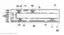
FIGS. 1A to 1L are cross-sectional views showing a manufacturing process according to an embodiment of the present invention. First, referring to FIG. 1A, a sacrifice layer 110, two third metal layers 120 disposed on two opposite surfaces of the sacrifice layer 110 and two first metal layers 130 disposed on the two third metal layers 120 are provided. Each third metal layer 120 is located between the sacrifice layer 110 and the corresponding first metal layer 130. In this embodiment, a first etching stopping layer 140 can be further formed on each first metal layer 130.
Next, referring to FIG. 1B, a first mask layer 150 is formed on each first etching stopping layer 140, wherein each first metal layer 130 is located between the corresponding third metal layer 120 and the corresponding first mask layer 150, and each first mask layer 150 exposes a part of the first metal layer 130.
Next, referring to FIG. 1C, a first patterned conductive layer 160 is formed on the part of the first metal layer 130 exposed by each first mask layer 150. The method of forming the first patterned conductive layers 160 can be electroplating. Then, referring to FIG. 1D, a second mask layer 170 is formed on each first mask layer 150, wherein each second mask layer 170 exposes a part of the corresponding first patterned conductive layer 160.
Next, referring to FIG. 1E, a plurality of first conductive blocks 180 are formed on the part of the first patterned conductive layer 160 exposed by each second mask layer 170. Then, referring to FIG. 1F, each second mask layer 170 and each first mask layer 150 are removed. Then, referring to FIG. 1G, each third metal layer 120 and the sacrifice layer 110 are removed to obtain two first conductive laminated structures 100a.
It should noted that each first conductive laminated structure 100a comprises a first metal layer 130, a first patterned conductive layer 160, a plurality of first conductive blocks 180 and a first etching stopping layer 140. Furthermore, in this embodiment, the method of removing the sacrifice layer 110 and each third metal layer 120 can be peeling each third metal layer 120 from the corresponding first metal layer 130.
Next, referring to FIG. 1H, a first dielectric layer 190 and a second conductive laminated structure 100b are provided. The first dielectric layer 190 has a first surface Si and a second surface S2 opposite to each. The second conductive laminated structure 100b comprises a second metal layer 130′, a second patterned conductive layer 160′ and a second etching stopping layer 140′ disposed between the second metal layer 130′ and the second patterned conductive layer 160′. It should be noted that the manufacturing method of the second conductive laminated structure 100b is similar to that of the first conductive laminated structure 100a and is not repeated herein.
Next, referring to FIG. 1I, the first conductive laminated structure 100a and the second conductive laminated structure 100b are laminated to the first dielectric layer 190 so that the first patterned conductive layer 160 and the first conductive blocks 180 are embedded in the first surface Si of the first dielectric layer 190 and the second patterned conductive layer 160′ is embedded in the second surface S2 of the first dielectric layer 190. The first patterned conductive layer 160 and the second patterned conductive layer 160′ are conducted via the first conductive blocks 180.
The first dielectric layer 190 has a plurality of first through holes H1 for containing the first conductive blocks 180. It should be noted that the first through holes H1 in the first dielectric layer 190 can be formed by embedding the conductive blocks 180 into the first dielectric layer 190 or can be formed in advance.
More particularly, a surface roughening on the first conductive blocks 180, the first patterned conductive layer 160 and the second patterned conductive layer 160′ can be conducted before embedding the first conductive laminated structure 100a and the second conductive laminated structure 100b to the first dielectric layer 190 to improve the bonding force of the first conductive blocks 180, the first patterned conductive layer 160 and the second patterned conductive layer 160′ to the first dielectric layer 190.
Next, referring to FIG. 1J, the first metal layer 130, the second metal layer 130′, the first etching stopping layer 140 and the second etching stopping layer 140′ are removed by etching. Specifically, the etchant applied on the first etching stopping layer 140 and the second etching stopping layer 140′ is different from that applied on the first metal layer 130, the second metal layer 130′, the first patterned conductive layer 160 and the second patterned conductive layer 160′. Therefore, over-etching to the first patterned conductive layer 160 and the second patterned conductive layer 160′ can be avoided when etching the first metal layer 130 and the second metal layer 130′.
Next, referring to FIG. 1K, a first solder mask layer L1 and a second solder mask layer L2 are respectively formed on the first patterned conductive layer 160 and the second patterned conductive layer 160′. The first solder mask layer L1 and the second solder mask layer L2 respectively expose a part of the first patterned conductive layer 160 and a part of the second patterned conductive layer 160′.
Next, referring to FIG. 1L, in this embodiment, a first anti-oxidation layer L3 and a second anti-oxidation layer L4 can be further formed on the part of the first patterned conductive layer 160 exposed by the first solder mask layer L1 and the part of the second patterned conductive layer 160′ exposed by the second solder mask layer L2, respectively. The method of forming the first anti-oxidation layer L3 and the second anti-oxidation layer L4 can be electroplating.
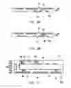
Referring to FIG. 1L, the embedded circuit substrate 100 of this embodiment comprises a first dielectric layer 190, a first patterned conductive layer 160, a second patterned conductive layer 160′, a plurality of first conductive blocks 180, a first solder mask layer L1, a second solder mask layer L2, a first anti-oxidation layer L3 and a second anti-oxidation layer L4.
The first dielectric layer 190 has a first surface S1 and a second surface S2 opposite to each other. The first patterned conductive layer 160 is disposed on the first surface S1 and embedded in the first dielectric layer 190. The second patterned conductive layer 160′ is disposed on the second surface S2 and embedded in the first dielectric layer 190. The first conductive blocks 180 are disposed in the first dielectric layer 190 for conducting the first patterned conductive layer 160 and the second patterned conductive layer 160′.
The first solder mask layer L1 and the second solder mask layer L2 are respectively disposed on the first patterned conductive layer 160 and the second patterned conductive layer 160′ for respectively exposing a part of the first patterned conductive layer 160 and a part of the second patterned conductive layer 160′. The first anti-oxidation layer L3 and the second anti-oxidation layer L4 are respectively disposed on the part of the first patterned conductive layer 160 exposed by the first solder mask layer L1 and the part of the second patterned conductive layer 160′ exposed by the second solder mask layer L2.
However, the aforementioned first conductive blocks 180 can further be formed by another method. FIGS. 2A and 2B are cross-sectional views showing a manufacturing process according to another embodiment of the present invention. Comparing with the manufacturing method of the embedded circuit substrate of FIG. 1I, the first conductive blocks 180 of this embodiment are not formed until the first conductive laminated structure 100a and the second conductive laminated structure 100b are laminated to the first dielectric layer 190.
Referring to FIG. 2A, after laminating the first conductive laminated structure 100a as shown in FIG. 1I but without the first conductive blocks 180 and the second conductive laminated structure 100b as shown in FIG. 1I to the first dielectric layer 190, and after removing the first metal layer 130, the second metal layer 130′, the first etching stopping layer 140 and the second etching stopping layer 140′, first through holes H1 are formed in the first dielectric layer 190 by a laser. Then, referring to FIG. 2B, the first conductive blocks 180 are formed in the first through holes H1 by electroplating or filling a conductive paste to obtain a structure similar to that of FIG. 1J, and the manufacturing process as shown in FIGS. 1K and 1L can therefore be performed sequentially.
FIG. 3 is a cross-sectional view showing an embedded circuit substrate according to further another embodiment of the present invention. Referring to FIG. 3, comparing with the embedded circuit substrate 100 of FIG. 1L, the embedded circuit substrate 100′ of this embodiment has a core structure 190′ instead of the first dielectric layer 190 of FIG. 1L. The core structure 190′ comprises a core dielectric layer 192, a third patterned conductive layer 194, a fourth patterned conductive layer 194′, a second dielectric layer 196, a third dielectric layer 196′ and at least one conductive via 198.
The core dielectric layer 192 has a third surface S3 and a fourth surface S4 opposite to each other. The third patterned conductive layer 194 is disposed on the third surface S3. The fourth patterned conductive layer 194′ is disposed on the fourth surface S4. The second dielectric layer 196 is disposed on the third patterned conductive layer 194, wherein the third patterned conductive layer 194 is located between the second dielectric layer 196 and the core dielectric layer 192, and the first conductive blocks 180 are located in the second dielectric layer 196 for connecting the first patterned conductive layer 160 and the third patterned conductive layer 194. The second dielectric layer 196 has a plurality of second through holes H2 for containing the first conductive blocks 180. The third dielectric layer 196′ is disposed on the fourth patterned conductive layer 194′, wherein the fourth patterned conductive layer 194′ is located between the third dielectric layer 196′ and the core dielectric layer 192. The conductive via 198 is located in the core dielectric layer 192 for conducting the third patterned conductive layer 194 and the fourth patterned conductive layer 194′.
Comparing with the embedded circuit substrate 100 of FIG. 1L, the embedded circuit substrate 100′ of this embodiment further comprises a plurality of second conductive blocks 180′ disposed on the second patterned conductive layer 160′ and located in the third dielectric layer 196′ for connecting the second patterned conductive layer 160′ and the fourth patterned conductive layer 194′. The third dielectric layer 196′ has a plurality of third through holes H3 for containing the second conductive blocks 180′. Furthermore, in this embodiment, the first patterned conductive layer 160 is embedded in the second dielectric layer 196 and the second patterned conductive layer 160′ is embedded in the third dielectric layer 196′. It should be noted that the manufacturing method of the embedded circuit substrate 100′ of this embodiment is similar to that of the embedded circuit substrate 100 of FIG. 1L and is not repeated herein.
In summary, the present invention embedding the patterned conductive layer and the conductive via in the dielectric layer at the same time by laminating such that the embedded circuit substrate has flat surface. Additionally, an embedded circuit substrate with a core dielectric layer in superior structural strength or another embedded circuit substrate without any core dielectric layer in lower thickness can be provided in the present invention according to different requirements.
It will be apparent to those skilled in the art that various modifications and variations can be made to the structure of the present invention without departing from the scope or spirit of the invention. In view of the foregoing, it is intended that the present invention cover modifications and variations of this invention provided they fall within the scope of the following claims and their equivalents.
Claims
What is claimed is:1. An embedded circuit substrate, comprising:
a core structure, having a first surface and a second surface opposite to each other;
a first patterned conductive layer, disposed on the first surface and embedded in the core structure;
a second patterned conductive layer, disposed on the second surface and embedded in the core structure; and
a plurality of conductive blocks, disposed in the core structure for conducting the first patterned conductive layer and the second patterned conductive layer.
2. The embedded circuit substrate according to claim 1, wherein the core structure comprises:
a first dielectric layer, wherein the conductive block is disposed in the first dielectric layer and connected between the first patterned conductive layer and the second patterned conductive layer.
3. The embedded circuit substrate according to claim 1, wherein the core structure comprises:
a core dielectric layer, having a third surface and a fourth surface opposite to each other;
a third patterned conductive layer, disposed on the third surface;
a fourth patterned conductive layer, disposed on the fourth surface;
a second dielectric layer, disposed on the third patterned conductive layer, wherein the third patterned conductive layer is located between the second dielectric layer and the core dielectric layer, and a part of the conductive blocks are located in the second dielectric layer to connect the first patterned conductive layer and the third patterned conductive layer;
a third dielectric layer, disposed on the fourth patterned conductive layer, wherein the fourth patterned conductive layer is located between the third dielectric layer and the core dielectric layer, and a part of the conductive blocks are located in the third dielectric layer to connect the second patterned conductive layer and the fourth patterned conductive layer; and
at least one conductive via, located in the core dielectric layer for conducting the third patterned conductive layer and the fourth patterned conductive layer.
4. The embedded circuit substrate according to claim 1, further comprising:
a first solder mask layer, disposed on the first patterned conductive layer to expose a part of the first patterned conductive layer, wherein the first patterned conductive layer is located between the first solder mask layer and the core structure.
5. The embedded circuit substrate according to claim 4, further comprising:
a first anti-oxidation layer, disposed on the part of the first patterned conductive layer exposed by the first solder mask layer.
6. The embedded circuit substrate according to claim 1, further comprising:
a second solder mask layer, disposed on the second patterned conductive layer to expose a part of the second patterned conductive layer, wherein the second patterned conductive layer is located between the second solder mask layer and the core structure.
7. The embedded circuit substrate according to claim 6, further comprising:
a second anti-oxidation layer, disposed on the part of the second patterned conductive layer exposed by the second solder mask layer.
8. A manufacturing method of embedded circuit substrate, comprising:
providing a core structure having a first surface and a second opposite to each other; and
providing a first conductive laminated structure, wherein the first conductive laminated structure comprises:
a first metal layer; and
a first patterned conductive layer, disposed on the first metal layer; and
providing a second conductive laminated structure, wherein the second conductive laminated structure comprises:
a second metal layer; and
a second patterned conductive layer, disposed on the second metal layer;
laminating the first conductive laminated structure and the second conductive laminated structure to the core structure, wherein the first patterned conductive layer is embedded in the first surface of the core structure, and the second patterned conductive layer is embedded in the second surface of the core structure;
forming a plurality of first conductive blocks in the core structure, wherein the first patterned conductive layer and the second patterned conductive layer are conducted via the first conductive blocks; and
removing the first metal layer and the second metal layer.
9. The manufacturing method of embedded circuit substrate according to claim 8, wherein the manufacturing method of the first conductive laminated structure comprises:
providing a sacrifice layer, a third metal layer disposed on the sacrifice layer and a first metal layer disposed on the third metal layer, wherein the third metal layer is located between the sacrifice layer and the first metal layer;
forming a first mask layer on the first metal layer, wherein the first metal layer is located between the third metal layer and the first mask layer, and the first mask layer exposes a part of the first metal layer;
forming a first patterned conductive layer on the part of the first metal layer exposed by the first mask layer; and
removing the first mask layer, the third metal layer and the sacrifice layer.
10. The manufacturing method of embedded circuit substrate according to claim 9, wherein the method of removing the first metal layer and the second metal layer comprises etching.
11. The manufacturing method of embedded circuit substrate according to claim 10, wherein the manufacturing method of the first conductive laminated structure further comprises:
forming a first etching stopping layer on the first metal layer before forming the first mask layer on the first metal layer.
12. The manufacturing method of embedded circuit substrate according to claim 9, wherein the core structure comprises a first dielectric layer.
13. The manufacturing method of embedded circuit substrate according to claim 12, wherein the first dielectric layer has a plurality of first through holes for containing the first conductive blocks.
14. The manufacturing method of embedded circuit substrate according to claim 13, wherein the method of forming the first conductive block comprises:
forming a second mask layer on the first mask layer before laminating the first conductive laminated structure and the second conductive laminated structure to the first dielectric layer, wherein the second mask layer exposes a part of the first patterned conductive layer;
forming the first conductive blocks on the part of the first patterned conductive layer exposed by the second mask layer;
removing the second mask layer before removing the first mask layer, the third metal layer and the sacrifice layer; and
embedding the first conductive blocks into the first dielectric layer when laminating the first conductive laminated structure and the second conductive laminated structure to the first dielectric layer.
15. The manufacturing method of embedded circuit substrate according to claim 13, wherein the method of forming the first conductive blocks comprises:
forming the first through holes in the first dielectric layer by a laser after removing the first metal layer and the second metal layer; and
forming the first conductive blocks in the first through holes by electroplating or filling a conductive paste.
16. The manufacturing method of embedded circuit substrate according to claim 8, further comprising:
forming a first solder mask layer on the first patterned conductive layer, wherein the first solder mask layer exposes a part of the first patterned conductive layer.
17. The manufacturing method of embedded circuit substrate according to claim 16, further comprising:
forming a first anti-oxidation layer on the part of the first patterned conductive layer exposed by the first solder mask layer.
18. The manufacturing method of embedded circuit substrate according to claim 8, further comprising:
forming a second solder mask layer on the second patterned conductive layer, wherein the second solder mask layer exposes a part of the second patterned conductive layer.
19. The manufacturing method of embedded circuit substrate according to claim 18, further comprising:
forming a second anti-oxidation layer on the part of the second patterned conductive layer exposed by the second solder mask layer.
20. The manufacturing method of embedded circuit substrate according to claim 8, further comprising:
performing a surface roughening to the first conductive block, the first patterned conductive layer and the second patterned conductive layer before laminating the first conductive laminated structure and the second conductive laminated structure to the core structure.
Images & Drawings included:


Sources:
- United States Patent and Trademark Office - verify current appl. status at the USPTO↗
Similar patent applications:
- » 20160284462
Coil-embedded integrated circuit substrate and method of manufacturing the same - » 20200075469
Method of manufacturing circuit carrier with embedded semiconductor substrate - » 20220039261
PRINTED CIRCUIT BOARD, ELECTRONIC COMPONENT-EMBEDDED SUBSTRATE, AND MANUFACTURING METHOD THEREOF - » 20120152886
METHOD OF MANUFACTURING SUBSTRATE FOR CAPACITOR-EMBEDDED PRINTED CIRCUIT BOARD AND CAPACITOR-EMBEDDED PRINTED CIRCUIT BOARD - » 20070227763
Coreless thin substrate with embedded circuits in dielectric layers and method for manufacturing the same - » 20150001705
Integrated circuit packaging system with embedded pad on layered substrate and method of manufacture thereof - » 20170162495
Integrated circuit packaging system with embedded pad on layered substrate and method of manufacture thereof - » 20130075922
Integrated circuit packaging system with a substrate embedded dummy-die paddle and method of manufacture thereof - » 20090244864
Substrate for capacitor-embedded printed circuit board, capacitor-embedded printed circuit board and manufacturing method thereof
Recent applications in this class:
- » 20210360798 2021-11-18
Printed Circuit Board and Vehicle Having the Same - » 20210127503 2021-04-29
Ultra-thin copper foil, ultra-thin copper foil with carrier, and method for manufacturing printed wiring board - » 20210092854 2021-03-25
Methods for laser welding layers of circuitry pattern in the reel-to-reel fabrication of flexible printed circuits - » 20130062106 2013-03-14
Printed Circuit Board and Method of Manufacturing the Same - » 20120210576 2012-08-23
PRINTED CIRCUIT BOARD AND METHOD OF MANUFACTURING THE SAME - » 20110005824 2011-01-13
PRINTED CIRCUIT BOARD AND METHOD OF MANUFACTURING THE SAME
Recent applications for this Assignee:
- » 20250294670 2025-09-18
ELECTRONIC DEVICE - » 20250293221 2025-09-18
ELECTRONIC DEVICE - » 20250285950 2025-09-11
SEMICONDUCTOR DEVICE PACKAGE - » 20250282612 2025-09-11
PACKAGE STRUCTURE - » 20250273638 2025-08-28
SEMICONDUCTOR DEVICE PACKAGE INCLUDING STRESS BUFFERING LAYER - » 20250273531 2025-08-28
PACKAGE STRUCTURE - » 20250271555 2025-08-28
OPTOELECTRONIC STRUCTURE - » 20250266313 2025-08-21
SEMICONDUCTOR DEVICE PACKAGE AND METHOD OF MANUFACTURING THE SAME - » 20250260153 2025-08-14
ELECTRONIC DEVICE - » 20250259978 2025-08-14
SEMICONDUCTOR PACKAGE DEVICE AND METHOD OF MANUFACTURING THE SAME