Method of manufacturing wafer level package including coating and removing resin over the dicing lines
US20100159646A1
2010-06-24
12/453,273
2009-05-05
✅ Patent granted
US 7,947,530 B2
2011-05-24
-
-
William M. Brewster
2029-10-08
Abstract:
The present invention relates to a method of manufacturing a wafer level package including the steps of: preparing a substrate wafer including a plurality of pads formed on a bottom surface, a plurality of chips positioned on a top surface, and dicing lines for dividing the chips; forming external connection units on the pads; coating resin on the dicing lines by positioning masks on the substrate wafer to expose only the dicing lines; removing the masks; encapsulating the chips positioned between the resin by coating the chips with encapsulant; removing the resin coated on the dicing lines; and cutting a wafer level package along the dicing lines exposed by removing the resin into units.
Inventors:
- Seung Wook Park 289 🇰🇷 Seoul, South Korea
- Young Do KWEON 72 🇰🇷 Seoul, South Korea
- Seon Hee Moon 12 🇰🇷 Seoul, South Korea
- Jin Gu Kim 24 🇰🇷 Suwon-si, South Korea
- Hyung Jin Jeon 11 🇰🇷 Gunpo-si, South Korea
- Hee Kon Lee 4 🇰🇷 Hwaseong-si, South Korea
Assignee:
- SAMSUNG ELECTRO-MECHANICS CO., LTD. 3,010 🇰🇷 Suwon, South Korea
Interested in similar patents?
Get notified when new applications in this technology area are published.
Classification:
H01L21/561 » CPC main
Processes or apparatus adapted for the manufacture or treatment of semiconductor or solid state devices or of parts thereof; Manufacture or treatment of semiconductor devices or of parts thereof the devices having at least one potential-jump barrier or surface barrier, e.g. PN junction, depletion layer or carrier concentration layer; Assembly of semiconductor devices using processes or apparatus not provided for in a single one of the subgroups - , e.g. sealing of a cap to a base of a container; Encapsulations, e.g. encapsulation layers, coatings Batch processing
H01L23/24 » CPC further
Details of semiconductor or other solid state devices; Fillings or auxiliary members in containers or encapsulations , e.g. centering rings; Fillings characterised by the material, its physical or chemical properties, or its arrangement within the complete device solid or gel at the normal operating temperature of the device
H01L23/3121 » CPC further
Details of semiconductor or other solid state devices; Encapsulations, e.g. encapsulating layers, coatings, e.g. for protection characterised by the arrangement or shape the device being completely enclosed a substrate forming part of the encapsulation
H01L24/94 » CPC further
Arrangements for connecting or disconnecting semiconductor or solid-state bodies; Methods or apparatus related thereto; Batch processes at wafer-level, i.e. with connecting carried out on a wafer comprising a plurality of undiced individual devices
H01L2924/09701 » CPC further
Indexing scheme for arrangements or methods for connecting or disconnecting semiconductor or solid-state bodies as covered by with a principal constituent of the material being a combination of two or more materials provided in the groups - ; Glass-ceramics, e.g. devitrified glass Low temperature co-fired ceramic [LTCC]
H01L2924/3511 » CPC further
Indexing scheme for arrangements or methods for connecting or disconnecting semiconductor or solid-state bodies as covered by; Technical effects; Mechanical effects; Thermal stress Warping
H01L2924/181 » CPC further
Indexing scheme for arrangements or methods for connecting or disconnecting semiconductor or solid-state bodies as covered by; Details of package parts other than the semiconductor or other solid state devices to be connected Encapsulation
H01L2924/00 » CPC further
Indexing scheme for arrangements or methods for connecting or disconnecting semiconductor or solid-state bodies as covered by
H01L21/78 IPC
Processes or apparatus adapted for the manufacture or treatment of semiconductor or solid state devices or of parts thereof; Manufacture or treatment of devices consisting of a plurality of solid state components formed in or on a common substrate or of parts thereof; Manufacture of integrated circuit devices or of parts thereof; Manufacture or treatment of devices consisting of a plurality of solid state components or integrated circuits formed in, or on, a common substrate with subsequent division of the substrate into plural individual devices
H01L21/44 IPC
Processes or apparatus adapted for the manufacture or treatment of semiconductor or solid state devices or of parts thereof; Manufacture or treatment of semiconductor devices or of parts thereof the devices having at least one potential-jump barrier or surface barrier, e.g. PN junction, depletion layer or carrier concentration layer the devices having semiconductor bodies not provided for in groups, , , and with or without impurities, e.g. doping materials Manufacture of electrodes on semiconductor bodies using processes or apparatus not provided for in groups -
H01L21/48 IPC
Processes or apparatus adapted for the manufacture or treatment of semiconductor or solid state devices or of parts thereof; Manufacture or treatment of semiconductor devices or of parts thereof the devices having at least one potential-jump barrier or surface barrier, e.g. PN junction, depletion layer or carrier concentration layer Manufacture or treatment of parts, e.g. containers, prior to assembly of the devices, using processes not provided for in a single one of the subgroups -
H01L21/50 IPC
Processes or apparatus adapted for the manufacture or treatment of semiconductor or solid state devices or of parts thereof; Manufacture or treatment of semiconductor devices or of parts thereof the devices having at least one potential-jump barrier or surface barrier, e.g. PN junction, depletion layer or carrier concentration layer Assembly of semiconductor devices using processes or apparatus not provided for in a single one of the subgroups - , e.g. sealing of a cap to a base of a container
Description
CROSS-REFERENCE TO RELATED APPLICATIONS
This application claims the benefit of Korean Patent Application No. 10-2008-0130219 filed with the Korea Intellectual Property Office on Dec. 19, 2008, the disclosure of which is incorporated herein by reference.
BACKGROUND OF THE INVENTION
1. Field of the Invention
The present invention relates to a method of manufacturing a wafer level package; and, more particularly, to a method of manufacturing a wafer level package to coat resin on a dicing line formed on a substrate wafer.
2. Description of the Related Art
A conventional package is manufactured by cutting a wafer having a plurality of chips along dicing lines to be divided into individual chips and then performing a packaging process for each of the individual chips.
However, because the packaging process includes a lot of unit processes, e.g., chip attaching, wire bonding, molding, trimming/forming or the like, a conventional method of manufacturing the package to perform the packaging process by each of the chips has a disadvantage of needing a very long time for packaging all of the chips when considering the number of the chips obtained from one wafer.
Therefore, recently, there has been suggested a wafer level package method of manufacturing an individual package by firstly performing the packaging process in a wafer level and then cutting a wafer level package along dicing lines of a wafer.
In the wafer level package, it is general that after a molding process is performed on the wafer provided with a chip or the like by using molding resin such as EMC(Epoxy Mold Compound), the surface of the molding resin is formed to be flat. However, if the molding resin has the flat surface, the CTE(Coefficient of Thermal Expansion) of the molding resin is more than double to ten times the CTE of the wafer and so the molding resin may be considerably contracted due to heat generated in the molding process, which causes a warpage phenomenon where the wafer is rolled and makes the dicing lines unseen.
SUMMARY OF THE INVENTION
The present invention has been invented in order to overcome the above-described problems and it is, therefore, an object of the present invention to provide a method of manufacturing a wafer level package capable of preventing a warpage phenomenon where a wafer is rolled in an encapsulation process by coating resin on dicing lines formed on a substrate wafer and of smoothly performing dicing work by cutting a wafer level package along dicing lines exposed by removing the resin.
In accordance with one aspect of the present invention to achieve the object, there is provided a method of manufacturing a wafer level package including the steps of: preparing a substrate wafer including a plurality of pads formed on a bottom surface, a plurality of chips positioned on a top surface, and dicing lines for dividing the chips; forming external connection units on the pads; coating resin on the dicing lines by positioning masks on the substrate wafer to expose only the dicing lines; removing the masks; encapsulating the chips positioned between the resin by coating the chips with encapsulant; removing the resin coated on the dicing lines; and cutting a wafer level package along the dicing lines exposed by removing the resin into units.
Further, the resin can be formed of any one of transparent, translucent, or opaque photocurable, thermosetting, and thermoplastic resin in the step of coating the resin on the dicing lines.
Further, the method further includes a step of: curing the resin after the step of coating the resin on the dicing lines.
Further, the encapsulant can be formed of liquid resin or solid epoxy mold compound in the step of encapsulating the chips on the substrate with the encapsulant.
Further, the encapsulant can be coated by any one of printing, dispensing, dipping, spin coating, compression molding, and transfer molding in the step of encapsulating the chips on the substrate with the encapsulant.
Further, the resin can be removed by a wet method or a plasma method in the step of removing the resin coated on the dicing lines.
In accordance with another aspect of the present invention to achieve the object, there is provided a method of manufacturing a wafer level package including the steps of: preparing a substrate wafer including a plurality of pads formed on a bottom surface, a plurality of chips positioned on a top surface, and dicing lines for dividing the chips; forming external connection units on the pads; coating resin on the dicing lines by positioning masks on the substrate wafer to expose only the dicing lines; removing the masks; encapsulating the chips positioned between the resin by coating the chips with encapsulant; and cutting a wafer level package along the dicing lines coated with the resin into units.
Further, the resin can be formed of any one of transparent photocurable, thermosetting, and thermoplastic resin in the step of coating the resin on the dicing lines.
BRIEF DESCRIPTION OF THE DRAWINGS
These and/or other aspects and advantages of the present general inventive concept will become apparent and more readily appreciated from the following description of the embodiments, taken in conjunction with the accompanying drawings of which:
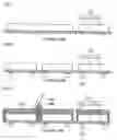
FIGS. 1 to 8 are cross-sectional views sequentially illustrating a method of manufacturing a wafer level package in accordance with an embodiment of the present invention; and
FIG. 9 is a cross-sectional view illustrating a method of manufacturing a wafer level package in accordance with another embodiment of the present invention.
DETAILED DESCRIPTION OF THE PREFERABLE EMBODIMENTS
Hereinafter, a matter regarding to an operation effect including a technical configuration for a method of manufacturing a wafer level package in accordance with the present invention will be appreciated clearly through the following detailed description with reference to the accompanying drawings illustrating preferable embodiments of the present invention.
Methods of manufacturing wafer level packages in accordance with embodiments of the present invention will be described in detail with reference to FIGS. 1 to 9.
FIGS. 1 to 8 are cross-sectional views sequentially illustrating a method of manufacturing a wafer level package in accordance with an embodiment of the present invention and FIG. 9 is a cross-sectional view illustrating a method of manufacturing a wafer level package in accordance with another embodiment of the present invention.
At first, as shown in FIG. 1, there is prepared a substrate wafer 110 including a plurality of pads 113 formed on a bottom surface, a plurality of chips 115 positioned on a top surface, and dicing lines for dividing the chips 115.
At this time, the dicing lines are formed at equal intervals in a row direction and a column direction in which the chips 115 are positioned and can be processed by any one of a sanding process where the surface of the substrate wafer 110 is slightly cut or carved, an etching process as a surface processing method applying erosive action of chemical agents or an ultrasound process as another surface processing method using ultrasound vibration.
And, inside the substrate wafer 110, there can be further formed via holes(not shown in the drawings) for electrical connection between the chips 115 and external connection units 120 to be formed on the pads 113 later.
Herein, material of the substrate wafer 110 as a substrate used in a semiconductor process can be silicon, ceramic, glass, polymer, and so on.
Then, as illustrated in FIG. 2, the external connection units 120 are formed on the pads 113 of the substrate wafer 110. The external connection units 120 can be solder balls which are electrically connected through the medium of the pads 113. At this time, the external connection units 120 can be formed of solder bumps with another shape other than the solder balls.
Then, as shown in FIG. 3, resin 140a is coated on the dicing lines after positioning masks 130 on the substrate wafer 110 to expose only the dicing lines. At this time, the resin 140a coated on the surfaces of the masks 130 is pushed in the dicing lines with a squeeze 142 to be uniformly coated. And, any one of a mask patterned by photoresist or a screen printing mask can be used as the mask. Further, it is preferable that the resin 140a and 140b is formed of any one of transparent, translucent, or opaque photocurable, thermosetting, and thermoplastic resin.
Then, as illustrated in FIGS. 4 and 5, after curing the resin 140a for a predetermined time, the masks 130 are removed. At this time, the resin 140a is cured by irradiating ultraviolet rays through a UV curing system or applying heat at more than a predetermined temperature. Therefore, the resin 140a is firmly fixed between the chips 115 positioned on the substrate wafer 110, i.e., on the dicing lines for dividing the chips 115.
Then, as shown in FIG. 6, the chips 115 positioned between the resin 140a are encapsulated by being coated with encapsulant 150 in order to finish a wafer level package. The encasulant 150 can be made of liquid resin, solid epoxy mold compound, or the like and the encapsulant can be coated by any one of printing, dispensing, dipping, spin coating, compression molding, and transfer molding.
At this time, the resin 140a formed on the dicing lines for dividing the chips 115 narrows a region where stress generated due to a CTE(Coefficient of Thermal Expansion) difference between the encapsulant 150 and the substrate wafer 110 is transmitted in order to reduce the stress so that power contracting the substrate wafer 110 in an encapsulation process can be distributed. Therefore, it is possible to improve a warpage phenomenon of the substrate wafer 110.
Then, as shown in FIG. 7, the resin 140a is removed. At this time, the resin 140a can be removed by a wet method using chemical agents such as permanganate or a plasma method using plasma as an aggregate of particles consisting of ion-nuclei and free electrons, which is formed by continuing to apply heat to material of a gaseous state in order to increase a temperature.
However, in case that the resin 140b is coated on the dicing lines by using any one of the transparent photocurable, thermosetting, and thermoplastic resin in a step of coating the resin on the dicing lines, dicing work can be performed along the dicing lines coated with the resins 140 without removing the resin 140b as shown in FIG. 9. In this case, a process before the step of coating the resin 140b on the dicing lines is performed similarly, while a step of removing the resins 140b is omitted, thereby enhancing workability and productivity.
Then, a s shown in FIG. 8, the wafer level package is cut along the dicing lines exposed by removing the resins 140a into units. Accordingly, dicing work can be smoothly accomplished by cutting it along the exposed dicing lines.
And, the dicing work of the wafer level package is performed with a dicing blade(not shown in the drawings), wherein the dicing blade is a semiconductor wafer processing device capable of exactly cutting a subject at a high speed without attaching shavings to a cutting surface. As described above, if the wafer level package is diced along the exposed dicing lines, a region to be diced by the dicing blade is reduced in order to reduce pressure applied to the dicing blade, thereby increasing durability and wear resistance of the dicing blade.
As described above, the method of manufacturing the wafer level package in accordance with the present invention can narrow the region where the stress generated due to the CTE difference between the encapsulant 150 and the substrate wafer 110 is transmitted in the encapsulation process in order to reduce the stress by coating the resin 140a and 140b on the dicing lines formed on the substrate wafer 110, so that the power by which the substrate wafer 110 is contracted can be distributed in order to improve the warpage phenomenon of the substrate wafer 110.
Further, thereafter, in case that the resin 140a is removed, the dicing work can be smoothly accomplished by cutting it along the exposed dicing lines, thereby remarkably enhancing quality and yield of the wafer level package. Consequently, the workability and the productivity of the wafer level package can be enhanced.
As described above, although the preferable embodiments of the present invention have been shown and described, it will be appreciated by those skilled in the art that substitutions, modifications and changes may be made in this embodiment without departing from the principles and spirit of the general inventive concept, the scope of which is defined in the appended claims and their equivalents.
Claims
1. A method of manufacturing a wafer level package comprising:
preparing a substrate wafer including a plurality of pads formed on a bottom surface, a plurality of chips positioned on a top surface and dicing lines for dividing the chips;
forming external connection units on the pads;
coating resin on the dicing lines by positioning masks on the substrate wafer to expose only the dicing lines;
removing the masks;
encapsulating the chips positioned between the resin by coating the chips with encapsulant;
removing the resin coated on the dicing lines; and
cutting a wafer level package along the dicing lines exposed by removing the resin into units.
2. The method of claim 1, wherein the resin is formed of any one of transparent, translucent, or opaque photocurable, thermosetting, and thermoplastic resin in the coating the resin on the dicing lines.
3. The method of claim 1, further comprising: curing the resin after the coating the resin on the dicing lines.
4. The method of claim 1, wherein the encapsulant is formed of liquid resin or solid epoxy mold compound in the encapsulating the chips on the substrate with the encapsulant.
5. The method of claim 1, wherein the encapsulant is coated by any one of printing, dispensing, dipping, spin coating, compression molding, and transfer molding in the encapsulating the chips on the substrate with the encapsulant.
6. The method of claim 1, wherein the resin is removed by a wet method or a plasma method in the removing the resin coated on the dicing lines.
7. A method of manufacturing a wafer level package comprising:
preparing a substrate wafer including a plurality of pads formed on a bottom surface, a plurality of chips positioned on a top surface, and dicing lines for dividing the chips;
forming external connection units on the pads;
coating resin on the dicing lines by positioning masks on the substrate wafer to expose only the dicing lines;
removing the masks;
encapsulating the chips positioned between the resin by coating the chips with encapsulant; and
cutting a wafer level package along the dicing lines coated with the resin into units.
8. The method of claim 7, wherein the resin is formed of any one of transparent photocurable, thermosetting, and thermoplastic resin in the coating the resin on the dicing lines.
Images & Drawings included:


Sources:
- United States Patent and Trademark Office - verify current appl. status at the USPTO↗
Recent applications in this class:
- » 20250239463 2025-07-24
SEMICONDUCTOR DEVICE AND METHOD FOR FABRICATING THE SAME - » 20250226238 2025-07-10
METHOD FOR MANUFACTURING SEMICONDUCTOR DEVICE AND SEMICONDUCTOR DEVICE - » 20250218799 2025-07-03
PHOTONIC INTEGRATED PACKAGE AND METHOD FORMING SAME - » 20250218798 2025-07-03
METHODS AND DEVICES FOR PROCESSING SINGULATED SUBSTRATES - » 20250210376 2025-06-26
METHOD OF PACKAGING SEMICONDUCTOR DIES - » 20250201583 2025-06-19
MANUFACTURING METHOD OF SEMICONDUCTOR PACKAGE - » 20250183057 2025-06-05
CARRIER FILM DISPOSED ON A MOTHER SUBSTRATE AND METHOD OF MANUFACTURING A SEMICONDUCTOR PACKAGE - » 20250149347 2025-05-08
METHOD FOR FABRICATING SEMICONDUCTOR PACKAGING STRUCTURE AND SEMICONDUCTOR PACKAGING STRUCTURE FABRICATED USING THE SAME - » 20250118574 2025-04-10
METHOD OF MANUFACTURING SEMICONDUCTOR PACKAGES - » 20250054776 2025-02-13
SEMICONDUCTOR PACKAGES WITH PATTERNS OF DIE-SPECIFIC INFORMATION
Recent applications for this Assignee:
- » 20170293104 2017-10-12
Lens module - » 20160242284 2016-08-18
PRINTED CIRCUIT BOARD HAVING METAL BUMPS - » 20160148750 2016-05-26
COIL COMPONENT - » 20160126745 2016-05-05
Non-contact type power transmitting apparatus, non-contact type power receiving apparatus, and non-contact type power transceiving apparatus - » 20160088201 2016-03-24
CAMERA MODULE - » 20160037624 2016-02-04
FLEXIBLE PRINTED CIRCUIT BOARD AND MANUFACTURING METHOD THEREOF - » 20150373842 2015-12-24
SUBSTRATE STRIP, SUBSTRATE PANEL, AND MANUFACTURING METHOD OF SUBSTRATE STRIP - » 20150364992 2015-12-17
Charge pump system and charge pump protection circuit - » 20150364585 2015-12-17
POWER SEMICONDUCTOR DEVICE - » 20150355777 2015-12-10
Integration circuit, touch interaction sensing apparatus, and touchscreen apparatus