CHIP PACKAGE WITH STACKED INDUCTORS
US20100164058A1
2010-07-01
12/429,870
2009-04-24
Abstract:
A semiconductor chip package with inductors includes a substrate, a semiconductor chip, an inductor and an insulator cover. The substrate has an active surface with a patterned circuit thereon. The inductor disposes on the active surface of the substrate. The semiconductor chip stacks over the inductor and electrically interconnects with the patterned circuit of the substrate and the inductor. The insulator cover encapsulates the inductor and the chip.
Interested in similar patents?
Get notified when new applications in this technology area are published.
Classification:
H01L23/3121 » CPC main
Details of semiconductor or other solid state devices; Encapsulations, e.g. encapsulating layers, coatings, e.g. for protection characterised by the arrangement or shape the device being completely enclosed a substrate forming part of the encapsulation
H01L23/645 » CPC further
Details of semiconductor or other solid state devices; Structural electrical arrangements for semiconductor devices not otherwise provided for, e.g. in combination with batteries; Impedance arrangements Inductive arrangements
H01L25/16 » CPC further
Assemblies consisting of a plurality of individual semiconductor or other solid state devices ; Multistep manufacturing processes thereof the devices being of types provided for in two or more different main groups of - , e.g. forming hybrid circuits
H01L24/48 » CPC further
Arrangements for connecting or disconnecting semiconductor or solid-state bodies; Methods or apparatus related thereto; Means for bonding being attached to, or being formed on, the surface to be connected, e.g. chip-to-package, die-attach, "first-level" interconnects; Manufacturing methods related thereto; Wire connectors; Manufacturing methods related thereto; Structure, shape, material or disposition of the wire connectors after the connecting process of an individual wire connector
H01L24/73 » CPC further
Arrangements for connecting or disconnecting semiconductor or solid-state bodies; Methods or apparatus related thereto Means for bonding being of different types provided for in two or more of groups , , , , , , ,
H01L2924/19103 » CPC further
Indexing scheme for arrangements or methods for connecting or disconnecting semiconductor or solid-state bodies as covered by; Details of hybrid assemblies other than the semiconductor or other solid state devices to be connected; Disposition of discrete passive components in a stacked assembly with the semiconductor or solid state device interposed between the semiconductor or solid-state device and the die mounting substrate, i.e. chip-on-passive
H01L2224/73265 » CPC further
Indexing scheme for arrangements for connecting or disconnecting semiconductor or solid-state bodies and methods related thereto as covered by; Means for bonding being of different types provided for in two or more of groups; Location after the connecting process on different surfaces Layer and wire connectors
H01L2924/181 » CPC further
Indexing scheme for arrangements or methods for connecting or disconnecting semiconductor or solid-state bodies as covered by; Details of package parts other than the semiconductor or other solid state devices to be connected Encapsulation
H01L2924/00012 » CPC further
Indexing scheme for arrangements or methods for connecting or disconnecting semiconductor or solid-state bodies as covered by; Technical content checked by a classifier Relevant to the scope of the group, the symbol of which is combined with the symbol of this group
H01L2224/45099 » CPC further
Indexing scheme for arrangements for connecting or disconnecting semiconductor or solid-state bodies and methods related thereto as covered by; Means for bonding being attached to, or being formed on, the surface to be connected, e.g. chip-to-package, die-attach, "first-level" interconnects; Manufacturing methods related thereto; Wire connectors; Manufacturing methods related thereto; Structure, shape, material or disposition of the wire connectors prior to the connecting process of an individual wire connector; Core members of the connector Material
H01L2924/00014 » CPC further
Indexing scheme for arrangements or methods for connecting or disconnecting semiconductor or solid-state bodies as covered by; Technical content checked by a classifier the subject-matter covered by the group, the symbol of which is combined with the symbol of this group, being disclosed without further technical details
H01L2924/207 » CPC further
Indexing scheme for arrangements or methods for connecting or disconnecting semiconductor or solid-state bodies as covered by; Parameters Diameter ranges
H01L27/04 IPC
Devices consisting of a plurality of semiconductor or other solid-state components formed in or on a common substrate including semiconductor components specially adapted for rectifying, oscillating, amplifying or switching and having at least one potential-jump barrier or surface barrier; including integrated passive circuit elements with at least one potential-jump barrier or surface barrier the substrate being a semiconductor body
Description
BACKGROUND OF THE INVENTION
1. Field of the Invention
The present invention relates to semiconductor chip packages, and more particularly, to semiconductor chip packages with stacked inductors.
2. Description of the Related Art
To satisfy the demand for a small size semiconductor chip with inductors, U.S. Pat. No. 6,512,285 discloses a structure for integrating an inductor on a package substrate of a chip. From the disclosure thereof, such a structure indeed reduces the size of the prior art chip. But as shown in FIG. 1 thereof, in the structure, an inductor 108 and a chip 102 are situated on top surface 104 of substrate 106. In other words, inductor 108 and chip 102 are arranged on the same plane. The result is that the structure needs a large size substrate to accommodate both inductor and chip so that the size of the whole chip package can not be substantially reduced.
The primary objective of the invention therefore is to reduce the size of a chip package with inductors.
Another objective of the invention is to provide a chip package having a small size inductor stacked thereon.
SUMMARY OF THE INVENTION
Thus, a chip package according to the invention comprises a substrate, a semiconductor chip, an inductor and an insulator cover. The substrate has an active surface with a patterned circuit thereon. The inductor attaches on the active surface of the substrate. The semiconductor chip stacks over the inductor and electrically interconnects with the patterned circuit of the substrate and the inductor. The insulator cover encapsulates the inductor and the chip.
BRIEF DESCRIPTION OF THE DRAWINGS
The above and other objectives, advantages and features of the invention will become clearer from the following description of the preferred embodiment with reference to the attached drawings, wherein:
FIG. 1 is a sectional view of a first embodiment of the invention;
FIG. 2 is a sectional view of a second embodiment of the invention;
FIG. 3 is a partly exploded view of the chip package as shown in FIG. 2;
FIG. 4 is a sectional view of a third embodiment of the invention; and
FIG. 5 is a perspective view of an inductor of the chip package as shown in FIG. 4.
DETAILED DESCRIPTION OF PREFERRED EMBODIMENTS
Referring firstly to FIG. 1, a chip package 10 according to one embodiment of the invention includes a substrate 12, an inductor 14, a semiconductor chip 1 6 and an insulator cover 18.
Substrate 12 is a conventional substrate for chip packaging, such as PCB. It has an active surface 20 with a patterned circuit.
Inductor 14 includes a core 22 made of a material with high permeability, such as ferrite, and a coil 24 encircling thereon. In this embodiment, a first insulator layer (not shown in the drawing) disposes between inductor 14 and active surface 20 of substrate 12. Inductor 14 is electrically interconnected to the patterned circuit of active surface 20 of substrate 12 by conductive wires 26.
Semiconductor chip 16 is stacked over inductor 14. A second insulator layer (not shown in the drawing) disposes between chip 16 and inductor 14. Chip 16 is electrically interconnected to the patterned circuit of active surface 20 of substrate 12 by conductive wires 28.
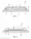
Referring now to FIGS. 2 and 3, chip package 30 according to another embodiment of the invention includes a semiconductor chip 32 and inductor 34, which are orderly stacked over active surface 40 of substrate 38. In this embodiment, inductor 34, as shown in FIG. 3, includes a core 42 made of ferrite, an upper winding 44 and a lower winding 46. Upper winding 44 has a plurality of first conductive segments 442 disposed on upper surface 48 of core 42 by any prior art method, such as embedded or coated processing. Lower winding 46 also has a plurality of second conductive segments 462 disposed on active surface 40 of substrate 38 by any prior art method, such as coating or printing processing. Upper winding 44 and lower winding 46 are electrically interconnected by bonding wires 50 so as to form a complete coil of inductor 34.
Referring lastly to FIGS. 4 and 5, chip package 60 is similar to chip packages 10 and 30 wherein chip 62 and inductor 64 are orderly stacked on active surface 70 of substrate 68 and an insulator layer 66 is disposed between chip 62 and inductor 64. The difference among them is that, in this embodiment, inductor 64 includes a base 72 made of insulating materials, a lower winding 74 is disposed on upper surface 76 of base 72, a core 78 made of ferrite is stacked over lower winding 74, an upper winding 80 is disposed on upper surface 82 of core 78, and upper winding 80 and lower winding 74 are electrically interconnected by bonding wires 84.
It is manifest from the above description of the invention that the chip and the inductor are orderly stacked over the substrate so that the size of the whole chip package is substantially reduced.
It should be understood that the invention is not limited to the particular embodiments described herein, but is capable of many rearrangements, modifications, and substitutions without departing from the scope of the invention.
Claims
What is claimed is:1. A chip package, comprising:
a substrate having an active surface with a patterned circuit thereon;
an inductor attached on said active surface of said substrate;
a semiconductor chip stacked over said inductor and electrically interconnected with said patterned circuit and said inductor; and
an insulator cover encapsulating said inductor and said chip.
2. The chip package of claim 1, wherein said inductor includes a core made of a material with high permeability, and a coil encircling on said core.
3. The chip package of claim 1, further comprising a first insulator layer disposed between said inductor and said substrate.
4. The chip package of claim 1, further comprising a second insulator layer disposed between said inductor and said chip.
5. The chip package of claim 1, wherein said inductor includes:
a base having an upper surface;
a plurality of first conductive segments separately disposed on said upper surface of said base;
a core made of a material with high permeability stacked over said first conductive segments; and
a plurality of second conductive segments separately disposed on said core, said second conductive segments electrically interconnecting with said first conductive segments to form an inductor coil.
6. A chip package, comprising:
a substrate having an active surface with a patterned circuit thereon;
a semiconductor chip attached on said active surface of said substrate and electrically interconnected with said patterned circuit thereof;
an inductor disposed between said substrate and said chip, said inductor includes:
a lower winding disposed on said active surface of said substrate;
a core made of a material with high permeability stacked over said lower winding;
an upper winding disposed on said core; and
said lower winding electrically interconnected with said upper winding to form an inductor coil; and
an insulator cover encapsulating said inductor and said chip.
7. The chip package of claim 6, wherein said lower winding includes a plurality of first conductive segments separately disposed on said active surface of said substrate.
8. The chip package of claim 6, wherein said upper winding includes a plurality of second conductive segments separately disposed on said core.
9. The chip package of claim 8, wherein said first conductive segments and said second conductive segments are electrically interconnected by a plurality of bonding wires.
Images & Drawings included:


Sources:
- United States Patent and Trademark Office - verify current appl. status at the USPTO↗
Recent applications in this class:
- » 20250174507 2025-05-29
SEMICONDUCTOR DEVICE HAVING EMBEDDED DIE AND METHOD THEREFOR - » 20250149395 2025-05-08
POWER MODULES HAVING ENCAPSULATION STRESS AND STRAIN MITIGATING CONFIGURATIONS - » 20250140622 2025-05-01
METHOD OF FIXING PROTECTIVE MEMBER - » 20250140621 2025-05-01
Stacked Power Converter Assembly - » 20250132213 2025-04-24
SEMICONDUCTOR PACKAGING STRUCTURE - » 20250125207 2025-04-17
SEMICONDUCTOR MODULE AND MANUFACTURING METHOD THEREFOR - » 20250054825 2025-02-13
SEMICONDUCTOR PACKAGE AND SEMICONDUCTOR ASSEMBLY INCLUDING THE SAME - » 20250046664 2025-02-06
SEMICONDUCTOR DEVICE - » 20250046663 2025-02-06
SEMICONDUCTOR PACKAGE AND METHOD OF MANUFACTURING THE SEMICONDUCTOR PACKAGE - » 20250046662 2025-02-06
PACKAGING STRUCTURE, ELECTRONIC PACKAGE, AND METHODS FOR MANUFACTURING THE SAME