Photoconductors for mid-/far-IR detection
US20100187530A1
2010-07-29
12/359,513
2009-01-26
✅ Patent granted
US 8,115,203 B2
2012-02-14
-
-
Jarrett Stark
2029-01-26
Abstract:
An infrared photodiode structure is provided. The infrared photodiode structure includes a doped semiconductor layer having ions of certain conductivity. An active photodetecting region is positioned on the doped semiconductor layer for detecting an infrared light signal. The active photodetecting region includes one or more amorphous semiconductor materials so as to allow for high signal-to-noise ratio being achieved by invoking carrier hopping and band conduction, under dark and illuminated conditions.
Inventors:
- Lionel C. Kimerling 75 🇺🇸 Concord, MA, United States
- Juejun Hu 9 🇺🇸 Cambridge, MA, United States
- Anuradha M. Agarwal 25 🇺🇸 Weston, MA, United States
- Ning-Ning Feng 5 🇺🇸 Somerville, MA, United States
- Anuradha Agarwal 2 🇺🇸 Weston, MA, United States
Assignee:
- MASSACHUSETTS INSTITUTE OF TECHNOLOGY 7,186 🇺🇸 Cambridge, MA, United States
Interested in similar patents?
Get notified when new applications in this technology area are published.
Classification:
H01L31/109 » CPC main
Semiconductor devices sensitive to infra-red radiation, light, electromagnetic radiation of shorter wavelength or corpuscular radiation and specially adapted either for the conversion of the energy of such radiation into electrical energy or for the control of electrical energy by such radiation; Processes or apparatus specially adapted for the manufacture or treatment thereof or of parts thereof; Details thereof in which radiation controls flow of current through the device, e.g. photoresistors characterised by at least one potential-jump barrier or surface barrier, e.g. phototransistors; Devices sensitive to infra-red, visible or ultra-violet radiation characterised by only one potential barrier or surface barrier the potential barrier being of the PN heterojunction type
H01L31/032 » CPC further
Semiconductor devices sensitive to infra-red radiation, light, electromagnetic radiation of shorter wavelength or corpuscular radiation and specially adapted either for the conversion of the energy of such radiation into electrical energy or for the control of electrical energy by such radiation; Processes or apparatus specially adapted for the manufacture or treatment thereof or of parts thereof; Details thereof characterised by their semiconductor bodies characterised by the material; Inorganic materials including, apart from doping materials or other impurities, only compounds not provided for in groups -
H01L29/12 IPC
Semiconductor devices adapted for rectifying, amplifying, oscillating or switching, or capacitors or resistors with at least one potential-jump barrier or surface barrier, e.g. PN junction depletion layer or carrier concentration layer; Details of semiconductor bodies or of electrodes thereof; Multistep manufacturing processes therefor; Semiconductor bodies ; Multistep manufacturing processes therefor characterised by the materials of which they are formed
H01L21/06 IPC
Processes or apparatus adapted for the manufacture or treatment of semiconductor or solid state devices or of parts thereof; Manufacture or treatment of semiconductor devices or of parts thereof the devices having at least one potential-jump barrier or surface barrier, e.g. PN junction, depletion layer or carrier concentration layer the devices having semiconductor bodies comprising selenium or tellurium in uncombined form other than as impurities in semiconductor bodies of other materials
H01L29/04 IPC
Semiconductor devices adapted for rectifying, amplifying, oscillating or switching, or capacitors or resistors with at least one potential-jump barrier or surface barrier, e.g. PN junction depletion layer or carrier concentration layer; Details of semiconductor bodies or of electrodes thereof; Multistep manufacturing processes therefor; Semiconductor bodies ; Multistep manufacturing processes therefor characterised by their crystalline structure, e.g. polycrystalline, cubic or particular orientation of crystalline planes
H01L29/10 IPC
Semiconductor devices adapted for rectifying, amplifying, oscillating or switching, or capacitors or resistors with at least one potential-jump barrier or surface barrier, e.g. PN junction depletion layer or carrier concentration layer; Details of semiconductor bodies or of electrodes thereof; Multistep manufacturing processes therefor; Semiconductor bodies ; Multistep manufacturing processes therefor characterised by their shape; characterised by the shapes, relative sizes, or dispositions of the semiconductor regions ; characterised by the concentration or distribution of impurities within semiconductor regions with semiconductor regions connected to an electrode not carrying current to be rectified, amplified or switched and such electrode being part of a semiconductor device which comprises three or more electrodes
H01L31/00 IPC
Semiconductor devices sensitive to infra-red radiation, light, electromagnetic radiation of shorter wavelength or corpuscular radiation and specially adapted either for the conversion of the energy of such radiation into electrical energy or for the control of electrical energy by such radiation; Processes or apparatus specially adapted for the manufacture or treatment thereof or of parts thereof; Details thereof
Description
BACKGROUND OF THE INVENTION
The invention is related to the field of photodetectors, and in particular to photoconductors for mid-/far-IR detection.
To date, most photodetectors that sense in the mid-/far-IR wavelength range are photodiodes made of single-crystals such as HgCdTe, InSb or multiple quantum wells. The low defect density in single crystals minimizes carrier recombination, and thus improves photodiode responsivity. However, the drawback of these crystalline alloys is the difficult and expensive material and device fabrication technology for large-area detectors, which require tight material and mechanical specifications and extensive molecular beam epitaxy (MBE) expertise and proofing.
SUMMARY OF THE INVENTION
According to one aspect of the invention, there is provided an infrared photodiode structure. The infrared photodiode structure includes a doped semiconductor layer having ions of certain conductivity. An active photodetecting region is positioned on the doped semiconductor layer for detecting an infrared light signal. The active photodetecting region includes one or more amorphous semiconductor materials so as to allow for high signal-to-noise ratio being achieved by invoking carrier hopping and band conduction, under dark and illuminated conditions.
According to another aspect of the invention, there is provided a method of forming an infrared photodiode structure. The method includes providing a doped semiconductor layer comprising of ions of certain conductivity. Also, the method includes positioning an active photodetecting region on the doped semiconductor layer for detecting an infrared light signal. The active photodetecting region includes one or more amorphous semiconductor materials so as to allow for high signal-to-noise ratio being achieved by invoking carrier hopping and band conduction, under dark and illuminated conditions.
BRIEF DESCRIPTION OF THE DRAWINGS
FIG. 1 is a schematic diagram illustrating a photodiode used in accordance with the invention;
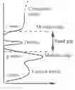
FIG. 2 is a graph illustrating density of states (DOS) function in amorphous semiconductors, featuring the presence of defect states near mid-bandgap and mobility edges which separate extended and localized states;
FIG. 3 is a schematic diagram illustrating carrier hopping conduction in amorphous semiconductors, which is a low mobility process; and
FIGS. 4A-4B are schematic diagrams illustrating the photoconductive process in amorphous and crystalline semiconductors.
DETAILED DESCRIPTION OF THE INVENTION
The invention proposes the use of amorphous alloys as efficient photoconductive detector materials. Amorphous photoconductive alloys such as As—Se—Te—Cu can be deposited using low-cost thermal evaporation or sputtering technique. Processing of these materials is compatible with current Si-CMOS back-end processes, and thus significant cost reduction can be achieved by leverage on the present Si VLSI technology. On the device performance side, two distinctive conduction mechanisms, namely carrier hopping and band conduction are found to be dominant in the amorphous alloys under dark and illuminated conditions, respectively, which leads to a high signal-to-noise ratio (SNR) of photoconductive detectors.
FIG. 1 illustrates a photodiode used in accordance with the invention. The photodiode 2 includes a substrate 8 comprising amorphous semiconductor materials. The substrate 8 has p-type conductivity. Using standard techniques in the art, the substrate 8 is implanted with selective ions to form an n-type region 4 on the substrate 8. The remaining portion 6 of substrate 8 is not implanted and forms the active photodetecting region of the photodiode 2 for detecting an infrared light signal. The regions 4 and 6 form a heterojunction. In other embodiments, the substrate can be doped with n-type conductivity with a p-type region being formed using implantation of selective ions. The amorphous semiconductor materials can include amorphous photoconductive alloys like chalcogenide glass alloys having an alloy arrangement of As—Se—Te—Cu. Using amorphous semiconductor materials allow for high signal-to-noise ratio being achieved by invoking two distinctive conduction mechanisms, namely carrier hopping and band conduction, under dark and illuminated conditions.
According to the well-known Mott-Davis model, density of states (DOS) in amorphous semiconductors is schematically represented in FIG. 2. The DOS function has two distinct features compared to their crystalline counterparts: i) The appearance of mobility edges which separate extended states in the bands from the localized states within the bandgap; ii) The existence of electronic states in mid-bandgap region due to coordination defects, for example, dangling bonds. Extended states in the bands contribute to the electrical conductivity through band conduction, similar to electronic conduction in crystalline semiconductors, and mid-gap defects contribute to the electrical conductivity by carrier hopping from one defect site to another.
Band conduction usually features high mobility, since the movement of electrons or holes in the bands is only limited by scattering events; In contrast, during hopping, thermal excitation or quantum tunneling between defect sites 14 is necessary to obtain mobile carriers because such carriers have to overcome significant energy barriers, as shown in FIG. 3. Hopping is characterized by low mobility and hence low conduction. Conductivity σ in semiconductors is related to carrier mobility μ by:
σ = ∑ i N i q μ i EQ . 1
in which Ni is the concentration of the i'th carrier and q is the carrier charge. Thus higher mobility suggests higher conductivity for the same concentration of carriers.
The invention capitalizes on the difference between carrier mobility in the two conduction regimes to achieve high signal-to-noise ratio in photoconductive detectors. In amorphous solids, the existence of high concentration of coordination defects leads to the dominance of hopping even in room temperature. When illuminated, carriers localized near the defects 14 can be excited into conduction band via absorption of photons. The consequence of the photo excitation process is the presence of non-equilibrium carriers. Unlike carriers localized near defects, these photo-generated carriers are delocalized before they recombine and thus have high mobility, which leads to a large change in conductivity of the semiconductor material.
A schematic illustration comparing the photoconductive process in amorphous and crystalline semiconductors is shown in FIGS. 4A-4B. FIG. 4A illustrates the photoconductivity in crystalline semiconductors. Electron-hole pairs are generated by photon absorption and contribute to photoconductivity. In crystalline semiconductors, both, conduction in the dark and under illumination is carried out by delocalized carriers in the bands. The energy of the absorbed incident photons corresponds to the energy difference between conduction and valence bands.
FIG. 4B illustrates photoconductivity in amorphous semiconductors. Dark conductivity takes place via low-mobility carrier hopping and thus dark conductivity in amorphous solids is much smaller than dark conductivity in crystalline semiconductors. Upon illumination, generated photo carriers are promoted into the conduction band and hence have high mobility, which guarantees a high photocurrent signal for photoconductors. The energy of the incident photons equals the energy difference between Fermi level and defect levels 20, for example, about half of the bandgap in the case shown in FIG. 4B.
Band conduction and hopping exhibit different temperature dependence and thus conduction mechanisms in semiconductors can be experimentally verified by measuring conductivity vs. temperature. Band conduction is characterized by the Arrhenius equation: σ=σ1[exp(ΔE/kT)]−1, where ΔE represents thermal excitation energy (equals the energy difference between Fermi level and band edge in the case of crystalline semiconductors) and k is the Boltzmann constant. Variable range hopping is featured by the well-known T−1/4 law: σ=σ0 exp(T0/T)−1/4 where σ and T represent electrical conductivity and temperature in Kelvin respectively, and σ0 and T0 are two constants that relate material band structures to electrical properties.
Although the present invention has been shown and described with respect to several preferred embodiments thereof, various changes, omissions and additions to the form and detail thereof, may be made therein, without departing from the spirit and scope of the invention.
Claims
What is claimed is:1. An infrared photodiode structure comprising:
a doped semiconductor layer comprising of ions of certain conductivity; and
an active photodetecting region positioned on said doped semiconductor layer for detecting an infrared light signal, said active photodetecting region comprising one or more amorphous semiconductor materials so as to allow for high signal-to-noise ratio being achieved by invoking carrier hopping and band conduction, under dark and illuminated conditions.
2. The infrared photodiode structure of claim 1, wherein said one or more amorphous semiconductor materials comprise chalcogenide glass alloys.
3. The infrared photodiode structure of claim 2, wherein said chalcogenide glass alloys comprise As—Se—Te—Cu material composition.
4. The infrared photodiode structure of claim 1, wherein said carrier hopping takes place between defect sites in said one or more amorphous semiconductor materials.
5. The infrared photodiode structure of claim 1, wherein said one or more amorphous semiconductor materials comprise defects originate from either structural disorder or coordination defects
6. A method of forming infrared photodiode structure comprising:
providing a doped semiconductor layer comprising of ions of certain conductivity;
positioning an active photodetecting region on said doped semiconductor layer for detecting an infrared light signal, said active photodetecting region comprising one or more amorphous semiconductor materials so as to allow for high signal-to-noise ratio being achieved by invoking carrier hopping and band conduction, under dark and illuminated conditions.
7. The method of claim 6, wherein said one or more amorphous semiconductor materials comprise chalcogenide glass alloys.
8. The method of claim 7, wherein said chalcogenide glass alloys comprise As—Se—Te—Cu material composition.
9. The method of claim 6, wherein said carrier hopping takes place between defect sites in said one or more amorphous semiconductor materials.
10. The method of claim 6, wherein said one or more amorphous semiconductor materials comprise defects originate from either structural disorder or coordination defects.
Images & Drawings included:


Sources:
- United States Patent and Trademark Office - verify current appl. status at the USPTO↗
Recent applications in this class:
- » 20250022978 2025-01-16
SHORT-WAVE INFRA-RED RADIATION DETECTION DEVICE - » 20240372027 2024-11-07
High-Power Photodiode Structure and Related Methods of Manufacture - » 20240313145 2024-09-19
LIGHT RECEIVING ELEMENT - » 20240290902 2024-08-29
PHOTO-DETECTING DEVICE - » 20240290901 2024-08-29
HIGHLY-EFFICIENT FULL VAN DER WAALS 1D p-Te/2D n-Bi2O2Se HETERODIODES WITH NANOSCALE ULTRA-PHOTOSENSITIVE CHANNELS - » 20240178338 2024-05-30
PHOTOELECTRIC CONVERSION ELEMENT AND METHOD FOR MANUFACTURING PHOTOELECTRIC CONVERSION ELEMENT - » 20240154053 2024-05-09
GE ON SI PHOTODETECTOR WITH GAIN - » 20240113247 2024-04-04
Infrared detecting device - » 20240088320 2024-03-14
BIO-SENSING DEVICE WITH OPTOELECTRONIC DEVICE - » 20230395742 2023-12-07
OPTICAL SENSOR HAVING 2D-3D HETEROJUNCTION STRUCTURE AND MANUFACTURING METHOD THEREOF
Recent applications for this Assignee:
- » 20250288624 2025-09-18
LONG-TERM STABILIZATION, FORMULATION AND TABLETING OF LIVE MICROBIAL CELLS - » 20250284856 2025-09-11
GENERALIZABLE END-TO-END AUTONOMOUS DRIVING WITH MULTI-MODAL FOUNDATION MODELS - » 20250283816 2025-09-11
COMPOSITIONS FOR DETECTION OF FLUOROCARBONS AND RELATED ARTICLES, SYSTEMS, AND METHODS - » 20250281931 2025-09-11
High-Throughput Expansion Microscopy, Devices for Use With a Well Plate and Methods for Processing a Sample - » 20250278625 2025-09-04
VISUOMOTOR POLICY LEARNING VIA ACTION DIFFUSION - » 20250275716 2025-09-04
SENSORIZED WEARABLE GARMENT - » 20250275026 2025-08-28
ELECTRICALLY CONDUCTIVE FIREBRICK SYSTEM - » 20250263824 2025-08-21
ADDITIVELY MANUFACTURED OXIDE DISPERSION-STRENGTHENED ALLOY - » 20250261881 2025-08-21
FLEXIBLE ELECTRONICS FOR ANALYTE DETECTION - » 20250257316 2025-08-14
CONTROL OF NITROGEN FIXATION IN RHIZOBIA THAT ASSOCIATE WITH CEREALS