Method and structure of monolithically integrated infrared sensing device
US20100187580A1
2010-07-29
12/511,004
2009-07-28
✅ Patent granted
US 8,120,076 B2
2012-02-21
-
-
Jarrett Stark
2029-10-04
Abstract:
Protection for infrared sensing device, and more particularly, to a monolithically integrated uncooled infrared sensing device using IC foundry compatible processes. The proposed infrared sensing device is fabricated on a completed IC substrate. In an embodiment, the infrared sensing device has a single crystal silicon plate with an absorbing layer supported a pair of springs. The absorbing layer absorbs infrared radiation and heats up the underlying silicon layer. As a result, an n well in the silicon layer changes its resistance related to its temperature coefficient of resistance (TCR). In another embodiment, the infrared sensing device has a top sensing plate supported by an underlying spring structures. The top sensing plate has sensing materials such as amorphous silicon, poly silicon, SiC, SiGe, Vanadium oxide, or YbaCuO. Finally, a micro lens array is placed on top of the sensing pixel array with a gap in between. In an embodiment, the micro lens array is fabricated on a silicon substrate and bonded to the sensing pixel array substrate. In another embodiment, the micro lens array is fabricated monolithically using amorphous silicon. The micro lens array layer encapsulates the pixel sensing array hermetically, preferably in a vacuum environment.
Interested in similar patents?
Get notified when new applications in this technology area are published.
Classification:
H01L27/14669 » CPC main
Devices consisting of a plurality of semiconductor or other solid-state components formed in or on a common substrate including semiconductor components sensitive to infra-red radiation, light, electromagnetic radiation of shorter wavelength or corpuscular radiation and specially adapted either for the conversion of the energy of such radiation into electrical energy or for the control of electrical energy by such radiation; Devices controlled by radiation; Imager structures; Imagers using a photoconductor layer Infra-red imagers
H01L27/14692 » CPC further
Devices consisting of a plurality of semiconductor or other solid-state components formed in or on a common substrate including semiconductor components sensitive to infra-red radiation, light, electromagnetic radiation of shorter wavelength or corpuscular radiation and specially adapted either for the conversion of the energy of such radiation into electrical energy or for the control of electrical energy by such radiation; Devices controlled by radiation; Imager structures; Processes or apparatus peculiar to the manufacture or treatment of these devices or parts thereof Thin film technologies, e.g. amorphous, poly, micro- or nanocrystalline silicon
H01L27/14627 » CPC further
Devices consisting of a plurality of semiconductor or other solid-state components formed in or on a common substrate including semiconductor components sensitive to infra-red radiation, light, electromagnetic radiation of shorter wavelength or corpuscular radiation and specially adapted either for the conversion of the energy of such radiation into electrical energy or for the control of electrical energy by such radiation; Devices controlled by radiation; Imager structures; Structural or functional details thereof; Optical elements or arrangements associated with the device Microlenses
H01L27/14685 » CPC further
Devices consisting of a plurality of semiconductor or other solid-state components formed in or on a common substrate including semiconductor components sensitive to infra-red radiation, light, electromagnetic radiation of shorter wavelength or corpuscular radiation and specially adapted either for the conversion of the energy of such radiation into electrical energy or for the control of electrical energy by such radiation; Devices controlled by radiation; Imager structures; Processes or apparatus peculiar to the manufacture or treatment of these devices or parts thereof Process for coatings or optical elements
H01L31/09 IPC
Semiconductor devices sensitive to infra-red radiation, light, electromagnetic radiation of shorter wavelength or corpuscular radiation and specially adapted either for the conversion of the energy of such radiation into electrical energy or for the control of electrical energy by such radiation; Processes or apparatus specially adapted for the manufacture or treatment thereof or of parts thereof; Details thereof in which radiation controls flow of current through the device, e.g. photoresistors Devices sensitive to infra-red, visible or ultraviolet radiation
H01L31/02 IPC
Semiconductor devices sensitive to infra-red radiation, light, electromagnetic radiation of shorter wavelength or corpuscular radiation and specially adapted either for the conversion of the energy of such radiation into electrical energy or for the control of electrical energy by such radiation; Processes or apparatus specially adapted for the manufacture or treatment thereof or of parts thereof; Details thereof Details
H01L31/062 IPC
Semiconductor devices sensitive to infra-red radiation, light, electromagnetic radiation of shorter wavelength or corpuscular radiation and specially adapted either for the conversion of the energy of such radiation into electrical energy or for the control of electrical energy by such radiation; Processes or apparatus specially adapted for the manufacture or treatment thereof or of parts thereof; Details thereof adapted as photovoltaic [PV] conversion devices characterised by at least one potential-jump barrier or surface barrier the potential barriers being only of the metal-insulator-semiconductor type
H01L31/113 IPC
Semiconductor devices sensitive to infra-red radiation, light, electromagnetic radiation of shorter wavelength or corpuscular radiation and specially adapted either for the conversion of the energy of such radiation into electrical energy or for the control of electrical energy by such radiation; Processes or apparatus specially adapted for the manufacture or treatment thereof or of parts thereof; Details thereof in which radiation controls flow of current through the device, e.g. photoresistors characterised by at least one potential-jump barrier or surface barrier, e.g. phototransistors; Devices sensitive to infra-red, visible or ultra-violet radiation characterised by field-effect operation, e.g. junction field-effect phototransistor being of the conductor-insulator-semiconductor type, e.g. metal-insulator-semiconductor field-effect transistor
Description
CROSS-REFERENCES TO RELATED APPLICATIONS
This application claims priority to U.S. Provisional Patent Application Ser. No. 61/084,223, filed Jul. 28, 2008, entitled “METHOD AND STRUCTURE OF MONOLITHICALLY INTEGRATED INFRARED SENSING DEVICE” by inventor XIAO (CHARLES) YANG commonly assigned and incorporated by reference herein for all purposes.
STATEMENT AS TO RIGHTS TO INVENTIONS MADE UNDER FEDERALLY SPONSORED RESEARCH AND DEVELOPMENT
NOT APPLICABLE
REFERENCE TO A “SEQUENCE LISTING,” A TABLE, OR A COMPUTER PROGRAM LISTING APPENDIX SUBMITTED ON A COMPACT DISK.
NOT APPLICABLE
BACKGROUND OF THE INVENTION
This present invention relates in general to protection of infrared sensing device, and more particularly, to a monolithically integrated uncooled infrared sensing device using IC foundry compatible processes.
Uncooled infrared detectors have recently gained wide attention for infrared imaging applications, due to their advantages such as low cost, low weight, low power, large spectral response, and long-term operation compared to those of photon detectors. Worldwide effort is still continuing to implement very large format arrays at low cost for use in various applications, including commercial applications such as driver's night vision enhancement and fire fighting. One of the main issues for achieving low-cost detectors is their monolithic integration and compatibility with CMOS technology.
The most widely used uncooled detector approach is to implement microbolometers using surface micromachined bridges on CMOS processed wafers, where infrared radiation increases the temperature of a material formed on the thermally isolated and suspended bridge, causing a change in its resistance related to its temperature coefficient of resistance (TCR). Vanadium oxide, which is the most widely known and used microbolometer material, has a high TCR of about 2-3%/K; however, Vanadium oxide is not a standard material in IC fabrication and requires dedicated expensive equipment to prevent contamination of the CMOS line. In addition, it exhibits large noise due to its monocrystalline structure. There are efforts to implement surface micromachined microbolometers using IC compatible materials such as amorphous silicon, amorphous silicon carbide, and polycrystalline silicon-germanium; and these materials also have high TCR values of 2.5%/K, 4-6%/K, and 2-3%/K, respectively. However, these materials require high temperature annealing to reduce their residual stress, which is not suitable for post-CMOS processing for monolithic integration. In addition, they exhibit even higher noise than Vanadium oxide due to their monocrystalline structures.
Thus, it is desirable to improve incumbent infrared sensing devices.
BRIEF SUMMARY OF THE INVENTION
This present invention relates in general to protection of infrared sensing device, and more particularly, to a monolithically integrated uncooled infrared sensing device using IC foundry compatible processes.
The proposed infrared sensing device is fabricated on a completed IC substrate. In an embodiment, the infrared sensing device comprises single crystal silicon plate with an absorbing layer supported a pair of springs. The absorbing layer absorbs infrared radiation and heats up the underlying silicon layer. As a result, a n well in the silicon layer changes its resistance related to its temperature coefficient of resistance (TCR). In another embodiment, the infrared sensing device comprises a top sensing plate supported by an underlying spring structures. The top sensing plate has sensing materials such as amorphous silicon, poly silicon, SiC, SiGe, Vanadium oxide, or YbaCuO. Finally, a micro lens array is placed on top of the sensing pixel array with a gap in between. In an embodiment, the micro lens array is fabricated on a silicon substrate and bonded to the sensing pixel array substrate. In another embodiment, the micro lens array is fabricated monolithically using amorphous silicon. The micro lens array layer encapsulates the pixel sensing array hermetically, preferably in a vacuum environment.
DETAILED DESCRIPTION OF THE INVENTION
According to the present invention, techniques for fabricating infrared sensing device are provided. More particularly, the invention includes a method and structure for fabricating infrared sensing device with IC foundry compatible processes. Merely by way of example, the invention has been applied to fabricating infrared sensing device. But it would be recognized that the invention has a much broader range of applicability.
FIG. 1 is a simplified diagram illustrating components of an infrared sensing device according to one embodiment of the present invention. The following diagrams are merely examples, which should not unduly limit the scope of the claims herein. One of ordinary skill in the art would recognize many variations, alternatives, and modifications.
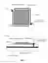
As illustrated, the infrared sensing device has a single crystal silicon plate with an absorbing layer supported a pair of springs. As shown in A-A cross section view, the springs are anchored to the substrate and electrically connected to the top metal through VIAs. The absorbing layer absorbs infrared radiation and heats up the underlying silicon layer. As a result, a n-well in the silicon layer changes its resistance related to its temperature coefficient of resistance (TCR). The change in resistance is detected by the underlying integrated circuits.
FIG. 2 is a simplified diagram illustrating components of an infrared sensing device according to one embodiment of the present invention. Infrared sensing device has a top sensing plate supported by an underlying spring structures. The top sensing plate has sensing materials such as amorphous silicon, poly silicon, SiC, SiGe, Vanadium oxide, or YbaCuO, among others. As shown in A-A cross section view, the top plate is connected to the spring structures via posts. The springs are anchored to the substrate and electrically connected to the top metal through VIAs.
FIG. 3 is a simplified diagram illustrating components of an infrared sensing device according to one embodiment of the present invention. Infrared sensing device has a sensing plate supported by an underlying spring structures. The sensing plate has a top layer and a bottom layer. The top layer is a CCD or CMOS imaging element that sense visible wavelength. The bottom layer is an infrared sensing material such as amorphous silicon, poly silicon, SiC, SiGe, Vanadium oxide, or YbaCuO, among others. As shown in A-A cross section view, the top layer is mechanically and electrically connected to one pair of spring structures; and the bottom layer is mechanically and electrically connected to the other pair of spring structures. The springs are anchored to the substrate and electrically connected to the top metal through VIAs.
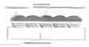
FIG. 4 is a simplified block diagram illustrating of an array of infrared sensing devices according to one embodiment of the present invention. As depicted, an array of infrared sensing elements or pixels is fabricated on top of the IC substrate. A micro lens array is placed on top of the sensing pixel array with a gap in between. In an embodiment, the micro lens array is fabricated on a silicon substrate and bonded to the sensing pixel array substrate. In another embodiment, the micro lens array is fabricated monolithically using amorphous silicon. The micro lens array layer encapsulates the pixel sensing array hermetically, preferably in a vacuum environment.
It is also understood that the examples and embodiments described herein are for illustrative purposes only and that various modifications or changes in light thereof will be suggested to persons skilled in the art and are to be included within the spirit and purview of this application and scope of the appended claims.
Claims
What is claimed is:1. An integrated imager and CMOS integrated circuit device comprising:
a semiconductor substrate having a surface region;
a CMOS integrated circuit device region overlying the surface region;
a dielectric material overlying the CMOS integrated circuit device region;
a plurality of infrared pixel regions, each of the plurality of infrared pixel regions having a suspension member coupled to an input region; and
a plurality of lens devices coupled respectively to the plurality of infrared pixel regions.
2. The device of claim 1 wherein each of the plurality of infrared pixel regions comprises a single crystal silicon n-well region and an overlying absorber material.
3. The device of claim 1 wherein each of the plurality of infrared pixel regions comprises a material selected from amorphous silicon, polysilicon, silicon carbide, silicon germanium, vanadium oxide, or YBaCuO.
4. The device of claim 1 further comprising a plurality of pixel elements capable of detecting light in a visible spectrum range, the plurality of pixel elements respectively coupled to the plurality of infrared pixel elements, each of the plurality of pixel elements overlying at least a portion or an entirety of at least one of the infrared pixel element.
5. The device of claim 1 wherein the plurality of lens devices are formed from amorphous silicon, polysilicon, or single crystal silicon.
6. The device of claim 1 wherein the plurality of lens device are bonded to a support structure to enclose the plurality of infrared pixel regions.
7. The device of claim 1 wherein the plurality of lens device are formed from deposited amorphous silicon.
Images & Drawings included:


Sources:
- United States Patent and Trademark Office - verify current appl. status at the USPTO↗
Recent applications in this class:
- » 20240339482 2024-10-10
Microbolometer systems and methods - » 20240186361 2024-06-06
VISIBLE AND INFRARED IMAGE SENSOR - » 20240162272 2024-05-16
MICROBOLOMETER SYSTEMS AND METHODS - » 20230223420 2023-07-13
Light receiving element and electronic apparatus - » 20220068992 2022-03-03
Terahertz detector based on Schottky contact rasterization structure - » 20220013573 2022-01-13
Electromagnetic radiation detection structure with optimised absorption and method for forming such a structure - » 20210159263 2021-05-27
CMOS cap for MEMS devices - » 20210126038 2021-04-29
Scalable thermoelectric-based infrared detector - » 20200321386 2020-10-08
Light receiving element and electronic apparatus - » 20200295077 2020-09-17
Infrared detection film, infrared detection sensor and infrared detection display apparatus including the infrared detection film, and method of making the infrared detection film