Electrical connector having improved restricting portions
US20100248519A1
2010-09-30
12/750,599
2010-03-30
✅ Patent granted
US 7,993,152 B2
2011-08-09
-
-
Hien Vu
2030-03-30
Abstract:
An electrical connector (100) electrically connects a chip of a first width. The electrical connector includes an insulative housing (2), a number of contacts (3), a connecting member (4), and an actuator (5) mounted on the insulative housing. The connecting member has a connecting region electrically connectable with the chip. The connecting region has a second width not less than the first width. The actuator is formed with a pair of first side walls (51) and a pair of restricting portions (514) respectively protruding inwardly from the pair of first side walls. The pair of restricting portions are spaced a distance substantially equal to the second width to guidingly restrict the chip in the connecting region.
Assignee:
- HON HAI PRECISION INDUSTRY CO., LTD. 12,833 🇹🇼 Tu-Cheng, Taiwan
- Hon Hai Precision Ind. Co., Ltd. 546 🇹🇼 New Taipei, Taiwan
Interested in similar patents?
Get notified when new applications in this technology area are published.
Classification:
H01R11/22 IPC
Individual connecting elements providing two or more spaced connecting locations for conductive members which are, or may be, thereby interconnected, e.g. end pieces for wires or cables supported by the wire or cable and having means for facilitating electrical connection to some other wire, terminal, or conductive member, blocks of binding posts; End pieces or tapping pieces for wires, supported by the wire and for facilitating electrical connection to some other wire, terminal or conductive member End pieces terminating in a spring clip
H05K7/1023 » CPC main
Constructional details common to different types of electric apparatus; Arrangements of circuit components or wiring on supporting structure; Plug-in assemblages of components, e.g. IC sockets having exterior leads co-operating by abutting, e.g. flat pack
H05K7/1023 » CPC main
Constructional details common to different types of electric apparatus; Arrangements of circuit components or wiring on supporting structure; Plug-in assemblages of components, e.g. IC sockets having exterior leads co-operating by abutting, e.g. flat pack
G01R1/0466 » CPC further
Details of instruments or arrangements of the types included in groups - and; General constructional details; Housings; Supporting members; Arrangements of terminals; Test fixtures or contact fields; Connectors or connecting adaptors; Test clips; Test sockets; Sockets for IC's or transistors; Details concerning contact pieces or mechanical details, e.g. hinges or cams; Shielding
H01R13/193 » CPC further
Details of coupling devices of the kinds covered by groups or -; Contact members Means for increasing contact pressure at the end of engagement of coupling part, e.g. zero insertion force or no friction
H01R13/62 IPC
Details of coupling devices of the kinds covered by groups or - Means for facilitating engagement or disengagement of coupling parts or for holding them in engagement
Description
BACKGROUND OF THE INVENTION
1. Field of the invention
The present invention relates to an electrical connector, and more particularly to a test socket having restricting portions restricting the chips at the predetermined position.
2. Description of Related Art
U.S. Pat. No. 7,121,858 issued to Chen on Oct. 17, 2006 discloses an electrical connector. The electrical connector comprises an insulative housing, a connecting member and an actuator mounted on the insulative housing, and a pair of springs mounted between the actuator and the insulative housing. The connecting member has a connecting region connectable with the chip. During the insertion process, when the actuator is pushed downwardly, the chip is located on the connecting region.
A locating space surrounded by the inner faces of the actuator is larger than the connecting region. During the insertion process, the chip is apt to be located at an undesired position out of the connecting region. It would result in unreliable connection between the chip and the electrical connector.
Hence, an electrical connector formed with an improved restricting portion is desired to overcome the above-mentioned disadvantages of the related art.
SUMMARY OF THE INVENTION
An object of the present invention is to provide a burn-in test socket having improved restricting portions restricting the chip at a predetermined position.
To achieve the aforementioned objects, an electrical connector electrically connecting a chip of a first width includes an insulative housing defining a plurality of contact recesses, a plurality of contacts inserted in the contact recesses, a connecting member and an actuator. The connecting member is mounted on the insulative housing and has a connecting region electrically connectable with the chip. The connecting region has a second width not less than the first width. The actuator is moveably assembled to the insulative housing. The actuator is formed with a pair of first side walls and a pair of restricting portions respectively protruding inwardly from the pair of first side walls. The pair of restricting portions are spaced a distance substantially equal to the second width to guidingly restrict the chip in the connecting region.
The electrical connector could be connected with two types of IC package having different widths, in a condition that the guiding members are assembled to or disassembled from the connecting member. The guiding members could be designed into different dimensions to guide in different types of IC package.
Other objects, advantages and novel features of the invention will become more apparent from the following detailed description of a preferred embodiment when taken in conjunction with the accompanying drawings.
BRIEF DESCRIPTION OF THE DRAWINGS
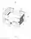
FIG. 1 is an assembled perspective view showing an electrical connector in an initial position in accordance with the present invention;
FIG. 2 is an assembled perspective view similar to FIG. 1, taken from another aspect;
FIG. 3 is an assembled perspective view showing the electrical connector in a depressed position;
FIG. 4 is an exploded perspective view of the electrical connector as shown in FIG. 1;
FIG. 5 is a cross-sectional view of the electrical connector, taken along line 5-5 of FIG. 1, when the electrical connector is located in a closed position, with the IC package being left out; and
FIG. 6 is a cross-sectional view of the electrical connector, taken along line 6-6 of FIG. 3, when the electrical connector is located in an opened position, with the IC package being left out.
DETAILED DESCRIPTION OF THE INVENTION
Reference will now be made to the drawing figures to describe the present invention in detail. Referring to FIGS. 1-5, an electrical connector 100 in accordance with the preferred embodiment of the present invention is adapted for electrically connecting with a chip 6. The chip 6 is formed with a plurality of conductive tails 61. The electrical connector 100 comprises an insulative housing 2, a plurality of contacts 3, a pair of springs 23, a connecting member 4 and an actuator 5.
Referring to FIGS. 2 and 3, the insulative housing 2 comprises a base 27 having a pair of first side faces 271 and a pair of second side faces 272. The base 27 defines a plurality of latching recesses 21 and a plurality of through holes 24 at the outer side of the latching recesses 21. The insulative housing 2 defines a plurality of contact recesses 20 at the first side faces 271 for insertion of the contacts 3. The insulative housing 2 defines a plurality of sliding recesses 25 at the second side faces 272. Each sliding recess 25 has a blocking portion 26 formed therein. The insulative housing 2 has an opening 28 defined on each second side face 272 between two sliding recesses 25. The opening 28 is formed with an upwardly extending protrusion 22.
The contact 3 comprises a body portion 30, a soldering portion 32 formed at the bottom of the body portion 30, a first and a second beams 33, 34 extending from the body portion 30. The second beam 34 is located above the first beam 33 and comprises a first branch 341 and a second branch 342. The second branch 342 is located between the first branch 341 and the first beam 33.
The connecting member 4 comprises a connecting wall 40, a pair of primary walls 41 rising from opposite sides of the connecting wall 40, and a plurality of periphery walls 42 rising from the connecting wall 40. Each periphery wall 42 is connected to a respective side edge of the primary wall 41. The connecting member 4 has a plurality of latching beams 43 extending downwardly from the connecting wall 40. The connecting wall 40 has a plurality of slits 401 communicating with the contact recesses 20 defined adjacent to the primary walls 41 for corresponding to the contacts 3. The periphery wall 42 defines a cutout 45 therein. The periphery wall 42 comprises a vertical first inner face 421 and an inclined face 422 extending from the first inner face 421.
The actuator 5 comprises a pair of first side walls 51 and a pair of second side walls 52 connected together. The first side wall 51 is formed with a restricting portion 514 protruding inwardly from the first side wall 51. The restricting portion 514 is formed with a pair of guiding faces 5141 and a second inner face 5142 below the guiding face 5141. The second side wall 52 defines a plurality of contact slots 50 communicating with corresponding contact recesses 20 of the insulative housing 2. The actuator 5 is formed with a plurality of downwardly extending sliding beams 53.
Referring to FIGS. 1 and 5, in assembling of the electrical connector 100, the contacts 3 are inserted in the contact recesses 20, and the springs 23 are encircled around the protrusions 22. The connecting member 4 is mounted on the insulative housing 2, with the latching beams 43 latching with the latching recesses 21. The actuator 5 is floatably mounted on the insulative housing 2 and supported by the springs 23, with the sliding beams 53 slidable in the sliding recesses 25. The restricting portions 514 are disposed in the cutouts 45. The second inner face 5142 of the actuator 5 is coplanar with corresponding first inner face 421 of the connecting member 4. In conjunction with FIG. 4, the first branch 341 of the contact 3 is secured in the contact slot 50 of the actuator 5.
FIGS. 3 and 6 show the depressed electrical connector 100. When the actuator 5 is actuated downwardly, the first branches 341 of the contacts 3 are depressed by the actuator 5 and slide along an oblique face 54 of the actuator 5 to an opened position as shown in FIG. 5. The chip 6 is put into the connecting member 4.
FIGS. 1 and 5 show the initial electrical connector 100, i.e., the restored electrical connector 100. When the actuator 5 is released, the actuator 5 restores to the initial position as shown in FIG. 4, under the resilient force provided by the springs 23. The second branch 342 and the first beam 33 clamp and electrically connect with the conductive tails 61 of the chip 6. The sliding beams 53 of the actuator 5 slide along the sliding recesses 25 and are blocked by the blocking portions 26.
Referring to FIG. 4, a locating region of the connecting wall 40 has a width A between the pair of inclined faces 422 of the periphery walls 42 of the connecting member 4. An effective connecting region has a width B between the pair of first inner faces 421 of the periphery walls 42. The width B is smaller than the width A. A distance between the second inner faces 5142 of the pair of restricting portions 514 is equal to the width B. It is possible that the chip 6 is disdodged at an undesired position of the locating region, i.e., not in the connecting region. However, during the restoring process, when the chip 6 is located at the undesired position, the chip 6 would be guided by the guiding faces 5141 of the restricting portions 514 of the upwardly restoring actuator 5. The chip 6 would be finally restricted in the connecting region between the pair of restricting portions 514, since the distance between the pair of the second inner faces 5142 of the restricting portions 514 is equal to the width B of the effective connecting region, when the actuator 5 is restored to the initial position.
However, the disclosure is illustrative only, changes may be made in detail, especially in matter of shape, size, and arrangement of parts within the principles of the invention.
Claims
What is claimed is:1. An electrical connector for electrically connecting a chip of a first width, comprising:
an insulative housing defining a plurality of contact recesses;
a plurality of contacts inserted in the contact recesses;
a connecting member mounted on the insulative housing and having a connecting region electrically connectable with the chip, said connecting region having a second width not less than the first width; and
an actuator moveably assembled to the insulative housing, said actuator being formed with a pair of first side walls and a pair of restricting portions respectively protruding inwardly from the pair of first side walls, the pair of restricting portions being spaced a distance substantially equal to the second width to guidingly restrict the chip in the connecting region.
2. The electrical connector as claimed in claim 1, wherein each restricting portion is formed with a guiding face for guiding the chip into the connecting region.
3. The electrical connector as claimed in claim 1, wherein said connecting member comprises a pair of periphery walls each having a first inner face and an inclined face extending from the first inner face, and said restricting portion has a second inner face substantially coplanar with the first inner face.
4. The electrical connector as claimed in claim 3, wherein each periphery wall of the connecting member defines a cutout corresponding to the restricting portion.
5. The electrical connector as claimed in claim 3, wherein said connecting member comprises a connecting wall, said connecting region being defined on the connecting wall.
6. The electrical connector as claimed in claim 5, wherein said connecting member comprises a pair of primary walls each defining a plurality of slits for insertion of the contacts, said pair of primary walls and the pair of periphery walls rising from the connecting wall.
7. The electrical connector as claimed in claim 5, wherein said insulative housing defines a plurality of latching recesses, said connecting member comprising a plurality of latching beams extending downwardly from the connecting wall for latching with the latching recesses.
8. The electrical connector as claimed in claim 1, further comprising a plurality of springs mounted between the insulative housing and the actuator for supporting the actuator.
9. The electrical connector as claimed in claim 1, wherein said insulative housing defines a plurality of sliding recesses and a plurality of blocking portions each formed in an associated sliding recess, and wherein said actuator is formed with a plurality of sliding beams each slidable in the sliding recess and blocked by the blocking portion.
10. The electrical connector as claimed in claim 1, wherein said contact comprises a body portion, a first and a second beams extending from the body portion for clamping and electrically connecting with the chip.
11. The electrical connector as claimed in claim 10, wherein said actuator is formed with a plurality of contact slots communicating with the contact recesses, said second beam of the contact comprising a first branch secured in the contact slot.
12. The electrical connector as claimed in claim 11, wherein said second beam of the contact comprises a second branch located between the first branch and the first beam, said first branch being operable by the actuator to urge the second branch and the first beam to engage with or disengage from the chip.
13. An electrical connector comprising:
an insulative housing defining a plurality of contact recesses;
a plurality of contacts disposed in the corresponding contact recesses, respectively;
a connecting member mounted upon the housing and defining a plurality of slits in alignment with the corresponding contact recesses, respectively, to allow the corresponding contacts to extend thereinto;
an actuator up and down moveably mounted upon the connecting member and defining a plurality of contact slots in alignment with the corresponding contact recesses and slits, respectively;
the connecting member defining a plurality of periphery walls to define an electronic component receiving cavity with a pair of cutouts formed in two opposite side periphery walls;
the actuator including a pair of corresponding side walls with thereon a pair of protrusions received in the corresponding cutouts; wherein
each of the periphery walls defines an upper oblique guiding section and a lower vertical section for stationary guidable reception of an electronic component in the electronic component receiving cavity, and each of the protrusions defines an upper oblique guiding portion and lower vertical portion for dynamic guidable reception of the electronic component in the electronic component receiving cavity.
14. The electrical connector as claimed in claim 13, wherein the actuator pushes the corresponding contacts outwardly during downward movement thereof.
15. The electrical connector as claimed in claim 13, wherein each of said protrusions forms a notch for facilitating loading/unloading the electronic component with regard to the electronic component receiving cavity.
Images & Drawings included:


Sources:
- United States Patent and Trademark Office - verify current appl. status at the USPTO↗
Recent applications in this class:
- » 20160073535 2016-03-10
High-power electronic module and method for making such a module - » 20100261370 2010-10-14
Semiconductor package socket - » 20100053925 2010-03-04
CHIP MOUNT FOR DATA STORAGE DEVICE - » 20080305656 2008-12-11
Electrical connector assembly with floatably arranged wafer - » 20080012105 2008-01-17
Chip adapter - » 20070218742 2007-09-20
Chip adapter seat - » 20050250363 2005-11-10
Socket for semiconductor device - » 20050068753 2005-03-31
IC socket having fastening mechanism for sensor - » 20050042905 2005-02-24
Contact pin and socket for electrical parts
Recent applications for this Assignee:
- » 20140233961 2014-08-21
Optical communication module including optical-electrical signal converters and optical signal generators - » 20140083669 2014-03-27
HEAT SINK - » 20140063746 2014-03-06
Electronic device with heat dissipation assembly - » 20140061224 2014-03-06
AUTOMATIC VENDING MACHINE - » 20140060914 2014-03-06
Enclosure with shield apparatus - » 20140058727 2014-02-27
MULTIMEDIA RECORDING SYSTEM AND METHOD - » 20140055955 2014-02-27
Fastener - » 20140055322 2014-02-27
DISPLAY SYSTEM AND HEAD-MOUNTED DISPLAY APPARATUS - » 20140054439 2014-02-27
CONTAINER DATA CENTER WITH SUPPORTING APPARATUS - » 20140054311 2014-02-27
AUTOMATIC VENDING MACHINE WITH MOVING MEMBER FOR PRODUCTS