EMI SHIELD SPRING DEVICE
US20100261359A1
2010-10-14
12/752,127
2010-04-01
Abstract:
An electro-magnetic interference device attached to a surface of an object by soldering is disclosed. The device comprises a base comprising a surface defining at least one recessed portion. The at least one recessed portion comprises a side wall. An angle between the side wall and the surface of the base is equal to or greater than 90 degrees.
Assignee:
- HON HAI PRECISION INDUSTRY CO., LTD. 12,828 🇹🇼 Tu-Cheng, Taiwan
- HONG FU JIN PRECISION INDUSTRY (SHENZHEN) CO., LTD. 4,225 🇨🇳 Shenzhen City, China
Interested in similar patents?
Get notified when new applications in this technology area are published.
Classification:
H05K9/0035 » CPC main
Screening of apparatus or components against electric or magnetic fields; Casings with localised screening of components mounted on printed circuit boards [PCB]; Shield cases mounted on a PCB, e.g. cans or caps or conformal shields having multiple parts, e.g. frames mating with lids with retainers mounted beforehand on the PCB, e.g. clips
H05K3/341 » CPC further
Apparatus or processes for manufacturing printed circuits; Assembling printed circuits with electric components, e.g. with resistor electrically connecting electric components or wires to printed circuits by soldering Surface mounted components
H05K3/341 » CPC further
Apparatus or processes for manufacturing printed circuits; Assembling printed circuits with electric components, e.g. with resistor electrically connecting electric components or wires to printed circuits by soldering Surface mounted components
H05K2201/0311 » CPC further
Indexing scheme relating to printed circuits covered by; Conductive materials; Properties and characteristics in general Metallic part with specific elastic properties, e.g. bent piece of metal as electrical contact
H05K2201/0311 » CPC further
Indexing scheme relating to printed circuits covered by; Conductive materials; Properties and characteristics in general Metallic part with specific elastic properties, e.g. bent piece of metal as electrical contact
H05K2201/1031 » CPC further
Indexing scheme relating to printed circuits covered by; Details of components or other objects attached to or integrated in a printed circuit board; Other objects, e.g. metallic pieces Surface mounted metallic connector elements
H05K2201/1031 » CPC further
Indexing scheme relating to printed circuits covered by; Details of components or other objects attached to or integrated in a printed circuit board; Other objects, e.g. metallic pieces Surface mounted metallic connector elements
H05K2201/1084 » CPC further
Indexing scheme relating to printed circuits covered by; Details of components or other objects attached to or integrated in a printed circuit board; Details of electrical connections of non-printed components, e.g. special leads; Details of leads; Shape details Notched leads
Y02P70/50 » CPC further
Climate change mitigation technologies in the production process for final industrial or consumer products Manufacturing or production processes characterised by the final manufactured product
Y02P70/50 » CPC further
Climate change mitigation technologies in the production process for final industrial or consumer products Manufacturing or production processes characterised by the final manufactured product
H01R12/00 IPC
Structural associations of a plurality of mutually-insulated electrical connecting elements, specially adapted for printed circuits, e.g. printed circuit boards [PCBs], flat or ribbon cables, or like generally planar structures, e.g. terminal strips, terminal blocks; Coupling devices specially adapted for printed circuits, flat or ribbon cables, or like generally planar structures; Terminals specially adapted for contact with, or insertion into, printed circuits, flat or ribbon cables, or like generally planar structures
Description
BACKGROUND
1. Technical Field
The present disclosure relates to an electro-magnetic interference (EMI) shield spring device.
2. Description of Related Art
EMI shield spring clips/contacts are known in the art, such as the EMI shield springs described in U.S. Pat. No. 5,532,428 to Radloff et al., U.S. Pat. No. 6,678,170 to Barringer et al., and U.S. Pat. No. 5,225,269 to Garrett. The EMI shield spring clips/contacts can be attached to a circuit board of an electronic device by soldering. However, in certain instances, for example, when the circuit board is small and includes large quantity of electrical components, leaves a small area for contacting and welding the EMI shield springs. As such, EMI shield spring may have a weak connection with the circuit board and tends to disengage.
What is needed is an EMI shield spring device to solve the aforementioned problems.
BRIEF DESCRIPTION OF THE DRAWINGS
The components in the drawings are not necessarily drawn to scale, the emphasis instead being placed upon clearly illustrating the principles of the EMI shield spring device. Moreover, in the drawings, like reference numerals designate corresponding parts throughout the several views.
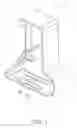
FIG. 1 is an isometric view of a detachable portable shielding device in accordance with an exemplary embodiment.
FIG. 2 is an isometric view of the shielding device in FIG. 1 from a different angle.
FIG. 3 is a cross-sectional view of a connecting surface of the shielding device in FIG. 1, in accordance with a first exemplary embodiment.
FIG. 4 is another cross-sectional view of the connecting surface of the shielding device in FIG. 1, in accordance with a second exemplary embodiment.
DETAILED DESCRIPTION
Referring to FIGS. 1 and 2, a device 10 to be attached to a surface of an object is disclosed in accordance with an exemplary embodiment. In the exemplary embodiment, the device 10 is an electro-magnetic interference (EMI) shield spring clip/contact. The spring clip/contact 10 includes a rectangular base plate 20. In the embodiment, the base plate 20 is made of metallic material and includes a soldering surface 21 defining two recessed portions 22 formed by stamping. The soldering surface 21 is a planar surface.
In the exemplary embodiment, the recessed portions 22 are formed by stamping. The recessed portions 22 extend along the lengthwise direction of the base plate 20. The recessed portions 22 are parallel to each other. The geometry shape of the recessed portions is not limited and may be modified according to need. One aspect influencing the geometry shape and other parameters such as depth is the height of the spring clip/contact 10.
Referring to FIG. 3, the recessed portion 22 includes two sidewalls 23 opposite to each other and a top wall 24 connecting the sidewalls 23. In the exemplary embodiment, an angle M between the side wall 23 and the soldering surface 21 is about 90 degrees.
In another embodiment shown in FIG. 4, the sidewall 23a is angled from the soldering surface 21a. An angle M between the side wall 23a and the soldering surface 21a is greater than 90 degrees. In the embodiment, the angle M is about 135 degrees.
The spring clip/contact 10 can be soldered to the object, such as a circuit board 30 by surface mounting techniques. After the spring clip/contact 10 is soldered to the circuit board 30, a layer of solder is formed between the surface 31 and a surface of the circuit board 30. A certain quantity of solder forms within the recessed portions 22. That is, in addition to the surface 21, the side walls 23 also connect to the surface 31 by solder, which assists to increase the connection strength between the spring clip/contact 10 and the circuit board 30.
It is noteworthy, that the wettability of the surface 31 is important. This gives adhesion and cohesion that result in strong interfacial tension. The smaller the wetting angle of a surface, the greater the wettability of its surface by a specific liquid and vice versa.
Because the angle M is equal to or greater than 90 degrees, the wetting angle or contact angle N, which measured between the side wall 23 and the imaginary line L, is a supplementary angle of the angle M and is equal to or less than 90 degrees. With such structure of the recessed portions 22, the mechanical connection between the spring clip/contact 10 and the circuit board 30 becomes stronger than it otherwise would be.
In the exemplary embodiment, to facilitate the wetting of the surface 31, a through opening 25 is formed between the recessed portions 22. In another embodiment, the top wall 24 may be removed, so that the recessed portions 22 extend through the base plate 20, which assists the wetting of the surface 31.
When the spring clip/contact 10 is shaped to have a dimension of 6.3 mm (length) by 5.5 mm (width) by 2.5 mm (height) by 0.1 mm (thickness), and the recessed portion 22 is shaped to be 2.3 mm (length) by 0.2 mm (width) by 0.15 mm (depth), the connection strength between the spring clip/contact 10 and the circuit board 30 increases by 126%. Comparing to when the spring clip/contact 10 has no such recessed portion.
While various embodiments have been illustrated and described, the disclosure is not to be construed as being limited thereto. Those skilled in the art can make various modifications to the embodiments without departing from the true spirit and scope of the disclosure as defined by the appended claims.
Claims
What is claimed is:1. An electro-magnetic interference (EMI) device for being attached to a surface of an object by soldering, the device comprising:
a base comprising a surface defining at least one recessed portion, the at least one recessed portion comprising a side wall, wherein, an angle between the side wall and the surface of the base is equal to or greater than 90 degrees.
2. The EMI device according to claim 1, wherein the device is shaped as a spring.
3. The EMI device according to claim 1, wherein the number of the at least one recessed portion is two.
4. The EMI device according to claim 1, wherein the surface of the base defines a through opening.
5. The EMI device according to claim 3, wherein the surface of the base defines a through opening, the through opening is formed between the two recessed portions.
6. The EMI device according to claim 1, wherein the surface of the base is planar.
7. The EMI device according to claim 1, wherein the device is made of metallic material and the at least one recessed portion is formed by stamping.
8. The EMI device according to claim 7, wherein the at least one recessed portion extends through the base.
9. The EMI device according to claim 1, wherein the at least one recessed portion extends along the lengthwise direction of the base.
10. The EMI device according to claim 1, wherein each of the at least one recessed portion is elongated with a length of about 2.3 millimeter and a width of about 0.2 millimeter.
Images & Drawings included:


Sources:
- United States Patent and Trademark Office - verify current appl. status at the USPTO↗
Similar patent applications:
- » 20100311254
Electronic device with EMI shield spring device
Recent applications in this class:
- » 20250107055 2025-03-27
ABSORBER FOR PRINTED CIRCUIT BOARD ASSEMBLY - » 20240224481 2024-07-04
Shield Can as Stiffener on Flexible Printed Circuits - » 20220022348 2022-01-20
Shielded interconnect system - » 20200107477 2020-04-02
Terminal and method for retaining a component to a surface, and manufacturing method and apparatus - » 20160081236 2016-03-17
Conductive clip - » 20130148318 2013-06-13
Clip terminal for fixing case and shield apparatus using the same - » 20130008707 2013-01-10
Metal strip assembly for EMI shield case, EMI shield case including the same, and fabrication method of the case - » 20110272188 2011-11-10
Mid-board module retention and EMI cage - » 20090057002 2009-03-05
Shield structure - » 20070035938 2007-02-15
Printed circuit board assembly
Recent applications for this Assignee:
- » 20140233961 2014-08-21
Optical communication module including optical-electrical signal converters and optical signal generators - » 20140083669 2014-03-27
HEAT SINK - » 20140083669 2014-03-27
HEAT SINK - » 20140063746 2014-03-06
Electronic device with heat dissipation assembly - » 20140061224 2014-03-06
AUTOMATIC VENDING MACHINE - » 20140060914 2014-03-06
Enclosure with shield apparatus - » 20140058727 2014-02-27
MULTIMEDIA RECORDING SYSTEM AND METHOD - » 20140055955 2014-02-27
Fastener - » 20140055322 2014-02-27
DISPLAY SYSTEM AND HEAD-MOUNTED DISPLAY APPARATUS - » 20140054439 2014-02-27
CONTAINER DATA CENTER WITH SUPPORTING APPARATUS