MOLDING STAMPER AND METHOD FOR FABRICATING SAME
US20100301517A1
2010-12-02
12/608,164
2009-10-29
Abstract:
An exemplary method for fabricating a molding stamper includes the following steps. Firstly, a master mold having microstructures spaced apart from each other is provided. Secondly, a patterned layer is formed on the microstructures, the patterned layer having molding surfaces apart from each other, and being made of a flexible organic material. Thirdly, the master mold is removed from the patterned layer. Finally, a hard coating layer is deposited on the molding surfaces to form a molding stamper.
Assignee:
- HON HAI PRECISION INDUSTRY CO., LTD. 12,828 🇹🇼 Tu-Cheng, Taiwan
Interested in similar patents?
Get notified when new applications in this technology area are published.
Classification:
B29C33/3857 » CPC main
Moulds or cores; Details thereof or accessories therefor characterised by the material or the manufacturing process; Manufacturing moulds, e.g. shaping the mould surface by machining by making impressions of one or more parts of models, e.g. shaped articles and including possible subsequent assembly of the parts
B29C33/565 » CPC further
Moulds or cores; Details thereof or accessories therefor; Coatings, e.g. enameled or galvanised ; Releasing, lubricating or separating agents Consisting of shell-like structures supported by backing material
B29C43/021 » CPC further
Compression moulding, i.e. applying external pressure to flow the moulding material; Apparatus therefor of articles of definite length, i.e. discrete articles characterised by the shape of the surface
B29D11/00365 » CPC further
Producing optical elements, e.g. lenses or prisms; Production of simple or compound lenses Production of microlenses
G03F7/0017 » CPC further
Photomechanical, e.g. photolithographic, production of textured or patterned surfaces, e.g. printing surfaces; Materials therefor, e.g. comprising photoresists; Apparatus specially adapted therefor for the production of embossing, cutting or similar devices; for the production of casting means
B29C45/2632 » CPC further
Injection moulding, i.e. forcing the required volume of moulding material through a nozzle into a closed mould; Apparatus therefor; Component parts, details or accessories; Auxiliary operations; Moulds with mould wall parts provided with fine grooves or impressions, e.g. for record discs Stampers; Mountings thereof
B29C2043/025 » CPC further
Compression moulding, i.e. applying external pressure to flow the moulding material; Apparatus therefor of articles of definite length, i.e. discrete articles characterised by the shape of the surface having a plurality of grooves forming a microstructure, i.e. fine patterning
B29C2043/3634 » CPC further
Compression moulding, i.e. applying external pressure to flow the moulding material; Apparatus therefor; Component parts, details or accessories; Auxiliary operations; Moulds for making articles of definite length, i.e. discrete articles with pressing members independently movable of the parts for opening or closing the mould, e.g. movable pistons; Forming elements, e.g. mandrels or rams or stampers or pistons or plungers or punching devices having specific surface shape, e.g. grooves, projections, corrugations
B29K2021/00 » CPC further
Use of unspecified rubbers as moulding material
B29L2011/0016 » CPC further
Optical elements, e.g. lenses, prisms Lenses
B29C33/42 IPC
Moulds or cores; Details thereof or accessories therefor characterised by the shape of the moulding surface, e.g. ribs or grooves
B29C59/02 IPC
Surface shaping of articles , e.g. embossing; Apparatus therefor by mechanical means, e.g. pressing
Description
BACKGROUND
1. Technical Field
The present disclosure relates to methods for fabricating molding stampers, and particularly, to a method for fabricating a molding stamper having a pattern for shaping a plurality of microlenses, and a molding stamper fabricated by the method.
2. Description of Related Art
A conventional method for making a molding stamper typically includes the following steps: forming a photoresist layer on a substrate; exposing the photoresist layer to light, and developing the photoresist layer using developer; etching the substrate to form a patterned substrate, and removing the photoresist layer; forming a seed layer on the patterned substrate; electroforming a body on the substrate; and separating the electroformed body from the substrate, and stripping the seed layer off the electroformed body to obtain the molding stamper.
However, this method for fabricating the molding stamper includes many steps, and thus the production efficiency of the molding stamper is rather low. In addition, portions of the seed layer may not be completely stripped off from the electroformed body. When this happens, a surface roughness of the molding stamper is increased. This in turn means that the defect rate of final products made using the molding stamper may be unduly high.
Therefore, what is needed is a new method for fabricating a molding stamper, and a molding stamper fabricated by such method, which can overcome the limitations described.
BRIEF DESCRIPTION OF THE DRAWINGS
Many aspects of the present embodiments can be better understood with reference to the following drawings. The components in the drawings are not necessarily drawn to scale, the emphasis instead being placed upon clearly illustrating the principles of the present embodiments. Moreover, in the drawings, like reference numerals designate corresponding parts throughout the several views.
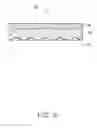
FIG. 1 is a flowchart of a method for fabricating a molding stamper according to an exemplary embodiment.
FIGS. 2-6 illustrate successive stages in fabricating the molding stamper according to the method of FIG. 1.
DETAILED DESCRIPTION
Embodiments will now be described in detail below with reference to the drawings. In this description, unless the context indicates otherwise, it is assumed that a “microstructure” is a structure which has at least one of three dimensions thereof in the range from about 0.1 micrometers to about 999 micrometers. Similarly, unless the context indicates otherwise, a “microlens” is assumed to have a similar meaning.
Referring to FIG. 1, a method for fabricating a molding stamper 50 (see FIG. 6), in accordance with an exemplary embodiment, includes the following steps: step S1, providing a master mold having a plurality of spaced microstructures thereon; step S2, forming a patterned layer on the microstructures, the patterned layer having a plurality of molding surfaces spaced apart from each other, and being made of a flexible organic material; step S3, forming a light transmissive substrate on a surface of the patterned layer, the surface being opposite to the molding surfaces; step S4, removing the master mold from the patterned layer; and step S5, depositing a hard coating layer on the molding surfaces to form a molding stamper, the molding stamper comprising the light transmissive substrate, the patterned layer, and the hard coating layer.
In step S1, referring also to FIG. 2, a master mold 10 is firstly provided. The master mold 10 includes a plurality of microstructures 101 spaced apart from each other. In the present embodiment, the microstructures 101 are made by ultra-precision cutting, and the microstructures 101 are protrusions. In other embodiments, the microstructures 101 may instead be made by electron beam lithography, laser lithography, particle beam lithography, etc; and the microstructures 101 may instead be recesses.
In step S2, referring to FIG. 3, a patterned layer 20 is formed on the microstructures 101 by pouring a flexible organic material over the microstructures 101, and curing the flexible organic material. The patterned layer 20 includes a plurality of molding surfaces 201 at a bottom side thereof, and a surface 202 at an opposite top side thereof. The molding surfaces 201 are spaced apart from each other, and are configured for shaping microlenses (not shown). The molding surfaces 201 are formed by transferring the microstructures 101 onto the flexible organic material, and correspondingly are recesses. In the present embodiment, the patterned layer 20 is made of polydimethyl siloxane (PDMS). In alternative embodiments, the molding surfaces 201 may instead be protrusions. In other alternative embodiments, the patterned layer 20 may instead be made of polymethyl methacrylate (PMMA), polycarbonate (PC), etc.
In step S3, referring to FIG. 4, a light transmissive substrate 30 is formed on the surface 202 of the patterned layer 20. The light transmissive substrate 30 is configured for supporting the patterned layer 20 to facilitate a higher bearing strength of the mold stamper 50.
In step S4, referring to FIG. 5, the master mold 10 is removed from the patterned layer 20.
In step S5, referring to FIG. 6, a hard coating layer 40 is deposited on the molding surfaces 201 and on a bottom surface of the patterned layer 20 that surrounds the molding surfaces 201, thereby forming the molding stamper 50. The molding stamper 50 includes the patterned layer 20, the light transmissive substrate 30, and the hard coating layer 40. The hard coating layer 40 is configured for enhancing the hardness of the molding surfaces 201. In the present embodiment, the hard coating layer 40 is deposited by radio frequency magnetron sputtering, and the hard coating layer 40 is made of silicon dioxide. In other embodiments, the hard coating layer 40 may instead be made of silicon, silicon carbide, diamond-like carbon, etc.
When the hard coating layer 40 is being deposited, a bombardment temperature on a silicon dioxide sputtering target (not shown) is in a range from about 160 degrees Centigrade to about 200 degrees Centigrade. A pressure in a vacuum cavity (not shown) receiving the combined patterned layer 20 and light transmissive substrate 30 therein is in a range from about 0.013332 pascal (Pa) to about 0.13332 Pa. The vacuum cavity is preferably held at room temperature for preventing the molding surfaces 201 from deforming.
Because the molding stamper 50 is fabricated by the transfer imprint of the master mold 10, the method for fabricating the molding stamper 50 is simple, thereby enhancing the production efficiency of the molding stamper 50. In addition, the method for fabricating the molding stamper 50 does not require removal of any seed layer from the molding surfaces 201. Thus surface roughness problems associated with conventional molding stampers are circumvented. Furthermore, the hard coating layer 40 can enhance the hardness of the molding surfaces 20. Accordingly, the molding stamper 50 has a higher wear resistance.
In alternative embodiments, step S3 may instead be performed after step S4 and before step S5. In other alternative embodiments, step S3 may instead be performed after step S5. In still other alternative embodiments, the step S3 may instead be omitted.
While certain embodiments have been described and exemplified above, various other embodiments will be apparent to those skilled in the art from the foregoing disclosure. The disclosure is not limited to the particular embodiments described and exemplified, but is capable of considerable variation and modification without departure from the scope and spirit of the appended claims.
Claims
What is claimed is:1. A method for fabricating a molding stamper, the method comprising:
providing a master mold having a plurality of microstructures thereon, the microstructures spaced apart from each other;
forming a patterned layer on the microstructures, the patterned layer having a plurality of molding surfaces spaced apart from each other, and being made of flexible organic material;
removing the master mold from the patterned layer; and
depositing a hard coating layer on the molding surfaces to form a molding stamper.
2. The method of claim 1, wherein the microstructures of the master mold are made by a method selected from the group consisting of ultra-precision cutting, electron beam lithography, laser lithography and particle beam lithography.
3. The method of claim 1, wherein the hard coating layer is deposited by radio frequency magnetron sputtering.
4. The method of claim 3, wherein the hard coating layer is comprised material selected from the group consisting of silicon dioxide, silicon, silicon carbide and diamond-like carbon.
5. The method of claim 4, wherein the hard coating layer is comprised of silicon dioxide, and during the depositing of the hard coating layer, a bombardment temperature on a silicon dioxide sputtering target is in a range from 160 degrees Centigrade to 200 degrees Centigrade, a pressure in a vacuum cavity receiving the patterned layer therein is in a range from 0.013332 Pa to 0.13332 Pa, and the vacuum cavity is at room temperature.
6. The method of claim 1, further comprising forming a light transmissive substrate on a surface of the patterned layer, the surface being on a side of the patterned layer opposite to the side of the patterned layer having the molding surfaces.
7. A molding stamper comprising:
a patterned layer, the patterned layer comprising a plurality of molding surfaces at one side thereof and a surface at an opposite side thereof, the molding surfaces being spaced apart from each other, the patterned layer being made of flexible organic material;
a light transmissive substrate attached to the surface of the patterned layer; and
a hard coating layer deposited on the molding surfaces.
8. The molding stamper of claim 7, wherein the flexible organic material is comprised of material selected from the group consisting of polydimethyl siloxane (PDMS), polymethyl methacrylate (PMMA) and polycarbonate (PC).
9. The molding stamper of claim 7, wherein the hard coating layer is comprised of material selected from the group consisting of silicon dioxide, silicon, silicon carbide and diamond-like carbon.
10. A molding stamper comprising:
a patterned layer, the patterned layer comprising a plurality of molding surfaces spaced apart from each other, the patterned layer being made of flexible organic material; and
a hard coating layer deposited on the molding surfaces.
11. The molding stamper of claim 10, wherein the flexible organic material is comprised of material selected from the group consisting of polydimethyl siloxane (PDMS), polymethyl methacrylate (PMMA) and polycarbonate (PC).
12. The molding stamper of claim 10, wherein the hard coating layer is comprised of material selected from the group consisting of silicon dioxide, silicon, silicon carbide and diamond-like carbon.
Images & Drawings included:


Sources:
- United States Patent and Trademark Office - verify current appl. status at the USPTO↗
Recent applications in this class:
- » 20250114981 2025-04-10
HYBRID METHOD OF FORMING MICROSTRUCTURE ARRAY MOLDS, METHODS OF MAKING MICROSTRUCTURE ARRAYS, AND METHODS OF USE - » 20240375323 2024-11-14
MANUFACTURING METHOD OF TRANSPARENT ULTRA-THIN FILM AND TRANSPARENT ULTRA-THIN FILM PRODUCED THEREBY - » 20240269900 2024-08-15
METHOD OF MAKING A COMPOSITE MOULD TOOL AND REPAIRING METHOD OF A COMPOSITE MOULD TOOL - » 20240157608 2024-05-16
Manufacturing of a metal mold for replicating a component having a predetermined three-dimensional shape - » 20230147420 2023-05-11
METHOD FOR PRODUCING A MOLD - » 20230075192 2023-03-09
Production method of mold having recessed pattern in recessed step portion - » 20230021082 2023-01-19
Devices and methods for dynamic pixel molding - » 20220410437 2022-12-29
RESIN MOLDING DIE, METHOD FOR MANUFACTURING RESIN MOLDING DIE, METHOD FOR MANUFACTURING RESIN MOLDED ARTICLE, AND SYSTEM FOR MANUFACTURING RESIN MOLDED ARTICLE - » 20220088835 2022-03-24
Active self-shaping non-Newtonian fluid based system and method for rapid mold tooling - » 20220032507 2022-02-03
Method for producing flexible mold, flexible mold substrate and method for producing optical component
Recent applications for this Assignee:
- » 20140233961 2014-08-21
Optical communication module including optical-electrical signal converters and optical signal generators - » 20140083669 2014-03-27
HEAT SINK - » 20140063746 2014-03-06
Electronic device with heat dissipation assembly - » 20140061224 2014-03-06
AUTOMATIC VENDING MACHINE - » 20140060914 2014-03-06
Enclosure with shield apparatus - » 20140058727 2014-02-27
MULTIMEDIA RECORDING SYSTEM AND METHOD - » 20140055955 2014-02-27
Fastener - » 20140055322 2014-02-27
DISPLAY SYSTEM AND HEAD-MOUNTED DISPLAY APPARATUS - » 20140054439 2014-02-27
CONTAINER DATA CENTER WITH SUPPORTING APPARATUS - » 20140054311 2014-02-27
AUTOMATIC VENDING MACHINE WITH MOVING MEMBER FOR PRODUCTS