Low temperature deposition of silicon-containing films
US20100304047A1
2010-12-02
12/476,734
2009-06-02
✅ Patent granted
US 8,298,628 B2
2012-10-30
-
-
Joseph Miller, Jr.
2030-05-06
Abstract:
This invention discloses the method of forming silicon nitride, silicon oxynitride, silicon oxide, carbon-doped silicon nitride, carbon-doped silicon oxide and carbon-doped oxynitride films at low deposition temperatures. The silicon containing precursors used for the deposition are monochlorosilane (MCS) and monochloroalkylsilanes. The method is preferably carried out by using plasma enhanced atomic layer deposition, plasma enhanced chemical vapor deposition, and plasma enhanced cyclic chemical vapor deposition.
Inventors:
- Kazuhide Hasebe 33 🇯🇵 Nirasaki City, Japan
- Xinjian Lei 175 🇺🇸 Vista, CA, United States
- Eugene Joseph Karwacki, JR. 35 🇺🇸 Orefield, PA, United States
- Manchao Xiao 124 🇺🇸 San Diego, CA, United States
- Liu Yang 14 🇺🇸 Yorba Linda, CA, United States
- Bing Han 8 🇺🇸 Lansdale, PA, United States
- Masanobu Matsunaga 5 🇯🇵 Nirasaki City, Japan
- Masato Yonezawa 2 🇯🇵 Nirasaki City, Japan
- Hansong Cheng 18 🇺🇸 Allentown, PA, United States
- Kazuhide Hasebe 47 🇯🇵 Nirasaki, Japan
- Masato Yonezawa 4 🇯🇵 Nirasaki, Japan
- Masanobu Matsunaga 6 🇯🇵 Nirasaki, Japan
Assignee:
- TOKYO ELECTRON LIMITED 9,708 🇯🇵 Tokyo, Japan
- AIR PRODUCTS AND CHEMICALS, INC. 1,450 🇺🇸 Allentown, PA, United States
Interested in similar patents?
Get notified when new applications in this technology area are published.
Classification:
C23C16/308 » CPC further
Chemical coating by decomposition of gaseous compounds, without leaving reaction products of surface material in the coating, i.e. chemical vapour deposition [CVD] processes characterised by the deposition of inorganic material, other than metallic material; Deposition of compounds, mixtures or solid solutions, e.g. borides, carbides, nitrides Oxynitrides
C23C16/345 » CPC further
Chemical coating by decomposition of gaseous compounds, without leaving reaction products of surface material in the coating, i.e. chemical vapour deposition [CVD] processes characterised by the deposition of inorganic material, other than metallic material; Deposition of compounds, mixtures or solid solutions, e.g. borides, carbides, nitrides; Nitrides Silicon nitride
C23C16/401 » CPC further
Chemical coating by decomposition of gaseous compounds, without leaving reaction products of surface material in the coating, i.e. chemical vapour deposition [CVD] processes characterised by the deposition of inorganic material, other than metallic material; Deposition of compounds, mixtures or solid solutions, e.g. borides, carbides, nitrides; Oxides containing silicon
C23C16/45536 » CPC further
Chemical coating by decomposition of gaseous compounds, without leaving reaction products of surface material in the coating, i.e. chemical vapour deposition [CVD] processes characterised by the method of coating characterised by the method used for introducing gases into reaction chamber or for modifying gas flows in reaction chamber; Pulsed gas flow or change of composition over time; Atomic layer deposition [ALD] characterized by the ALD cycle, e.g. different flows or temperatures during half-reactions, unusual pulsing sequence, use of precursor mixtures or auxiliary reactants or activations Use of plasma, radiation or electromagnetic fields
B05D5/12 IPC
Processes for applying liquids or other fluent materials to surfaces to obtain special surface effects, finishes or structures to obtain a coating with specific electrical properties
H05H1/24 IPC
Generating plasma; Handling plasma Generating plasma
H05H1/24 IPC
Generating plasma; Handling plasma Generating plasma
C23C16/00 IPC
Chemical deposition or plating by decomposition; Contact plating
C23C16/00 IPC
Chemical coating by decomposition of gaseous compounds, without leaving reaction products of surface material in the coating, i.e. chemical vapour deposition [CVD] processes
Description
CROSS-REFERENCE TO RELATED APPLICATIONS
This application claims benefit of U.S. Provisional Application No. 61/057,891, filed Jun. 2, 2008 and U.S. Provisional Application No. 61/058,374, filed Jun. 3, 2008. The disclosures of those provisional applications are hereby incorporated by reference.
BACKGROUND OF THE INVENTION
Thin films of silicon nitride have been widely used in various applications due to their unique physical, chemical and mechanical properties. In semiconductor devices particularly, silicon nitride films are used as gate insulations, diffusion masks, sidewall spacers, passivation and encapsulation, etc. Typically, silicon nitride films used in the Front End of Line (FEOL) are currently deposited by Low pressure chemical vapor deposition (LPCVD) in a hot wall reactor at >750° C. using dichlorosilane and ammonia. As the lateral and vertical dimensions of Integrate Circuit (IC) continue to shrink, however, there is an increasing demand for silicon nitride films to be deposited at much lower temperatures (<550° C.) in order to avoid unwanted reaction between Si and metal, and realize ultra-high integration devices with precise doping profile control.
To grow silicon nitride films at low temperatures, recently, there have been reports that the addition of small amount Ge may lead to the reduction of required deposition temperature for silicon nitride films (U.S. Pat. No. 7,119,016 B2). But this may introduce unwanted impurity to the film, causing reliability issues for the devices that the film is suited for, and may also increase the complexity of the deposition process and cost.
Recent innovations to improve complementary metal oxide semiconductor (CMOS) transistor performance have created an industry need for strained ceramic layers compatible with current ultra-large scale integration (ULSI) techniques. In particular, channel carrier mobility for negative metal oxide semiconductor (NMOS) transistors can be increased through introduction of tensile uniaxial or biaxial strain on a channel region of the MOS transistor. Similarly, compressively strained films can be used to realize an enhancement in channel carrier mobility for positive metal oxide semiconductor (PMOS) transistors. In US Publication 2008/0081470A1, a method for forming a strained SiN film and a semiconductor device containing the strained SiN film is disclosed.
BRIEF SUMMARY OF THE INVENTION
The current invention discloses the method of depositing silicon nitride, silicon oxynitride, silicon oxide, carbon-doped silicon nitride, carbon-doped silicon oxide and carbon-doped oxynitride films at low deposition temperatures. The silicon containing precursors used for the deposition are monochlorosilane (MCS) and monochloroalkylsilanes.
In accordance with one embodiment, the present invention relates to a process to deposit silicon nitride or carbon-doped silicon nitride on a substrate in a processing chamber, comprising:
-
- a. contacting the substrate with a nitrogen-containing source to absorb at least a portion of the nitrogen-containing source on the substrate;
- b. purging unabsorbed nitrogen-containing source;
- c. contacting the substrate with a silicon-containing precursor to react with the portion of the absorbed nitrogen-containing source; and
- d. purging unreacted silicon-containing source;
- wherein the process is a plasma-enhanced process.
In accordance with another embodiment, the present invention relates to a process to deposit silicon oxide or carbon-doped silicon oxide on a substrate in a processing chamber, comprising:
-
- a. contacting the substrate with an oxygen-containing source to absorb at least a portion of the oxygen-containing source on the substrate;
- b. purging unabsorbed oxygen-containing source;
- c. contacting the substrate with a silicon-containing precursor to react with the portion of the absorbed oxygen-containing source; and
- d. purging unreacted silicon-containing source.
In accordance with another embodiment, the present invention relates to a process to deposit silicon oxynitride or carbon-doped silicon oxynitride on a substrate in a processing chamber, comprising:
-
- a. contacting the substrate with a mixture of an oxygen-containing source and a nitrogen-containing source to absorb at least a portion of the oxygen-containing source and at least a portion of the nitrogen-containing source on the substrate;
- b. purging unabsorbed oxygen-containing source and nitrogen-containing source;
- c. contacting the substrate with a silicon-containing precursor to react with the portion of the absorbed oxygen-containing source and nitrogen-containing source; and
- d. purging unreacted silicon-containing source.
The process in the above embodiments is preferably a plasma enhanced process, such as plasma enhanced atomic layer deposition (PEALD), plasma enhanced chemical vapor deposition (PECVD), and plasma enhanced cyclic chemical vapor deposition. The plasma is an in-situ generated plasma or a remotely generated plasma.
BRIEF DESCRIPTION OF SEVERAL VIEWS OF THE DRAWINGS
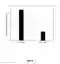
FIG. 1 provides the comparative data of wet etching rates of silicon nitride films deposited via PEALD using Monochlorosilane (MCS) and Dichlorosilane (DCS).
FIG. 2 provides the comparative data of chloride concentrations analyzed by Secondary Ion Mass Spectroscopy (SIMS) for the ALD silicon nitride films deposited at 450° C. under ammonia plasma, using Monochlorosilane (MCS) and Dichlorosilane (DCS).
DETAILED DESCRIPTION OF THE INVENTION
This invention is to address the issue of forming silicon nitride, silicon oxynitride, silicon oxide, carbon-doped silicon nitride, carbon-doped silicon oxide and carbon-doped oxynitride films at low deposition temperatures.
Dichlorosilane (DCS) has been widely used in the semiconductor industries as silicon source to deposit silicon nitride via reacting with ammonia. The typical deposition temperatures are greater than 550° C. and the by-products are two moles of HCl per DCS. The present invention uses monochlorosilane (MCS) to replace DCS to lower down the deposition temperatures as well as chloride contamination in the resulting films.
| TABLE I | |
| DE | |
| Reaction | (kcal/mol) |
| H3SiCl + NH2• → H3SiNH2 + Cl• | (1) | 6.755 |
| H3SiCl + NH2• → H2SiClNH2 + H• | (2) | −16.757 |
| H3SiCl + NH2• → H3SiNH• + HCl | (3) | 39.742 |
| H3SiCl + NH2• → H2SiClNH• + H2 | (4) | 20.208 |
| H2SiCl2 + NH2• → H2SiClNH2 + Cl• | (5) | 2.05 |
| H2SiCl2 + NH2• → HSiCl2NH2 + H• | (6) | −16.498 |
| H2SiCl2 + NH2• → H2SiClNH• + HCl | (7) | 36.801 |
| H2SiCl2 + NH2• → HSiCl2NH• + H2 | (8) | 20.445 |
| H2SiClNH2 + NH2• → H2Si(NH2)2 + Cl• | (9) | 7.222 |
| H2SiClNH2 + NH2• → HSiCl(NH2)2 + H• | (10) | −17.077 |
| H2SiClNH2 + NH2• → H2Si(NH2)(NH•) + HCl | (11) | 41.821 |
| H2SiClNH2 + NH2• → HSiCl(NH2)(NH•) + H2 | (12) | 20.178 |
| HSiCl2NH2 + NH2• → HSiCl(NH2)2 + Cl• | (13) | 1.471 |
| HSiCl2NH2 + NH2• → SiCl2(NH2)2 + H• | (14) | −19.099 |
| HSiCl2NH2 + NH2• → HSiCl(NH2)(NH•) + HCl | (15) | 36.512 |
| HSiCl2NH2 + NH2• → SiCl2(NH2)(NH•) + H2 | (16) | 18.346 |
To understand the cyclic chemical vapor deposition or atomic layer deposition processes of the reactions for DCS and monochlorosilane under ammonia plasma, quantum mechanical calculations were conducted using spin-polarized density functional theory with the PW91 exchange-correlation functional. A double numerical atomic orbital basis set augmented with polarization functions was utilized to represent the electronic structures of the molecular species. The ground state molecular structures were obtained upon full geometry optimization. The calculated thermochemical energies for various reactions of DCS or MCS with NH2. radicals generated under ammonia plasma, are shown in Table I.
From the calculated data shown in Table I, it is clear that for reactions with ammonia plasma, to thermochemically break the Si—H bonds (reactions 2, 6, 10), the chemical processes are moderately exothermic. However, to break the Si—Cl bonds via ammonia plasma, the reactions (reactions 1, 5, 9) are all endothermic. It is much easier to break the Si—H bond than the Si—Cl bond for reactions with ammonia plasma, suggesting that the NH2. radicals would react with the —SiH3 fragments anchored on the semi-fabricated substrate via reacting MCS with the surface of the substrate much easier than the —SiH2Cl fragments anchored by DCS. As a result, the ALD reaction temperatures as well as the chloride contamination can be reduced.
Working Example
Silicon Nitride Film
In this working example, a silicon oxide film has been deposited by using the following steps.
Substrates to be deposited films on were loaded to a hot wall atomic layer deposition (ALD) reactor. The reactor was flashed with Ar and pumped down to low pressure of less than 0.1 Torr (T) and heated up to a temperature at which film deposition was performed.
MCS (monochlorosilane) as the Si precursor was introduced to the reactor at a fixed flow rate. The reactor was saturated with MCS for a short fixed time (typically 10 seconds), and then pumped down to 0.1 T, followed by introducing a fixed flow of NH3. The reactor was again pumped down after NH3 precursor saturation for a short fixed time (typically 20 seconds). This cycle is repeated until desired film thickness is achieved.
The plasma power was set at approximately 100 W, and the temperature was set at approximately 450° C.
The plasma can be a nitrogen plasma, a mixture of nitrogen and hydrogen plasma, or a mixture of nitrogen and argon. The plasma can be generated in-situ plasma or remotely. The MCS can also be plasma-excited.
FIG. 1 provides the comparative data of wet etching rates of silicon nitride films deposited via PEALD. FIG. 1 shows PEALD film from Monochrosilane (MCS) is much more etching resistant than that of DCS.
FIG. 2 provides the comparative data of chloride concentrations analyzed by SIMS for the ALD silicon nitride films deposited at 450° C. under ammonia plasma. FIG. 2 suggests MCS gives lower chloride content, or lower chloride contamination.
Embodiment 1
Silicon Oxide Film
In this embodiment, a method of forming silicon oxide films comprises the following steps.
Substrates to be deposited films on are loaded to a hot wall CVD or ALD reactor. The reactor is flashed with Ar and pumped down to low pressure of less than 2 Torr (T) and heated up to a temperature at which film deposition is performed.
For CVD process, a fixed flow rate of MCS (monochlorosilane) as the Si precursor is introduced to the reactor. A fixed flow of a fixed flow of ozone as oxygen precursor is introduced to the reactor at the same time as MCS. The flow stops and then the deposition process stops when a desired film thickness is reached.
For ALD or cyclic CVD process, a fixed flow rate of MCS (monochlorosilane) as the Si precursor is introduced to the reactor. The reactor is saturated with MCS for a short fixed time (typical less than 10 seconds), and then pumped down to 2 T, followed by introducing a fixed flow of ozone, or a plasma excited O2. The reactor is again pumped down after N precursor saturation for a short fixed time (typical less than 10 seconds). This cycle is repeated until desired film thickness is achieved.
The process is preferably a plasma enhanced process, such as plasma enhanced atomic layer deposition, plasma enhanced chemical vapor deposition, and plasma enhanced cyclic chemical vapor deposition. The plasma is an in-situ generated plasma or a remotely generated plasma.
The deposition process is carried out at temperature at or below 550° C.
Embodiment 2
Silicon Oxynitride Film
In this embodiment, a method of forming silicon oxynitride films comprises the following steps.
Substrates to be deposited films on are loaded to a hot wall CVD or ALD reactor. The reactor is flashed with Ar and pumped down to low pressure of less than 2 T and heated up to a temperature at which film deposition is performed;
For CVD process, a fixed flow rate of MCS (monochlorosilane) as the Si precursor is introduced to the reactor. A fixed flow of nitrogen source such as NH3 and a fixed flow of O2 as oxygen precursor are introduced to the reactor at the same time as MCS. The flow stops and then the deposition process stops when a desired film thickness is reached.
For ALD or cyclic CVD process, a fixed flow rate of MCS (monochlorosilane) as the Si precursor is introduced to the reactor. The reactor is saturated with MCS for a short fixed time (typical less than 10 seconds), and then pumped down to 2 T, followed by introducing a fixed flow of O2 as oxygen precursor and a fixed flow of NH3. The reactor is again pumped down after N precursor saturation for a short fixed time (typical less than 10 seconds). This cycle is repeated until desired film thickness is achieved.
The process is preferably a plasma enhanced process, such as plasma enhanced atomic layer deposition, plasma enhanced chemical vapor deposition, and plasma enhanced cyclic chemical vapor deposition. The plasma is an in-situ generated plasma or a remotely generated plasma.
The deposition process is carried out at temperature at or below 550° C.
Embodiment 3
Carbon-Doped Silicon Nitride Film
In this embodiment, a method of forming carbon-doped silicon nitride films comprises the following steps.
Substrates to be deposited films on are loaded to a hot wall CVD or ALD reactor. The reactor is flashed with Ar and pumped down to low pressure of less than 2 T and heated up to a temperature at which film deposition is performed;
For CVD process, a fixed flow rate of monochloroalkylsilane having a general formula of ClSiHxR1nR2m-x wherein x=1, 2; m=1, 2, 3; n=0, 1, n+m=<3; R1 and R2 are linear, branched or cyclic independently selected from the group consisting of alkyl, alkenyl, alkynyl, aryl having 1-10 carbon atoms; as a Si precursor is introduced to the reactor. A fixed flow of nitrogen source such as NH3 is introduced to the reactor at the same time as monochloroalkylsilane. The flow stops and then the deposition process stops when a desired film thickness is reached.
The process is preferably a plasma enhanced process, such as plasma enhanced atomic layer deposition, plasma enhanced chemical vapor deposition, and plasma enhanced cyclic chemical vapor deposition. The plasma is an in-situ generated plasma or a remotely generated plasma.
For ALD or cyclic CVD process, a fixed flow rate of the Si precursor disclosed above, is introduced to the reactor. The reactor is saturated with the Si precursor for a short fixed time (typical less than 10 seconds), and then pumped down to 2 T, followed by introducing a fixed flow of NH3. The reactor is again pumped down after N precursor saturation for a short fixed time (typical less than 10 seconds). This cycle is repeated until desired film thickness is achieved.
Examples of monochloroalkylsilane are ClSiMeH2, ClSiEtH2, ClSiEt2H, ClSi(CH═CH2)H2, ClSi(CH═CH2)MeH, ClSi(CH═CH2)EtH, ClSi(CCH)H2, ClSi(iso-Pr)2H, ClSi(sec-Bu)2H, ClSi(tert-Bu)2H, ClSi(iso-Pr)H2, ClSi(sec-Bu)H2, ClSi(tert-Bu)H2.
The deposition process is carried out at temperature at or below 550° C.
Embodiment 4
Carbon-Doped Silicon Oxide Film
In this embodiment, a method of forming carbon doped silicon oxide films comprises the following steps.
Substrates to be deposited films on are loaded to a hot wall CVD or ALD reactor. The reactor is flashed with Ar and pumped down to low pressure of less than 2 T and heated up to a temperature at which film deposition is performed;
For CVD process, a fixed flow rate of monochloroalkylsilane having a general formula of ClSiHxR1nR2m-x wherein x=1, 2; m=1, 2, 3; n=0, 1, n+m=<3; R1 and R2 are linear, branched or cyclic independently selected from the group consisting of alkyl, alkenyl, alkynyl, aryl having 1-10 carbon atoms; as Si precursor is introduced to the reactor. A fixed flow of oxygen source such as ozone is introduced to the reactor at the same time as the Si precursor. The flow stops and then the deposition process stops when a desired film thickness is reached.
The process is preferably a plasma enhanced process, such as plasma enhanced atomic layer deposition, plasma enhanced chemical vapor deposition, and plasma enhanced cyclic chemical vapor deposition. The plasma is an in-situ generated plasma or a remotely generated plasma.
For ALD or cyclic CVD process, a fixed flow rate of the Si precursor disclosed above is introduced to the reactor. The reactor is saturated with the Si precursor for a short fixed time (typical less than 10 seconds), and then pumped down to 2 T, followed by introducing a fixed flow of ozone. The reactor is again pumped down after N precursor saturation for a short fixed time (typical less than 10 seconds). This cycle is repeated until desired film thickness is achieved.
Examples of monochloroalkylsilane are ClSiEtH2, ClSiEt2H, ClSi(CH═CH2)H2, ClSi(CH═CH2)MeH, ClSi(CH═CH2)EtH, ClSi(CCH)H2, ClSi(iso-Pr)2H, ClSi(sec-Bu)2H, ClSi(tert-Bu)2H, ClSi(iso-Pr)H2, ClSi(sec-Bu)H2, ClSi(tert-Bu)H2.
The deposition process is carried out at temperature at or below 550° C.
Embodiment 5
Carbon-Doped Silicon Oxynitride Film
In this embodiment, a method of forming carbon-doped silicon oxynitride films comprises the following steps.
Substrates to be deposited films on are loaded to a hot wall CVD or ALD reactor. The reactor is flashed with Ar and pumped down to low pressure of less than 2 T and heated up to a temperature at which film deposition is performed;
For CVD process, a fixed flow rate of monochloroalkylsilane having a general formula of ClSiHxR1nR2m-x wherein x=1, 2; m=1, 2, 3; n=0, 1, n+m=<3; R1 and R2 are linear, branched or cyclic independently selected from the group consisting of alkyl, alkenyl, alkynyl, aryl having 1-10 carbon atoms; as Si precursor is introduced to the reactor. A fixed flow of nitrogen source such as NH3 and a fixed flow of O2 as oxygen precursor are introduced to the reactor at the same time as the Si precursor. The flow stops and then the deposition process stops when a desired film thickness is reached.
For ALD or cyclic CVD process, a fixed flow rate of the Si precursor disclosed above is introduced to the reactor. The reactor is saturated with the Si precursor for a short fixed time (typical less than 10 seconds), and then pumped down to 2 T, followed by introducing a fixed flow of ozone. The reactor is again pumped down after N precursor saturation for a short fixed time (typical less than 10 seconds). This cycle is repeated until desired film thickness is achieved.
The process is preferably a plasma enhanced process, such as plasma enhanced atomic layer deposition, plasma enhanced chemical vapor deposition, and plasma enhanced cyclic chemical vapor deposition. The plasma is an in-situ generated plasma or a remotely generated plasma.
Examples of monochloroalkylsilane are ClSiEtH2, ClSiEt2H, ClSi(CH═CH2)H2, ClSi(CH═CH2)MeH, ClSi(CH═CH2)EtH, ClSi(CCH)H2, ClSi(iso-Pr)2H, ClSi(sec-Bu)2H, ClSi(tert-Bu)2H, ClSi(iso-Pr)H2, ClSi(sec-Bu)H2, ClSi(tert-Bu)H2.
The deposition process is carried out at temperature at or below 550° C.
The working example and embodiments of this invention listed above, are exemplary of numerous embodiments that may be made of this invention. It is contemplated that numerous other configurations of the process may be used, and the materials used in the process may be elected from numerous materials other than those specifically disclosed.
Claims
1. A process to deposit silicon nitride or carbon-doped silicon nitride on a substrate in a processing chamber, comprising:
a. contacting the substrate with a nitrogen-containing source to absorb at least a portion of the nitrogen-containing source on the substrate;
b. purging unabsorbed nitrogen-containing source;
c. contacting the substrate with a silicon-containing precursor to react with the portion of the absorbed nitrogen-containing source; and
d. purging unreacted silicon-containing source;
wherein the process is a plasma-enhanced process.
2. The process to deposit silicon nitride of claim 1 wherein the silicon-containing source is monochlorosilane.
3. The process to deposit carbon-doped silicon nitride of claim 1 wherein the silicon-containing source is monochloroalkylsilane having a general formula of ClSiHxR1nR2m-x wherein x=1, 2; m=1, 2, 3; n=0, 1, n+m=<3; R1 and R2 are linear, branched or cyclic independently selected from the group consisting of alkyl, alkenyl, alkynyl, and aryl having 1-10 carbon atoms.
4. The silicon-containing source in claim 3 is selected from the group consisting of ClSiEtH2, ClSiEt2H, ClSi(CH═CH2)H2, ClSi(CH═CH2)MeH, ClSi(CH═CH2)EtH, ClSi(CCH)H2, ClSi(iso-Pr)2H, ClSi(sec-Bu)2H, ClSi(tert-Bu)2H, ClSi(iso-Pr)H2, ClSi(sec-Bu)H2, ClSi(tert-Bu)H2, and mixtures thereof.
5. The process of claim 1 is selected from the group consisting of plasma enhanced atomic layer deposition, and plasma enhanced cyclic chemical vapor deposition; wherein the plasma is selected from the group consisting of an ammonia plasma, a nitrogen plasma, a mixture of nitrogen and hydrogen plasma, and a mixture of nitrogen and argon plasma; plasma-excited silicon precursor is optional.
6. The process of claim 5, wherein the plasma is an in-situ generated plasma or a remotely generated plasma.
7. The process of claim 1 wherein the nitrogen-containing source for depositing silicon nitride is selected from the group consisting of nitrogen, ammonia, hydrazine, monoalkylhydrozine, dialkylhydrozine, and mixture thereof; and the nitrogen-containing source for depositing carbon-doped silicon nitride is selected from the group consisting of nitrogen, ammonia, hydrazine, monoalkylhydrozine, dialkylhydrozine, hydroxylamine (NH2OH), tert-butylamine (NH2C(CH3)3), allylamine (NH2CH2CHCH2), hydroxylamine hydrochloride, methylamine, diethylamine, triethylamine and mixture thereof.
8. A process to deposit silicon oxide or carbon-doped silicon oxide on a substrate in a processing chamber, comprising:
a. contacting the substrate with an oxygen-containing source to absorb at least a portion of the oxygen-containing source on the substrate;
b. purging unabsorbed oxygen-containing source;
c. contacting the substrate with a silicon-containing precursor to react with the portion of the absorbed oxygen-containing source; and
d. purging unreacted silicon-containing source.
9. The process to deposit silicon oxide of claim 8 wherein the silicon-containing source is monochlorosilane.
10. The process to deposit carbon-doped silicon oxide of claim 8 wherein the silicon-containing source is monochloroalkylsilane having a general formula of ClSiHxR1nR2m-x wherein x=1, 2; m=1, 2, 3; n=0, 1, n+m=<3; R1 and R2 are linear, branched or cyclic independently selected from the group consisting of alkyl, alkenyl, alkynyl, and aryl having 1-10 carbon atoms.
11. The silicon-containing source in claim 10 is selected from the group consisting of ClSiEtH2, ClSiEt2H, ClSi(CH═CH2)H2, ClSi(CH═CH2)MeH, ClSi(CH═CH2)EtH, ClSi(CCH)H2, ClSi(iso-Pr)2H, ClSi(sec-Bu)2H, ClSi(tert-Bu)2H, ClSi(iso-Pr)H2, ClSi(sec-Bu)H2, ClSi(tert-Bu)H2, and mixtures thereof.
12. The process of claim 8 is selected from the group consisting of plasma enhanced atomic layer deposition, plasma enhanced chemical vapor deposition and plasma enhanced cyclic chemical vapor deposition.
13. The process of claim 12, wherein the plasma is an in-situ generated plasma or a remotely generated plasma.
14. The process of claim 8 wherein the oxygen-containing source is selected from the group consisting of oxygen, water, nitrous oxide, ozone, and mixture thereof.
15. A process to deposit silicon oxynitride or carbon-doped silicon oxynitride on a substrate in a processing chamber, comprising:
a. contacting the substrate with a mixture of an oxygen-containing source and a nitrogen-containing source to absorb at least a portion of the oxygen-containing source and at least a portion of the nitrogen-containing source on the substrate;
b. purging unabsorbed oxygen-containing source and nitrogen-containing source;
c. contacting the substrate with a silicon-containing precursor to react with the portion of the absorbed oxygen-containing source and nitrogen-containing source; and
d. purging unreacted silicon-containing source.
16. The process deposit silicon oxynitride of claim 15 wherein the silicon-containing source is monochlorosilane.
17. The process deposit carbon-doped silicon oxynitride of claim 15 wherein the silicon-containing source is monochloroalkylsilane having a general formula of ClSiHxR1nR2m-x wherein x=1, 2; m=1, 2, 3; n=0, 1, n+m=<3; R1 and R2 are linear, branched or cyclic independently selected from the group consisting of alkyl, alkenyl, alkynyl, and aryl having 1-10 carbon atoms.
18. The silicon-containing source in claim 17 is selected from the group consisting of ClSiEtH2, ClSiEt2H, ClSi(CH═CH2)H2, ClSi(CH═CH2)MeH, ClSi(CH═CH2)EtH, ClSi(CCH)H2, ClSi(iso-Pr)2H, ClSi(sec-Bu)2H, ClSi(tert-Bu)2H, ClSi(iso-Pr)H2, ClSi(sec-Bu)H2, ClSi(tert-Bu)H2, and mixtures thereof.
19. The process of claim 15 is selected from the group consisting of plasma enhanced atomic layer deposition, plasma enhanced chemical vapor deposition and plasma enhanced cyclic chemical vapor deposition.
20. The process of claim 19, wherein the plasma is an in-situ generated plasma or a remotely generated plasma.
21. The process of claim 15 wherein the oxygen-containing source is selected from the group consisting of oxygen, water, nitrous oxide, ozone, and mixture thereof.
22. The process of claim 15 wherein the nitrogen-containing source is selected from the group consisting of nitrogen, ammonia, hydrazine, monoalkylhydrozine, dialkylhydrozine, hydroxylamine (NH2OH), tert-butylamine (NH2C(CH3)3), allylamine (NH2CH2CHCH2), hydroxylamine hydrochloride, methylamine, diethylamine, triethylamine and mixture thereof.
Images & Drawings included:

Sources:
- United States Patent and Trademark Office - verify current appl. status at the USPTO↗
Similar patent applications:
- » 20120156894
Monosilane or disilane derivatives and method for low temperature deposition of silicon-containing films using the same - » 10699079
Composition and method for low temperature deposition of silicon-containing films - » 20050080285
Monosilane or disilane derivatives and method for low temperature deposition of silicon-containing films using the same - » 10294431
Composition and method for low temperature deposition of silicon-containing films such as films including silicon nitride, silicon dioxide and/or silicon-oxynitride - » 20080160174
Monosilane or disilane derivatives and method for low temperature deposition of silicon-containing films using the same - » 20090084288
Composition and method for low temperature deposition of silicon-containing films - » 20090281344
Composition and method for low temperature deposition of silicon-containing films such as films including silicon, silicon nitride, silicon dioxide and/or silicon-oxynitride - » 20130189853
Low temperature deposition of silicon-containing films - » 20100221914
Composition and method for low temperature deposition of silicon-containing films - » 20100285663
Composition and method for low temperature deposition of silicon-containing films such as films including silicon, silicon nitride, silicon dioxide and/or silicon-oxynitride
Recent applications in this class:
- » 20250239445 2025-07-24
METHOD AND APPARATUS FOR SELECTIVE DEPOSITION OF DIELECTRIC FILMS - » 20250174456 2025-05-29
THERMAL CVD OF TITANIUM SILICIDE METHODS TO FORM SEMICONDUCTOR STRUCTURES - » 20250095984 2025-03-20
IN-SITU SIDEWALL PASSIVATION TOWARD THE BOTTOM OF HIGH ASPECT RATIO FEATURES - » 20250029830 2025-01-23
VAPOR PHASE TRANSPORT SYSTEM AND METHOD FOR DEPOSITING PEROVSKITE SEMICONDUCTORS - » 20250014894 2025-01-09
Substrate Processing Method, Method of Manufacturing Semiconductor Device, Substrate Processing Apparatus and Non-transitory Computer-readable Recording Medium - » 20240371630 2024-11-07
SEMICONDUCTOR DEVICE STRUCTURE AND MANUFACTURING METHOD THEREOF - » 20240266164 2024-08-08
METHOD OF PROCESSING SUBSTRATE, METHOD OF MANUFACTURING SEMICONDUCTOR DEVICE, RECORDING MEDIUM, AND SUBSTRATE PROCESSING APPARATUS - » 20240222109 2024-07-04
SUBSTRATE PROCESSING APPARATUS, METHOD OF MANUFACTURING SEMICONDUCTOR DEVICE, AND RECORDING MEDIUM - » 20240105445 2024-03-28
FILM FORMING METHOD AND SUBSTRATE PROCESSING SYSTEM - » 20240096615 2024-03-21
SUBSTRATE PROCESSING APPARATUS, PROCESSING METHOD, AND NON-TRANSITORY COMPUTER-READABLE RECORDING MEDIUM
Recent applications for this Assignee:
- » 20250293095 2025-09-18
SYSTEM AND METHOD OF PULSE SCORING - » 20250293065 2025-09-18
BONDING APPARATUS AND BONDING METHOD - » 20250293058 2025-09-18
SEPARATING APPARATUS AND SEPARATING METHOD - » 20250293042 2025-09-18
HARC ETCH CHEMISTRY FOR SEMINCONDUCTORS - » 20250293010 2025-09-18
SUBSTRATE PROCESSING APPARATUS, SUBSTRATE PROCESSING SYSTEM, AND MAINTENANCE METHOD - » 20250293005 2025-09-18
PLASMA PROCESSING APPARATUS - » 20250292996 2025-09-18
PLASMA PROCESSING APPARATUS - » 20250292374 2025-09-18
METHOD OF GENERATING LEARNING MODEL, INFORMATION PROCESSING METHOD, RECORDING MEDIUM, AND INFORMATION PROCESSING DEVICE - » 20250292119 2025-09-18
RECORDING MEDIUM, INFORMATION PROCESSING APPARATUS, AND INFORMATION PROCESSING METHOD - » 20250291849 2025-09-18
RECORDING MEDIUM, INFORMATION PROCESSING APPARATUS, AND INFORMATION PROCESSING METHOD