Harmonic suppression device
US20110032052A1
2011-02-10
12/603,654
2009-10-22
✅ Patent granted
US 8,217,735 B2
2012-07-10
-
-
Barbara Summons
2030-10-30
Abstract:
A harmonic suppression device includes a multilayer printed circuit board (PCB). The multilayer PCB includes a first layer, a second layer, and a third layer. The third layer is connected to the ground. The first layer is configured with a power amplifier, an input microstrip, a voltage divider microstrip, and an output microstrip. The power amplifier is operable to amplify radio frequency (RF) signals input using the input microstrip and to output the amplified RF signals using the output microstrip. The second layer is configured with a first microstrip and a second microstrip. One end of each of the first and second microstrips is connected to an alternative one of the first layer and the third layer by vias, and the other ends of the first and second microstrips are unattached so as to suppress harmonics on the power amplifier.
Inventors:
- SHYUE-DAR CHEN 2 🇹🇼 Tu-Cheng, Taiwan
- CHIH-MING HUNG 1 🇹🇼 Tu-Cheng, Taiwan
- Shyue-Dar Chen 2 🇹🇼 Taipei Hsien, Taiwan
- Chih-Ming Hung 1 🇹🇼 Taipei Hsien, Taiwan
Assignee:
- HON HAI PRECISION INDUSTRY CO., LTD. 12,833 🇹🇼 Tu-Cheng, Taiwan
- HON HAI PRECISION INDUSTRY CO., LTD. 2,724 🇹🇼 Tu-Cheng, New Taipei, Taiwan
Interested in similar patents?
Get notified when new applications in this technology area are published.
Classification:
H01P1/20345 » CPC main
Auxiliary devices; Frequency-selective devices, e.g. filters; Filters for transverse electromagnetic waves; Strip line filters; Electromagnetic interstage coupling; Comb or interdigital filters Multilayer filters
H03F1/32 » CPC further
Details of amplifiers with only discharge tubes, only semiconductor devices or only unspecified devices as amplifying elements Modifications of amplifiers to reduce non-linear distortion
H03F3/60 » CPC further
Amplifiers with only discharge tubes or only semiconductor devices as amplifying elements Amplifiers in which coupling networks have distributed constants, e.g. with waveguide resonators
H03H7/01 IPC
Multiple-port networks comprising only passive electrical elements as network components Frequency selective two-port networks
H03H7/00 IPC
Multiple-port networks comprising only passive electrical elements as network components
H03F3/213 IPC
Amplifiers with only discharge tubes or only semiconductor devices as amplifying elements; Power amplifiers, e.g. Class B amplifiers, Class C amplifiers with semiconductor devices only in integrated circuits
H04B1/04 IPC
Details of transmission systems, not covered by a single one of groups - ; Details of transmission systems not characterised by the medium used for transmission; Transmitters Circuits
Description
BACKGROUND
1. Technical Field
Embodiments of the present disclosure relate to wireless communication, and more particularly to a harmonic suppression device utilized thereby.
2. Description of Related Art
Wireless communication protocols usually require noise generated by wireless terminals to be below a set value. Because of nonlinearity of power amplifiers and other elements in those wireless terminals radiating from high power loads, harmonics of transmission signals generate high noise, such as quadric harmonics and third harmonics, easily exceeding the desired limit. Suppression of harmonics to linearize output of the power amplifiers is thus critical.
Currently, most attempts at suppression apply patched low pass filters after the power amplifiers to filter the harmonics. However, the patched low pass filters incorporate a plurality of elements, increasing cost and size of the wireless terminals. In addition, loss, inherent in most patched low pass filters reduces output power and increases wasted power. Therefore, a heretofore unaddressed need exists to address the limitations described.
BRIEF DESCRIPTION OF THE DRAWINGS
The details of the disclosure, both as to its structure and operation, can best be understood by referring to the accompanying drawings, in which like reference numbers and designations refer to like elements.
FIG. 1 is a schematic diagram of one embodiment of three layers of a harmonic suppression device of the present disclosure;
FIG. 2 is a schematic diagram of one embodiment of a harmonic suppression device of the present disclosure;
FIG. 3 is a schematic diagram of another embodiment of a harmonic suppression device of the present disclosure;
FIG. 4 is a schematic diagram of another embodiment of a harmonic suppression device of the present disclosure; and
FIG. 5 is a schematic diagram of another embodiment of a harmonic suppression device of the present disclosure.
DETAILED DESCRIPTION
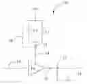
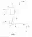
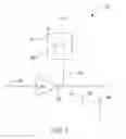
FIG. 1 is a schematic diagram of one embodiment of three layers of a harmonic suppression device 10 of the present disclosure. FIG. 2 is a schematic diagram of one embodiment of a harmonic suppression device 10 of the present disclosure.
The harmonic suppression device 10 includes a multilayer printed circuit board (PCB). In one embodiment, the multilayer PCB includes a first layer 100, a second layer 200, and a third layer 300. The third layer 300 is connected to ground.
The first layer 100 is configured with a power amplifier PA, an input microstrip 13, a voltage divider microstrip 14, and an output microstrip 15. The harmonic suppression device 10 is used to improve linearity of the power amplifier PA. The power amplifier PA is operable to amplify radio frequency (RF) signals input using the input microstrip 13 and to output the amplified RF signals using the output microstrip 15. The voltage divider microstrip 14 is operable to transmit an external voltage Vcc to the power amplifier PA. In one embodiment, the voltage divider microstrip 14 and the output microstrip 15 are connected to different pins of the power amplifier PA.
In one embodiment, the first layer 100 is further configured with a capacitor C1 and an inductor L1. The capacitor C1 and the inductor L1 are connected in parallel and subsequently connected to the voltage divider microstrip 14, to transmit the external voltage Vcc to the power amplifier PA.
The second layer 200 is configured with a first microstrip 16 and a second microstrip 17 to improve linearity of the power amplifier PA. One end of each of the first and second microstrips 16, 17 is connected to the first layer 100 by vias. The other ends of each of the first and second microstrips 16, 17 are unattached so as to suppress harmonics on the power amplifier PA.
In one embodiment, the PCB defines a first via 11 and a second via 12 through the first layer 100 to the second layer 200. In the first layer 100, the first via 11 is defined in the voltage divider microstrip 14 and the second via 12 is defined in the output microstrip 15.
As such, one end of the first microstrip 16 is connected to the voltage divider microstrip 14 of the first layer 100 by the first via 11 and another end of the first microstrip 16 is unattached. One end of the second microstrip 17 is connected to the output microstrip 15 of the first layer 100 using the second via 12 and another end of the second microstrip 17 is unattached. In one embodiment, the first and second microstrips 16, 17 are both a quarter wavelength of the RF signal received by the power amplifier PA in length.
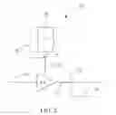
FIG. 2 is a schematic diagram of another embodiment of a harmonic suppression device 20 of the present disclosure, differing from the harmonic suppression device 10 of FIG. 1 in that the voltage divider microstrip 24 and the output microstrip 25 are connected to one and the same pin of the power amplifier PA. The output microstrip 25 is connected to the second microstrip 27 on the second layer 200 using a capacitor C2.
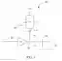
FIG. 3 is a schematic diagram of another embodiment of a harmonic suppression device of the present disclosure, differing from the harmonic suppression device 10 of FIG. 1 in that one end of each of the first and second microstrips 36, 37 is connected to the third layer 300 by vias.
In one embodiment, the PCB defines a third via 31 and a fourth via 32 through the second layer 200 to the third layer 300. In detail, one end of the first microstrip 36 is connected to the third layer 300 and then to the ground using the third via 31, and another end of the first microstrip 36 is unattached. One end of the second microstrip 37 is connected to the third layer 300 and then to the ground using the fourth via 32, and another end of the second microstrip 37 is unattached.
FIG. 4 is a schematic diagram of another embodiment of a harmonic suppression device of the present disclosure, differing from the harmonic suppression device 30 of FIG. 3 in that the voltage divider microstrip 44 and the output microstrip 45 are connected to one and the same pin of the power amplifier PA. The output microstrip 45 outputs the RF signals using a capacitor C2.
As such, one end of each of the first and second microstrips is connected to an alternative one of the first layer 100 and the third layer 300 by vias. The other ends of the first and second microstrips are unattached to suppress harmonics on the power amplifier PA. Therefore, embodiments of the harmonic suppression devices of the present disclosure suppress the harmonic of the power amplifier PA by the multilayer PCB, which improves linearity of the power amplifier PA and then linearizes the output of the power amplifier PA.
In addition, embodiments of the harmonic suppression devices of the present disclosure are all implemented by PCB, which reduces cost, element number, and size of wireless terminals. Furthermore, the PCB is much more reliable than patched elements. Therefore, embodiments of the harmonic suppression devices of the present disclosure have fewer elements but higher reliability.
While various embodiments and methods of the present disclosure have been described above, it should be understood that they have been presented using example only and not using limitation. Thus the breadth and scope of the present disclosure should not be limited by the above-described embodiments, but should be defined only in accordance with the following claims and their equivalents.
Claims
What is claimed is:1. A harmonic suppression device comprising a multilayer printed circuit board (PCB), wherein the multilayer PCB comprises:
a first layer configured with a power amplifier, an input microstrip, a voltage divider microstrip, and an output microstrip, wherein the power amplifier is operable to amplify radio frequency (RF) signals input using the input microstrip and to output the amplified RF signals using the output microstrip, and the voltage divider microstrip is operable to transmit an external voltage to the power amplifier;
a second layer configured with a first microstrip and a second microstrip, the first microstrip and the second microstrip operable to improve linearity of the power amplifier; and
a third layer connected to ground;
wherein one end of each of the first and second microstrips is connected to an alternative one of the first layer and the third layer by vias, and the other ends of the first and second microstrips are unattached to suppress harmonics on the power amplifier.
2. The harmonic suppression device as claimed in claim 1, wherein one end of the first microstrip is connected to the voltage divider microstrip on the first layer.
3. The harmonic suppression device as claimed in claim 2, wherein one end of the second microstrip is connected to the output microstrip on the first layer.
4. The harmonic suppression device as claimed in claim 1, wherein the first and second microstrips are both connected to the third layer.
5. The harmonic suppression device as claimed in claim 1, wherein the first and second microstrips are both a quarter of the wavelength of the RF signal received by the power amplifier in length.
6. The harmonic suppression device as claimed in claim 1, wherein the first layer is further configured with a capacitor and an inductor connected in parallel, and subsequently connected to the voltage divider microstrip to transmit the external voltage to the power amplifier.
Images & Drawings included:
Sources:
- United States Patent and Trademark Office - verify current appl. status at the USPTO↗
Similar patent applications:
- » 20200067399
Harmonic suppression device and harmonic suppression system - » 20200006939
Electric motor system and high-frequency harmonic suppressing device of the same - » 20250185135
LIGHTING DEVICE HAVING HARMONIC SUPPRESSING FUNCTION - » 20130135907
Harmonic current suppression method and harmonic current suppression device of power conversion device - » 20150341126
Method and device for suppressing harmonic signals - » 20190326753
PHOTOVOLTAIC POWER GENERATION SYSTEM AND METHOD AND DEVICE FOR SUPPRESSING HARMONIC WAVE - » 20230318569
Radio-frequency circuits and devices having harmonic suppression - » 20200373828
Device and method for suppressing harmonic distortions at the output of variable frequency drive - » 20220014114
Power conversion device capable of suppressing a harmonic component in an output voltage from an arm that increases after bypass of a failed converter cell - » 18630251
Active power filtering-based harmonic suppression method, system and device using VOC inverter
Recent applications in this class:
- » 20240387969 2024-11-21
FILTER - » 20240304970 2024-09-12
MULTILAYERED FILTER DEVICE - » 20230223671 2023-07-13
MULTI-LAYER WAVEGUIDE WITH METASURFACE, ARRANGEMENT, AND METHOD FOR PRODUCTION THEREOF - » 20230216165 2023-07-06
FILTER DEVICE - » 20230127771 2023-04-27
Multilayered filter device - » 20230057594 2023-02-23
A ROLLED OR FOLDED FILTER - » 20220006170 2022-01-06
Filter - » 20210328317 2021-10-21
Multilayered filter device - » 20210305669 2021-09-30
Filter - » 20200203794 2020-06-25
LOW TEMPERATURE CO-FIRED CERAMIC FILTER
Recent applications for this Assignee:
- » 20140233961 2014-08-21
Optical communication module including optical-electrical signal converters and optical signal generators - » 20140083669 2014-03-27
HEAT SINK - » 20140063746 2014-03-06
Electronic device with heat dissipation assembly - » 20140061224 2014-03-06
AUTOMATIC VENDING MACHINE - » 20140060914 2014-03-06
Enclosure with shield apparatus - » 20140058727 2014-02-27
MULTIMEDIA RECORDING SYSTEM AND METHOD - » 20140055955 2014-02-27
Fastener - » 20140055322 2014-02-27
DISPLAY SYSTEM AND HEAD-MOUNTED DISPLAY APPARATUS - » 20140054439 2014-02-27
CONTAINER DATA CENTER WITH SUPPORTING APPARATUS - » 20140054311 2014-02-27
AUTOMATIC VENDING MACHINE WITH MOVING MEMBER FOR PRODUCTS