Stacked multi-chip
US20120007251A1
2012-01-12
12/882,805
2010-09-15
✅ Patent granted
US 8,174,126 B2
2012-05-08
-
-
Chris Chu
2031-01-20
Abstract:
A stacked multi-chip comprises a base layer, a first chip, a first stacked chip and at least one second stacked chip. The base layer comprises a mounting panel and a redistributed layer. The redistributed layer is mounted on the mounting panel. The first chip comprises an electrically non-conductive layer and a connective layer. The electrically non-conductive layer comprises a TSV channel. The connective layer abuts the redistributed layer. The first stacked chip is mounted on the first chip and comprises an electrically non-conductive layer and a connective layer. The electrically non-conductive layer comprises a TSV channel that is connected to the TSV channel of the first chip. The second stacked chip is mounted on the first stacked chip and comprises an electrically non-conductive layer and a connective layer. The electrically non-conductive layer comprises a TSV channel. The connective layer is connected to the connective layer of the first stacked chip.
Inventors:
- Ting-Ting Hwang 3 🇹🇼 Hsinchu, Taiwan
- Chen Hsien-Te 1 🇹🇼 Hsinchu, Taiwan
- Hsien-Te Chen 1 🇹🇼 Hsinchu, Taiwan
Assignee:
- NATIONAL TSING HUA UNIVERSITY 1,388 🇹🇼 Hsinchu, Taiwan
Interested in similar patents?
Get notified when new applications in this technology area are published.
Classification:
H01L2924/0002 » CPC further
Indexing scheme for arrangements or methods for connecting or disconnecting semiconductor or solid-state bodies as covered by; Technical content checked by a classifier Not covered by any one of groups , and
H01L2924/00 » CPC further
Indexing scheme for arrangements or methods for connecting or disconnecting semiconductor or solid-state bodies as covered by
H01L23/5286 » CPC main
Details of semiconductor or other solid state devices; Arrangements for conducting electric current within the device in operation from one component to another, i.e. interconnections, e.g. wires, lead frames including external interconnections consisting of a multilayer structure of conductive and insulating layers inseparably formed on the semiconductor body layout of the interconnection structure Arrangements of power or ground buses
H01L23/481 » CPC further
Details of semiconductor or other solid state devices; Arrangements for conducting electric current to or from the solid state body in operation, e.g. leads, terminal arrangements ; Selection of materials therefor Internal lead connections, e.g. via connections, feedthrough structures
H01L25/0657 » CPC further
Assemblies consisting of a plurality of individual semiconductor or other solid state devices ; Multistep manufacturing processes thereof all the devices being of a type provided for in the same subgroup of groups - , e.g. assemblies of rectifier diodes the devices not having separate containers the devices being of a type provided for in group Stacked arrangements of devices
H01L2223/6616 » CPC further
Details relating to semiconductor or other solid state devices covered by the group; Structural electrical arrangements for semiconductor devices not otherwise provided for; Impedance arrangements; High-frequency adaptations; High-frequency electrical connections Vertical connections, e.g. vias
H01L2223/6666 » CPC further
Details relating to semiconductor or other solid state devices covered by the group; Structural electrical arrangements for semiconductor devices not otherwise provided for; Impedance arrangements; High-frequency adaptations for passive devices for decoupling, e.g. bypass capacitors
H01L2225/06513 » CPC further
Details relating to assemblies covered by the group but not provided for in its subgroups; All the devices being of a type provided for in the same subgroup of groups - the devices not having separate containers the devices being of a type provided for in group; Stacked arrangements of devices Bump or bump-like direct electrical connections between devices, e.g. flip-chip connection, solder bumps
H01L2225/06544 » CPC further
Details relating to assemblies covered by the group but not provided for in its subgroups; All the devices being of a type provided for in the same subgroup of groups - the devices not having separate containers the devices being of a type provided for in group; Stacked arrangements of devices; Conductive via connections through the device, e.g. vertical interconnects, through silicon via [TSV] Design considerations for via connections, e.g. geometry or layout
H01L23/12 IPC
Details of semiconductor or other solid state devices Mountings, e.g. non-detachable insulating substrates
H01L23/52 IPC
Details of semiconductor or other solid state devices Arrangements for conducting electric current within the device in operation from one component to another, i.e. interconnections, e.g. wires, lead frames
H01L23/48 IPC
Details of semiconductor or other solid state devices Arrangements for conducting electric current to or from the solid state body in operation, e.g. leads, terminal arrangements ; Selection of materials therefor
Description
FIELD OF THE INVENTION
The present invention is a stacked multi-chip.
BACKGROUND OF THE INVENTION
In high-density electrical interconnections, a conventional stacked multi-chip achieves better performance in speed and power by using Through Silicon Via (TSV) technology to stack several chips and give the stacked multi-chip high performance, high density and smaller dimensions. For example, U.S. Pat. No. 7,091,592 B2 discloses a semiconductor chip that uses TSV in a stacked multi-chip.
However, the conventional stacked multi-chip that uses TSV technology has three problems: inadequate thermal dissipation, difficulty to constructing fully-stacked TSV for all chips and difficulty of placing voltage level shifters.
Accordingly, what is needed in the art is a new design of the stacked multi-chip that uses TSV technology to have good thermal dissipation, be easy to construct fully-stacked TSV for all chips and be easy to position voltage level shifters.
SUMMARY OF THE INVENTION
The objective of the present invention is to provide a stacked multi-level chip that has good thermal dissipation, is easy to construct fully-stacked TSV for all chips and is easy to position voltage level shifters.
The stacked multi-chip in accordance with the present invention comprises a base layer, a first chip, a first stacked chip and at least one second stacked chip. The base layer comprises a mounting panel and a redistributed layer. The redistributed layer is mounted on the mounting panel.
The first chip comprises an electrically non-conductive layer and a connective layer. The electrically non-conductive layer comprises a TSV channel. The connective layer abuts the redistributed layer.
The first stacked chip is mounted on the first chip and comprises an electrically non-conductive layer and a connective layer. The electrically non-conductive layer comprises a TSV channel that is connected to the TSV channel of the first chip.
The second stacked chip is mounted on the first stacked chip and comprises an electrically non-conductive layer and a connective layer. The electrically non-conductive layer comprises a TSV channel. The connective layer is connected to the connective layer of the first stacked chip.
BRIEF DESCRIPTION OF THE DRAWINGS
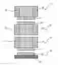
FIG. 1 is a front cross sectional view of a stacked multi-chip in accordance with the present invention;
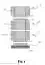
FIG. 2 is a perspective view of electrical-connections in the stacked multi-chip in FIG. 1; and
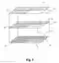
FIG. 3 is a perspective view of voltage zones of the stacked multi-chip in FIG. 1.
DETAILED DESCRIPTION OF THE PRESENT INVENTION
With reference to FIG. 1, a stacked multi-chip in accordance with the present invention has good thermal dissipation, is easy to construct fully-stacked TSV for all chips, allows voltage level shifters to be easily positioned and comprises a base layer (10), a first chip (11), a first stacked chip (12) and at least one second stacked chip (13).
The base layer (10) comprises a mounting panel (101) and a redistributed layer (102). The mounting panel (101) is non-conductive and has an outer surface and an inner surface. The outer surface is mounted in an electrical device. The redistributed layer (102) is mounted on the inner surface of the mounting panel (101), has a top surface and may use metal wire mounted on the top surface.
With further reference to FIGS. 2 and 3, the first chip (11) comprises an electrically non-conductive layer (110) and a connective layer (111). The electrically non-conductive layer (110) has a top surface and a bottom surface, may be silicon and comprises a Through Silicon Via (TSV) channel (112). The TSV channel (112) is a good thermal conductor, may have multiple voltage zones and electrical-connections, may be a hole in the electrically non-conductive layer (110) formed by TSV technology and has multiple vias formed through the channel with metal as conductors to form a decoupling capacitor that filters harmonic waves and reduces noise. The connective layer (111) is mounted against the bottom surface of the electrically non-conductive layer (110) and the TSV channel (112), abuts the redistributed layer (102) and may comprise multiple electrically and thermally conductive sections. The electrically and thermally conductive sections may be isolated from each other and may correspond respectively to the voltage zones of the TSV channel (112).
The first stacked chip (12) is mounted on the first chip (11) and comprises an electrically non-conductive layer (120) and a connective layer (121). The electrically non-conductive layer (120) has a top surface and a bottom surface, may be silicon and comprises a TSV channel (122). The TSV channel (122) corresponds and connects to the TSV channel (112) of the first chip (11), may be a hole in the electrically non-conductive layer (120) formed by TSV technology, has multiple vias and metal in the vias as conductors to form a decoupling capacitor that filters harmonic waves and reduces noise, is a good thermal conductor and may have multiple voltage zones and electrical-connections. The voltage zones of the TSV channel (122) may correspond respectively to the voltage zones of the TSV channel (112) of the first chip (11), which would make implementing voltage level shifters easy. For example, each voltage zone on the TSV channel (122) of the first stacked chip (12) may correspond to three voltage zones (30, 31, 32) on the TSV channel (112) of the first chip (11). The electrical connections of the TSV channel (122) may be proportional to the electrical connections of the TSV channel (112) of the first chip (11). The connective layer (121) is mounted against the top surface of the electrically non-conductive layer (120) and the TSV channel (122) and may comprise multiple electrically and thermally conductive sections. The electrically and thermally conductive sections may be isolated from each other and may correspond to the voltage zones of the TSV channel (122) in the first stacked chip (12).
The at least one second stacked chip (13) is mounted on the first stacked chip (12) and comprises an electrically non-conductive layer (130) and a connective layer (131). The electrically non-conductive layer (130) has a top surface and a bottom surface, may be silicon and comprises a TSV channel (132). The TSV channel (132) may be a hole in the electrically non-conductive layer (130), is formed by TSV technology with multiple vias and metal in the vias as conductors to form a decoupling capacitor that filters harmonic waves and reduces noise, is a good thermal conductor and may have multiple voltage zones and electrical-connections. The voltage zones of the TSV channel (132) may correspond to the voltage zones of the TSV channel (122) of the first stacked chip (12), which would make implementing voltage level shifters easy. For example, each voltage zone on the TSV channel (132) of the second stacked chip (13) may correspond to three voltage zones (30, 31, 32) on the TSV channel (122) of the first stacked chip (12). The electrical-connections of the TSV channel (132) may be proportional to the electrical-connections of the TSV channel (122) of the first stacked chip (12). The electrical connections may have a proportional relationship of 4:2:1. The connective layer (131) is mounted against the bottom surface of the electrically non-conductive layer (130) and the TSV channel (132), is connected to the connective layer (121) and may comprise multiple electrically and thermally conductive sections. The electrically and thermally conductive sections may be isolated from each other and may correspond respectively to the voltage zones of the TSV channel (132).
Various changes can be made without departing from the broad spirit and scope of the invention.
Claims
What is claimed is:1. A stacked multi-chip comprising
a base layer comprising
a mounting panel being non-conductive and having
an outer surface being mounted in an electrical device; and
an inner surface; and
a redistributed layer being mounted on the inner surface of the mounting panel and having a top surface;
a first chip comprising
an electrically non-conductive layer having a top surface and a bottom surface and comprising a Through Silicon Via (TSV) channel being a good thermal conductor and having multiple vias formed through the channel with metal as conductors to form a decoupling capacitor that filters harmonic waves and reduces noise; and
a connective layer being mounted against the bottom surface of the electrically non-conductive layer and the TSV channel and abutting the redistributed layer; and
a first stacked chip being mounted on the first chip and comprising
an electrically non-conductive layer having a top surface and a bottom surface and comprising a TSV channel being a good thermal conductor, corresponding and being connected to the TSV channel of the first chip and having multiple vias and metal in the vias as conductors to form a decoupling capacitor that filters harmonic waves and reduces noise; and
a connective layer being mounted against the top surface of the electrically non-conductive layer and the TSV channel of the first stacked chip; and
at least one second stacked chip being mounted on the first stacked chip and comprising
an electrically non-conductive layer having a top surface and a bottom surface and comprising a TSV channel being formed by TSV technology with multiple vias and metal in the vias as conductors to form a decoupling capacitor and being a good thermal conductor; and
a connective layer being mounted against the bottom surface of the electrically non-conductive layer and the TSV channel of the second stacked chip and being connected to the connective layer of the first stacked chip.
2. The stacked multi-chip as claimed in claim 1, wherein the redistributed layer uses metal wire mounted on the top surface.
3. The stacked multi-chip as claimed in claim 1, wherein
the electrically non-conductive layer of the first chip is silicon;
the electrically non-conductive layer of the first stacked chip is silicon; and
the electrically non-conductive layer of the second stacked chip is silicon.
4. The stacked multi-chip as claimed in claim 1, wherein
the TSV channel of the first stacked chip corresponds and connects to the TSV channel of the first chip; and
the TSV channel of the second stacked chip corresponds and connects to the TSV channel of the first stacked chip.
5. The stacked multi-chip as claimed in claim 1, wherein
the TSV channel of the first chip is a hole formed in the electrically non-conductive layer formed by TSV technology and has multiple vias formed through the channel with metal as conductors to form a decoupling capacitor;
the TSV channel of the first stacked chip is a hole formed in the electrically non-conductive layer formed by TSV technology and has multiple vias formed through the channel with metal as conductors to form a decoupling capacitor; and
the TSV channel of the second stacked chip is a hole formed in the electrically non-conductive layer by TSV technology and has multiple vias formed through the channel with metal in the vias as conductors to form a decoupling capacitor.
6. The stacked multi-chip as claimed in claim 1, wherein
the TSV channel of the first chip has multiple voltage zones;
the TSV channel of the first stacked chip has multiple voltage zones that correspond respectively to the voltage zones of the first chip; and
the TSV channel of the second stacked chip has multiple voltage zones that correspond respectively to the voltage zones of the first stacked chip.
7. The stacked multi-chip as claimed in claim 6, wherein the connective layer of the first chip comprises
multiple electrically and thermally conductive sections being isolated from each other and corresponding respectively to the voltage zones of the TSV channel of the first chip.
8. The stacked multi-chip as claimed in claim 6, wherein the connective layer of the first stacked chip comprises
multiple electrically and thermally conductive sections being isolated from each other and corresponding respectively to the voltage zones of the TSV channel of the first stacked chip.
9. The stacked multi-chip as claimed in claim 6, wherein the connective layer of the second stacked chip comprises
multiple electrically and thermally conductive sections being isolated from each other and corresponding respectively to the voltage zones of the TSV channel of the second stacked chip.
10. The stacked multi-chip as claimed in claim 1, wherein
the TSV channel of the first chip has multiple electrical-connections;
the TSV channel of the first stacked chip has multiple electrical-connections proportional to the multiple electrical-connections in the TSV channel of first chip; and
the TSV channel of the second stacked chip has multiple electrical connections proportional to the multiple electrical-connections in the TSV channel of first stacked chip.
11. The stacked multi-chip as claimed in claim 10, wherein the electrical connections are in a proportional relationship of 4:2:1.
Images & Drawings included:

Sources:
- United States Patent and Trademark Office - verify current appl. status at the USPTO↗
Similar patent applications:
- » 20080265389
Substrate for multi-chip stacking, multi-chip stack package utilizing the substrate and its applications - » 20050285250
Stacked multi-chip semiconductor package improving connection reliability of stacked chips - » 20060057773
Method for producing a stack of chips, a stack of chips and method for producing a chip for a multi-chip stack - » 10697111
Multi-chip stack flip-chip package - » 10747127
Multi-chips stacked package - » 10747128
Multi-chips stacked package - » 10620721
Low profile stacked multi-chip package and method of forming same - » 13042136
Multi-chip stacking method to reduce voids between stacked chips - » 10747114
Multi-chips stacked package - » 10820826
Multi-chips stacked package
Recent applications in this class:
- » 20250293161 2025-09-18
SEMICONDUCTOR DEVICE WITH SOURCE/DRAIN CONTACT MOL CUT STRUCTURE - » 20250285976 2025-09-11
POWER RAIL CAP FOR DEVICES WITH BACKSIDE METALLIZATION - » 20250285975 2025-09-11
ENHANCED POWER RAIL CONNECTION - » 20250285974 2025-09-11
SELF-ALIGNED BACKSIDE VIA FOR BACKSIDE POWER SCHEME - » 20250285973 2025-09-11
SOURCE/DRAIN CONTACT CUT AND POWER RAIL NOTCH - » 20250273571 2025-08-28
BACKSIDE CONTACT FORMATION FOR A SEMICONDUCTOR DEVICE STRUCTURE WITH A DENSE GATE PITCH - » 20250266355 2025-08-21
SEMICONDUCTOR DEVICE INCLUDING SWITCH CELL COUPLED TO BACKSIDE GLOBAL POWER RAIL - » 20250259930 2025-08-14
INTEGRATED CIRCUIT DEVICE AND METHOD - » 20250259929 2025-08-14
SEMICONDUCTOR DEVICE AND METHOD OF MANUFACTURING THE SAME - » 20250253243 2025-08-07
INTEGRATED CIRCUIT AND METHOD FOR FORMING THE SAME
Recent applications for this Assignee:
- » 20250175185 2025-05-29
SUCCESSIVE APPROXIMATION ANALOG-TO-DIGITAL CONVERTER FOR A PAM-(2N-2) RECEIVER - » 20250142264 2025-05-01
PIEZOELECTRIC SPEAKER AND METHOD FOR MANUFACTURING THE SAME - » 20250142263 2025-05-01
PIEZOELECTRIC SPEAKER AND METHOD FOR MANUFACTURING THE SAME - » 20250114638 2025-04-10
RADIOTHERAPY SYSTEM, METHOD FOR DELIVERING NEUTRON ACCEPTOR, AND METHOD FOR TREATING OR DIAGNOSING CANCER - » 20250054459 2025-02-13
EMOTION PERCEIVING ARTIFICIAL INTELLIGENCE MASK AND OPERATING METHOD - » 20250007758 2025-01-02
FEED-FORWARD EQUALIZER - » 20240404611 2024-12-05
ONE-TIME-PROGRAMMABLE MEMORY DEVICES - » 20240404511 2024-12-05
METHOD AND SYSTEM FOR FAIR SPEECH EMOTION RECOGNITION - » 20240402011 2024-12-05
TWO-DIMENSIONAL HYPERSPECTRAL IMAGING SYSTEM AND METHOD THEREOF - » 20240372561 2024-11-07
Decoder for decoding data in a PAM-2M format, decoder device using the decoder, and receiver using the decoder device