Method for removing polymer after etching gate stack structure of high-K gate dielectric/metal gate
US20120115321A1
2012-05-10
13/130,514
2011-02-15
✅ Patent granted
US 8,334,205 B2
2012-12-18
WO; PCT/CN2011/070996; 20110215
WO; WO2012/062059; 20120518
Cheung Lee
2031-02-15
Abstract:
The present invention provides a method for removing polymer after etching a gate stack structure of high-K gate dielectric/metal gate. The method mainly comprises the following steps: 1): forming a gate stack structure of interface SiO2/high-K gate dielectric/metal gate/poly-silicon/hard mask in sequence on a silicon substrate with device isolations formed thereon; 2): forming a resist pattern by the lithography; 3): etching the gate stack structure; and 4): immersing the resultant structure of the step 3) in an etching solution to remove the polymer, wherein the etching solution consists of HF, HCl and water, the ratio of HF by volume is 0.2˜1% and the ratio of HCl by volume is 5˜15%. According to the present invention, the wet chemical etching using a mixed solution of HF and HCl is adopted and thus it is possible to completely remove the polymer remained on both sides of the gate stack and on the surface of the silicon substrate under the room temperature. According to the present invention, it is possible not only to keep a vertical etched profile of the gate stack, but also to cause no damage on the silicon substrate. The method is well compatible with the CMOS processes and is cost efficient.
Assignee:
- Institute of Microelectronics. Chinese Academy of Sciences 521 🇨🇳 Beijing, China
Interested in similar patents?
Get notified when new applications in this technology area are published.
Classification:
H01L21/02071 » CPC main
Processes or apparatus adapted for the manufacture or treatment of semiconductor or solid state devices or of parts thereof; Manufacture or treatment of semiconductor devices or of parts thereof; Cleaning; Cleaning during device manufacture during, before or after processing of conductive layers, e.g. polysilicon or amorphous silicon layers the processing being a delineation, e.g. RIE, of conductive layers
H01L21/28017 » CPC further
Processes or apparatus adapted for the manufacture or treatment of semiconductor or solid state devices or of parts thereof; Manufacture or treatment of semiconductor devices or of parts thereof the devices having at least one potential-jump barrier or surface barrier, e.g. PN junction, depletion layer or carrier concentration layer the devices having semiconductor bodies comprising elements of Group IV of the Periodic System or AB compounds with or without impurities, e.g. doping materials; Manufacture of electrodes on semiconductor bodies using processes or apparatus not provided for in groups -; Making conductor-insulator-semiconductor electrodes the insulator being formed after the semiconductor body, the semiconductor being silicon
H01L21/28 IPC
Processes or apparatus adapted for the manufacture or treatment of semiconductor or solid state devices or of parts thereof; Manufacture or treatment of semiconductor devices or of parts thereof the devices having at least one potential-jump barrier or surface barrier, e.g. PN junction, depletion layer or carrier concentration layer the devices having semiconductor bodies comprising elements of Group IV of the Periodic System or AB compounds with or without impurities, e.g. doping materials Manufacture of electrodes on semiconductor bodies using processes or apparatus not provided for in groups -
H01L21/44 IPC
Processes or apparatus adapted for the manufacture or treatment of semiconductor or solid state devices or of parts thereof; Manufacture or treatment of semiconductor devices or of parts thereof the devices having at least one potential-jump barrier or surface barrier, e.g. PN junction, depletion layer or carrier concentration layer the devices having semiconductor bodies not provided for in groups, , , and with or without impurities, e.g. doping materials Manufacture of electrodes on semiconductor bodies using processes or apparatus not provided for in groups -
Description
FIELD OF THE INVENTION
The invention relates to the nanometer-scale semiconductor field and particularly to a method for removing polymer after etching a stack structure of high-K (high dielectric constant) gate dielectric/metal gate in the gate-first process. The present invitation applies to the manufacture of complementary metal oxide semiconductor devices and circuits at the technology generation of 45 nm and below.
DESCRIPTION OF THE PRIOR ART
As the feature size of devices has been reduced to 45 nm or even smaller, there is an inevitable trend to replace the conventional gate structure of SiO2/polysilicon is with the stack structure of high-K gate dielectric/metal gate. Meanwhile, the stack structure of high-K gate dielectric/metal gate significantly reduces the large gate leakage current which would occur for the conventional gate structure of SiO2/polysilicon, eliminates the depletion effect of the polysilicon gate and reduces the gate resistance. However, it has been found that in the gate-first process, after the stack structure of high-K gate dielectric/metal gate is etched, there will be a polymer layer remained on both sides of the gate stack and also on a surface of the silicon substrate. The polymer layer should be removed to avoid negative effects on the performance of the devices and the circuits. However, there has been no public report on the removal of the polymer after the etching of the gate stack structure in the gate-first process.
SUMMARY OF THE INVENTION
An object of the present invention is to provide a method for removing polymer after etching a gate stack structure of high-K gate dielectric/metal gate, by which it is possible not only to keep a vertically etched profile of the gate stack, but also to completely remove the polymer remained on both sides of the gate stack and on a surface of the silicon substrate without damaging the silicon substrate. The method is well compatible with the CMOS processes and is cost efficient.
To achieve the object above, there is provided a method for removing polymer after etching a gate stack structure of high-K gate dielectric/metal gate, wherein HCl is added in a dilute HF solution to suppress corrosion to the field SiO2, and facilitate the removal of the polymer. The method mainly comprises the following steps:
step 1): forming a gate stack structure of interface SiO2/high-K gate dielectric/metal gate/poly-silicon/hard mask in sequence on a silicon substrate with device isolations formed thereon;
step 2): forming a resist pattern by photo-lithography;
step 3): etching the gate stack structure; and
step 4): immersing the resultant structure of step 3) in an etching solution of HF/HCl/water to remove the polymer, wherein in the etching solution the ratio of HF is 0.2˜1% and the ratio of HCl is 5˜15%.
Preferably, in step 1) the high-K gate dielectric is Hf-base doped oxide, such as HfO2, HfSiON, HfSiO, HfSiON, HfLaO, HfLaON, HfAlON, or HfSiAlON, etc.
Preferably, in step 1) the metal gate comprises metal nitride or doped refractory metal, such as TaN, TiN, TaC, TaCN, MoAlN, TiAlN, TiGaN, or MoAlN, etc.
Preferably, in step 1) the hard mask comprises SiO2, Si3N4, or a combination thereof.
Preferably, in step 3), the hard mask is etched by a F-base gas CF4/CHF3, the poly-silicon is etched by a mixed gas of Cl2/HBr, the metal gate is etched by a Cl-base reactive ion etch using a mixed gas such as BCl3/Cl2/Ar or BCl3/Cl2/SF6/Ar, and the high-K gate dielectric is etched by a BCl3-base gas.
Preferably, in step 4), the resultant structure of step 3) is immersed in the etching solution under the room temperature for 10˜120 seconds while the etching solution is stirred.
BRIEF DESCRIPTION OF THE DRAWINGS
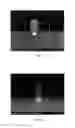
FIG. 1 is a SEM photo of a gate stack profile after the gate stack is etched and before the polymer is removed. The remained polymer (the white thin deposition layer indicated by an arrow A) is obvious at both sides of the gate stack and on the surface of the silicon substrate.
FIG. 2 is a SEM photo of a gate stack profile after the gate stack structure is etched and then the polymer is removed.
DETAILED DESCRIPTION OF THE PREFERRED EMBODIMENTS
The following examples are provided only for explaining the present invention rather than limiting the scope thereof.
step 1), a stack structure of interface SiO2/high-K gate dielectric/metal gate/poly-silicon/hard mask is formed in sequence on a silicon substrate with device isolations formed thereon, wherein the high-K gate dielectric is Hf-base doped oxide, such as HfO2, HfSiON, HfSiO, HfSiON, HfLaO, HfLaON, HfAlON, or HfSiAION, etc., the metal gate comprises metal nitride or doped refractory metal, such as TaN, TiN, TaC, TaCN, MoAlN, TiAlN, TiGaN, or MoAlN, etc., and the hard mask comprises SiO2, Si3N4 or a combination thereof.
step 2), a resist pattern is formed by electron beam lithography.
step 3), the gate stack structure is etched by reactive ion etch, wherein the hard mask is etched by a F-base gas such as CF4/CHF3, the polysilicon is etched by a mixed gas of Cl2/HBr, the metal gate is etched by a Cl-base reactive ion etch using mixed gas such as BCl3/Cl2/Ar or BCl3/Cl2/SF6/Ar, and the high-K gate dielectric is etched by a BCl3-base gas.
step 4), the polymer is removed by wet chemical etching, wherein the etching solution consists of HF, HCl and water, the ratio of HF by volume is 0.2˜1% and the ratio of HCl by volume is 5˜15%. The resultant structure of step 3) is immersed into the etching solution under the room temperature for 10˜60 seconds while the etching solution is stirred to achieve a good uniformity.
A comparison between FIG. 1 and FIG. 2 shows the effect of the removing of the remained polymer according to the present invention. FIG. 2 shows that the polymer at both sides of the gate stack and on the surface of the silicon substrate has been completely removed while the etch profile is still vertical and the silicon surface is smooth without damage.
Claims
1. A method for removing polymer after etching a gate stack structure of high-K gate dielectric/metal gate, comprising:
step 1): forming a gate stack structure of interface SiO2/high-K gate dielectric/metal gate/polysilicon/hard mask in sequence on a silicon substrate with device isolations formed thereon;
step 2): forming a resist pattern by the lithography;
step 3): etching the gate stack structure; and
step 4): immersing the resultant structure of step 3) in an etching solution of HF/HCl/water to remove the polymer, wherein in the etching solution the ratio of HF by volume is 0.2˜1% and the ratio of HCl by volume is 5˜15%.
2. The method according to claim 1, wherein in step 1) the high-K gate dielectric is Hf-base doped oxide.
3. The method according to claim 1, wherein the high-K gate dielectric comprises HfO2, HfSiON, HfSiO, HfSiON, HfLaO, HfLaON, HfAlON, or HfSiAlON.
4. The method according to claim 1, wherein in step 1) the metal gate comprises metal nitride or doped refractory metal.
5. The method according to claim 1, wherein the metal gate comprises TaN, TiN, TaC, TaCN, MoAlN, TiAlN, TiGaN, or MoAlN.
6. The method according to claim 1, wherein in step 1) the hard mask comprises SiO2, Si3N4, or a combination thereof.
7. The method according to claim 1, wherein in step 3), the hard mask is etched by a F-base gas CF4/CHF3, the poly-silicon is etched by a mixed gas of Cl2/HBr, the metal gate is etched by a Cl-base reactive ion etching, and the high-K gate dielectric is etched by a BCl3-base gas.
8. The method according to claim 7, wherein a mixed gas of BCl3/Cl2/Ar or BCl3/Cl2/SF6/Ar is used in the Cl-base reactive ion etching.
9. The method according to claim 1, wherein in step 4), the resultant structure of step 3) is immersed in the etching solution under the room temperature for 10˜120 seconds while the etching solution is stirred.
10. The method according to claim 2, wherein the high-K gate dielectric comprises HfO2, HfSiON, HfSiO, HfLaO, HfLaON, HfAlON, or HfSiAlON.
11. The method according to claim 4, wherein the metal gate comprises TaN, TiN, TaC, TaCN, MoAlN, TiAlN, TiGaN, or MoAlN.
Images & Drawings included:

Sources:
- United States Patent and Trademark Office - verify current appl. status at the USPTO↗
Recent applications in this class:
- » 20230055179 2023-02-23
PREPARATION METHOD OF METAL CONNECTING LINE - » 20210320002 2021-10-14
WATER SOLUBLE POLYMERS FOR PATTERN COLLAPSE MITIGATION - » 20190259600 2019-08-22
Mechanisms for forming patterns using multiple lithography processes - » 20190088470 2019-03-21
Fill material to mitigate pattern collapse - » 20180315594 2018-11-01
Method of cleaning and drying semiconductor substrate - » 20180166272 2018-06-14
Enhanced charged particle beam processes for carbon removal - » 20180138033 2018-05-17
Removal of metal - » 20180033611 2018-02-01
Cluster tool and manufacuturing method of semiconductor structure using the same - » 20170372891 2017-12-28
Mechanisms for forming patterns using multiple lithography processes - » 20170178895 2017-06-22
Method for cleaning substrate
Recent applications for this Assignee:
- » 20250294834 2025-09-18
SEMICONDUCTOR DEVICE AND METHOD OF MANUFACTURING SEMICONDUCTOR DEVICE - » 20250294833 2025-09-18
THIN FILM TRANSISTOR AND METHOD OF MANUFACTURING THIN FILM TRANSISTOR - » 20250266089 2025-08-21
METHOD FOR OPERATING MEMORY CELL AND RESISTIVE RANDOM ACCESS MEMORY, AND ELECTRONIC DEVICE - » 20250240995 2025-07-24
METHOD OF MANUFACTURING VERTICAL DEVICE BY FIRSTLY ETCHING ACTIVE REGION OF DEVICE - » 20250212465 2025-06-26
THIN FILM TRANSISTOR, MEMORY AND METHOD OF MANUFACTURING THIN FILM TRANSISTOR - » 20250112378 2025-04-03
MULTI-BAND AND MULTI-FUNCTIONAL ANTENNA INTEGRATED MODULE AND PREPARATION METHOD THEREOF - » 20250089577 2025-03-13
MEMORY CELL AND METHOD OF MANUFACTURING THE SAME, MEMORY, AND METHOD OF STORING INFORMATION - » 20250063713 2025-02-20
MEMORY WITH THREE-DIMENSIONAL VERTICAL STRUCTURE AND METHOD OF MANUFACTURING MEMORY WITH THREE-DIMENSIONAL VERTICAL STRUCTURE - » 20250054838 2025-02-13
THREE-DIMENSIONAL INTEGRATED CIRCUIT AND MANUFACTURING METHOD THEREFOR - » 20250006556 2025-01-02
SELF-ALIGNED NANOMETER THROUGH-SILICON-VIA STRUCTURE AND METHOD OF PREPARING THE SAME