Method and apparatus for reducing thermopile variations
US20120139077A1
2012-06-07
12/962,257
2010-12-07
✅ Patent granted
US 8,586,395 B2
2013-11-19
-
-
Stephen W Smoot
Alan A. R. Cooper | W. James Brady, III | Frederick J. Telecky, Jr.
2031-07-14
Abstract:
Here, an apparatus is provided. The apparatus generally comprises a substrate and a thermopile. The thermopile includes a cavity that is etched into the substrate, a functional area that is formed over the substrate (where the cavity is generally coextensive with the functional area), and a metal ring formed over the substrate along the periphery of the functional area (where the metal ring is thermally coupled to the substrate).
Inventors:
- Walter Meinel 6 🇺🇸 Tucson, AZ, United States
- Kalin V. Lazarov 12 🇺🇸 Colorado Springs, CO, United States
Assignee:
- TEXAS INSTRUMENTS INCORPORATED 18,931 🇺🇸 Dallas, TX, United States
Applicant:
Interested in similar patents?
Get notified when new applications in this technology area are published.
Classification:
H01L31/101 IPC
Semiconductor devices sensitive to infra-red radiation, light, electromagnetic radiation of shorter wavelength or corpuscular radiation and specially adapted either for the conversion of the energy of such radiation into electrical energy or for the control of electrical energy by such radiation; Processes or apparatus specially adapted for the manufacture or treatment thereof or of parts thereof; Details thereof in which radiation controls flow of current through the device, e.g. photoresistors characterised by at least one potential-jump barrier or surface barrier, e.g. phototransistors Devices sensitive to infra-red, visible or ultra-violet radiation
G01J5/12 » CPC main
Radiation pyrometry, e.g. infrared or optical thermometry using electric radiation detectors using thermoelectric elements, e.g. thermocouples
H01L23/3171 » CPC further
Details of semiconductor or other solid state devices; Encapsulations, e.g. encapsulating layers, coatings, e.g. for protection characterised by the arrangement or shape; Partial encapsulation or coating the coating being directly applied to the semiconductor body, e.g. passivation layer
H01L2924/0002 » CPC further
Indexing scheme for arrangements or methods for connecting or disconnecting semiconductor or solid-state bodies as covered by; Technical content checked by a classifier Not covered by any one of groups , and
H01L2924/00 » CPC further
Indexing scheme for arrangements or methods for connecting or disconnecting semiconductor or solid-state bodies as covered by
H01L23/433 IPC
Details of semiconductor or other solid state devices; Arrangements for cooling, heating, ventilating or temperature compensation ; Temperature sensing arrangements; Fillings or auxiliary members in containers or encapsulations selected or arranged to facilitate heating or cooling Auxiliary members in containers characterised by their shape, e.g. pistons
H01L21/56 IPC
Processes or apparatus adapted for the manufacture or treatment of semiconductor or solid state devices or of parts thereof; Manufacture or treatment of semiconductor devices or of parts thereof the devices having at least one potential-jump barrier or surface barrier, e.g. PN junction, depletion layer or carrier concentration layer; Assembly of semiconductor devices using processes or apparatus not provided for in a single one of the subgroups - , e.g. sealing of a cap to a base of a container Encapsulations, e.g. encapsulation layers, coatings
H01L31/024 IPC
Semiconductor devices sensitive to infra-red radiation, light, electromagnetic radiation of shorter wavelength or corpuscular radiation and specially adapted either for the conversion of the energy of such radiation into electrical energy or for the control of electrical energy by such radiation; Processes or apparatus specially adapted for the manufacture or treatment thereof or of parts thereof; Details thereof; Details Arrangements for cooling, heating, ventilating or temperature compensation
Description
TECHNICAL FIELD
The invention relates generally to thermal stabilization of a thermopile and, more particularly, to the use of a metal ring for thermal stabilization of a thermopile.
BACKGROUND
When a thermopile employs a membrane, it can be important to maintain a generally constant or fixed thermal conductivity for the membrane. However, conventional solutions that have been employed are generally inadequate for many newly developed thermopiles (which employ a membrane). Therefore, there is a need for an apparatus and/or method that maintains a generally constant thermal conductivity for a membrane of a thermopile. An example of a conventional method and/or apparatus is U.S. Patent Pre-Grant Publ. No. 2006/0262829.
SUMMARY
A preferred embodiment of the present invention, accordingly, provides an apparatus. The apparatus comprises a substrate; and a thermopile including: a cavity that is etched into the substrate; a functional area that is formed over the substrate, wherein the cavity is generally coextensive with the functional area; and a metal ring formed over the substrate along the periphery of the functional area, wherein the metal ring is thermally coupled to the substrate.
In accordance with a preferred embodiment of the present invention, the metal ring further comprises a plurality of metallization layers formed over the substrate with thermally conductive layers formed therebetween.
In accordance with a preferred embodiment of the present invention, the metal ring further comprises: a first via layer formed over the substrate; a first metallization layer formed over the first via layer; a second via layer formed over the first metallization layer; a second metallization layer formed over the second via layer; a third via layer formed over the second metallization layer, wherein the first, second, and third via layers are formed of a thermally conductive material; and a third metallization layer that is formed over the third via layer.
In accordance with a preferred embodiment of the present invention, the apparatus further comprises a passivation layer formed over the thermopile.
In accordance with a preferred embodiment of the present invention, the apparatus further comprises a plurality of openings extend through the passivation layer and the functional area to the substrate.
In accordance with a preferred embodiment of the present invention, the apparatus further comprises a cover plate formed over the passivation layer.
In accordance with a preferred embodiment of the present invention, the cover plate is formed of an epoxy, and wherein the first, second, and third via layers are each formed of copper, aluminum, or tungsten, and wherein the first second and third metallization layers are formed of aluminum or copper.
In accordance with a preferred embodiment of the present invention, an apparatus is provided. The apparatus comprises a substrate; a thermopile including: a cavity that is etched into the substrate; a functional area that is formed over the substrate, wherein the cavity is generally coextensive with the functional area; and a metal ring formed over the substrate along the periphery of the functional area, wherein the metal ring is thermally coupled to the substrate; and functional circuitry formed on the substrate and electrically coupled to the thermopile.
In accordance with a preferred embodiment of the present invention, the functional circuitry further comprises an analog-to-digital converter.
In accordance with a preferred embodiment of the present invention, a method is provided. The method comprises forming a plurality of metallization layers and a functional over a substrate, wherein each metallization layer is thermally coupled to the substrate, and wherein the plurality of metallization layers are generally aligned with one another so as to form a metal ring along the periphery of the functional area; forming a passivation layer over the thermopile; forming a plurality of openings that extend through the passivation layer and the functional area to the substrate; and etching the substrate underneath the functional area to form a cavity, wherein the cavity extends to the periphery of the functional area.
In accordance with a preferred embodiment of the present invention, the method further comprises forming a cover plate over the passivation layer to seal the plurality of openings.
In accordance with a preferred embodiment of the present invention, the step of forming the plurality of metallization layers and the thermopile on the substrate further comprises: forming a first via layer formed over the substrate; forming a first metallization layer formed over the first via layer; forming a second via layer formed over the first metallization layer; forming a second metallization layer formed over the second via layer; forming a third via layer formed over the second metallization layer, wherein the first, second, and third via layers are formed of a thermally conductive material; and forming a third metallization layer that is formed over the third via layer.
The foregoing has outlined rather broadly the features and technical advantages of the present invention in order that the detailed description of the invention that follows may be better understood. Additional features and advantages of the invention will be described hereinafter which form the subject of the claims of the invention. It should be appreciated by those skilled in the art that the conception and the specific embodiment disclosed may be readily utilized as a basis for modifying or designing other structures for carrying out the same purposes of the present invention. It should also be realized by those skilled in the art that such equivalent constructions do not depart from the spirit and scope of the invention as set forth in the appended claims.
BRIEF DESCRIPTION OF THE DRAWINGS
For a more complete understanding of the present invention, and the advantages thereof, reference is now made to the following descriptions taken in conjunction with the accompanying drawings, in which:
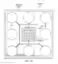
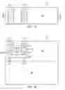
FIG. 1A is a plan view of the layout of an example of an infrared (IR) sensor in accordance with a preferred embodiment of the present invention;
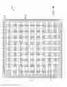
FIG. 1B is a plan view of the layout of the thermopile of FIG. 1;
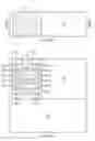
FIG. 2A is plan view of the formation of inner and outer via layers for a portion of the metal ring of FIG. 1B;
FIG. 2B is a cross-sectional view of FIG. 2A along section line 1-1;
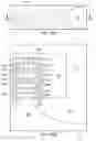
FIG. 3A is plan view of the formation of a metallization layer for a portion of the metal ring of FIG. 1B;
FIG. 3B is a cross-sectional view of FIG. 3A along section line 2-2;
FIG. 4A is plan view of the formation of inner and outer via layers for a portion of the metal ring of FIG. 1B;
FIG. 4B is a cross-sectional view of FIG. 4A along section line 3-3;
FIG. 5A is plan view of the formation of a metallization layer for a portion of the metal ring of FIG. 1B;
FIG. 5B is a cross-sectional view of FIG. 5A along section line 4-4;
FIG. 6A is plan view of the formation of inner and outer via layers for a portion of the metal ring of FIG. 1B;
FIG. 6B is a cross-sectional view of FIG. 6A along section line 5-5;
FIG. 7A is plan view of the formation of a metallization layer for a portion of the metal ring of FIG. 1B;
FIG. 7B is a cross-sectional view of FIG. 7A along section line 6-6;
FIG. 8A is plan view of the formation of inner and outer via layers for a portion of the metal ring of FIG. 1B;
FIG. 8B is a cross-sectional view of FIG. 8A along section line 7-7;
FIG. 9A is plan view of the formation of a metallization layer for a portion of the metal ring of FIG. 1B;
FIG. 9B is a cross-sectional view of FIG. 9A along section line 8-8; and
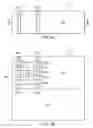
FIG. 10A is a plan view of the formation of the cavity;
FIG. 10B is a cross-sectional view of FIG. 10A along line 9-9;
FIG. 11A is a plan view of the formation of the cover plate; and
FIG. 11B is a cross-sectional view of FIG. 11A along section line 10-10.
DETAILED DESCRIPTION
Refer now to the drawings wherein depicted elements are, for the sake of clarity, not necessarily shown to scale and wherein like or similar elements are designated by the same reference numeral through the several views.
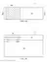
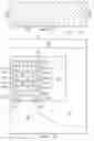
Referring to FIG. 1A of the drawings, the reference numeral 100 generally designates an example of an IR sensor in accordance with a preferred embodiment of the present invention. The IR sensor 100 generally comprises a thermopile 102 and functional circuitry 104 (which may be, for example, an analog-to-digital converter or ADC). The thermopile 102 may be formed on the same die as the functional circuitry 104, and the thermopile 102 is electrically coupled to functional circuitry 104.
Turning to FIG. 1B, thermopile 102 can be seen in greater detail. This thermopile 102 generally comprises functional area 108 that employs the Seebeck effect to generate an electrical current based on a temperature difference between “cold” and “hot” junctions. As part of the formation of the thermopile 102, openings or holes (i.e., 110) are formed in the functional area 108 that penetrate a protective overcoat or passivation layer (i.e., silicon nitride layer) and extends down to the substrate 202 shown in FIG. 2B. This allows the substrate underneath most of the functional area 108 to be etched. The recesses or cavities formed in the substrate from the etching process help to form “hot” junctions in the center of the functional area 108, and “cold” junctions along the periphery of the functional area 108. A metal ring 106 is also formed along the periphery of the functional area 108 of thermopile 102. This metal ring 106 is generally comprised of several metallization layers that are thermally coupled (thermal short) to the substrate. By having this “thermal short,” it allows the functional area 108 (which is membrane) to have a generally fixed or constant thermal conductivity. This generally constant thermal conductivity provides high accuracy and reduces the functional area's 108 sensitivity to fatigue caused by changes in atmospheric pressure.
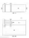
Turning now to FIGS. 2A to 9B, a portion of the process of the formation of the metal ring 106 can be seen for portion 112 of FIG. 1B. Typically, the metal ring 106 is formed at substantially the same time as the functional area 108. The metal ring 106 is generally comprised of an inner barrier ring 222-2 and an outer barrier ring 222-1, where each is formed of a set or stack of thermally conductive layers over substrate 202. These barrier rings 222-1 and 222-2 are generally parallel to one another along the periphery of functional area 108 with a circuit trace region 230 therebetween (which has a circuit trace 212 formed therein). The circuit trace region 230 is generally comprised of a set or stack of dielectric layers 201 (i.e., silicon dioxide); this set of dielectric layers 201 also forms a portion of functional area 108. The stacks of thermally conductive layers forming barrier rings 222-1 and 222-2 generally include inner via layers 204-2, 208-2, 214-2, and 218-2 (which are generally aligned with one another) and outer via layers 204-1, 208-1, 214-1, and 218-1 (which are generally aligned with one another) that are generally continuous strips of thermally conductive materials (i.e., copper, aluminum, tungsten, etc.). Included between the via layers 204-1, 204-2, 208-1, 208-2, 214-1, 214-2, 218-1, and 218-2, are inner metallization layers 210-2 and 216-2 (which are generally aligned with the inner via layers 204-2, 208-2, 214-2, and 218-2) and outer metallization layers 210-1 and 216-1 (which are generally aligned with outer via layers 204-1, 208-1, 214-1, and 218-1). To help isolate a portion of the circuit trace region 230, an upper metallization layer 220 and lower metallization layer 206 are provided, which extend between barrier rings 222-1 and 222-2 through the circuit trace region 230. Additionally, metallization layers 206, 210-1, 210-2, 216-1, 216-2, and 220 are formed of an thermally conductive metal (i.e., aluminum or copper).
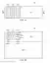
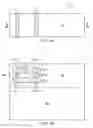
As shown in FIGS. 10A and 10B, a protective overcoat or passivation layer 224 (i.e., silicon nitride layer) is formed over the thermocouple 102, which in many processes is one of the last steps; however, for thermopile 102, openings (i.e., 110) are formed through the protective overcoat 224 and functional area 108 to the substrate 202. The openings (i.e., 110) allow the portion of the substrate 202 underlying the functional area 108 to be etched, which forms cavity 226. In many cases, it can be difficult to control the etching of the cavity 226, so there is a potential for overetching (i.e., etching beyond the periphery of the functional area 108). The metal ring 106, nonetheless, can stabilize the thermal conductivity of the functional area 108. Finally, after the cavity 226 has been etched, a cover plate 228 (which can be formed of an epoxy) can be formed over the protective overcoat 224 so as to seal the openings (i.e., 110).
Having thus described the present invention by reference to certain of its preferred embodiments, it is noted that the embodiments disclosed are illustrative rather than limiting in nature and that a wide range of variations, modifications, changes, and substitutions are contemplated in the foregoing disclosure and, in some instances, some features of the present invention may be employed without a corresponding use of the other features. Accordingly, it is appropriate that the appended claims be construed broadly and in a manner consistent with the scope of the invention.
Claims
1. An apparatus comprising:
a substrate; and
a thermopile including:
a cavity that is etched into the substrate;
a functional area that is formed over the substrate, wherein the cavity is generally coextensive with the functional area; and
a metal ring formed over the substrate along the periphery of the functional area, wherein the metal ring is thermally coupled to the substrate.
2. The apparatus of claim 1, wherein the metal ring further comprises a plurality of metallization layers formed over the substrate with thermally conductive layers formed therebetween.
3. The apparatus of claim 2, wherein the metal ring further comprises:
a first via layer formed over the substrate;
a first metallization layer formed over the first via layer;
a second via layer formed over the first metallization layer;
a second metallization layer formed over the second via layer;
a third via layer formed over the second metallization layer, wherein the first, second, and third via layers are formed of a thermally conductive material; and
a third metallization layer that is formed over the third via layer.
4. The apparatus of claim 3, wherein the apparatus further comprises a passivation layer formed over the thermopile.
5. The apparatus of claim 4, wherein the apparatus further comprises a plurality of openings extend through the passivation layer and the functional area to the substrate.
6. The apparatus of claim 5, wherein the apparatus further comprises a cover plate formed over the passivation layer.
7. The apparatus of claim 6, wherein the cover plate is formed of an epoxy, and wherein the first, second, and third via layers are each formed of copper, aluminum, or tungsten, and wherein the first second and third metallization layers are formed of aluminum or copper.
8. An apparatus comprising:
a substrate;
a thermopile including:
a cavity that is etched into the substrate;
a functional area that is formed over the substrate, wherein the cavity is generally coextensive with the functional area; and
a metal ring formed over the substrate along the periphery of the functional area, wherein the metal ring is thermally coupled to the substrate; and
functional circuitry formed on the substrate and electrically coupled to the thermopile.
9. The apparatus of claim 8, wherein the metal ring further comprises a plurality of metallization layers formed over the substrate with thermally conductive layers formed therebetween.
10. The apparatus of claim 9, wherein the metal ring further comprises:
a first via layer formed over the substrate;
a first metallization layer formed over the first via layer;
a second via layer formed over the first metallization layer;
a second metallization layer formed over the second via layer;
a third via layer formed over the second metallization layer, wherein the first, second, and third via layers are formed of a thermally conductive material; and
a third metallization layer that is formed over the third via layer.
11. The apparatus of claim 10, wherein the apparatus further comprises a passivation layer formed over the thermopile.
12. The apparatus of claim 11, wherein the apparatus further comprises a plurality of openings extend through the passivation layer and functional area to the substrate.
13. The apparatus of claim 12, wherein the apparatus further comprises a cover plate formed over the passivation layer.
14. The apparatus of claim 13, wherein the cover plate is formed of an epoxy, and wherein the first, second, and third via layers are each formed of copper, aluminum, or tungsten, and wherein the first second and third metallization layers are formed of aluminum or copper.
15. The apparatus of claim 14, wherein the functional circuitry further comprises an analog-to-digital converter.
16. A method comprising:
forming a plurality of metallization layers and a functional over a substrate, wherein each metallization layer is thermally coupled to the substrate, and wherein the plurality of metallization layers are generally aligned with one another so as to form a metal ring along the periphery of the functional area;
forming a passivation layer over the thermopile;
forming a plurality of openings that extend through the passivation layer and the functional area to the substrate; and
etching the substrate underneath the functional area to form a cavity, wherein the cavity extends to the periphery of the functional area.
17. The method of claim 16, wherein the method further comprises forming a cover plate over the passivation layer to seal the plurality of openings.
18. The method of claim 17, wherein the step of forming the plurality of metallization layers and the thermopile on the substrate further comprises:
forming a first via layer formed over the substrate;
forming a first metallization layer formed over the first via layer;
forming a second via layer formed over the first metallization layer;
forming a second metallization layer formed over the second via layer;
forming a third via layer formed over the second metallization layer, wherein the first, second, and third via layers are formed of a thermally conductive material; and
forming a third metallization layer that is formed over the third via layer.
19. The apparatus of claim 18, wherein the cover plate is formed of an epoxy, and wherein the first, second, and third via layers are each formed of copper, aluminum, or tungsten, and wherein the first second and third metallization layers are formed of aluminum or copper.
Images & Drawings included:
Sources:
- United States Patent and Trademark Office - verify current appl. status at the USPTO↗
Recent applications in this class:
- » 20250283762 2025-09-11
PHOTODETECTOR PIXEL, PHOTODETECTOR AND METHODS OF FORMING THE SAME - » 20250180407 2025-06-05
TEMPERATURE SENSING DEVICE - » 20250146877 2025-05-08
INFRARED SHACK-HARTMANN WAVEFRONT SENSOR BASED ON CAVITY-COUPLED NANOANTENNAS - » 20250137848 2025-05-01
THERMAL SENSOR ARRAY DEVICE, METHOD OF MEASURING A TEMPERATURE GRADIENT AND METHOD OF MEASURING A TEMPERATURE - » 20250027818 2025-01-23
SENSOR, IMAGING DEVICE AND ELECTRONIC DEVICE - » 20250003803 2025-01-02
OPTICAL SENSOR - » 20240210248 2024-06-27
SENSOR ELEMENT, AND SENSOR DEVICE - » 20240125652 2024-04-18
MODULAR INFRARED SENSOR MODULE FOR COOKING - » 20240125651 2024-04-18
OPTICAL SENSOR - » 20240068875 2024-02-29
THERMOPILE SENSOR AND SENSOR ARRAY
Recent applications for this Assignee:
- » 20250291595 2025-09-18
CIRCUIT, SYSTEM, AND METHOD FOR MATRIX DECIMATION - » 20250286550 2025-09-11
TRANSISTOR SHUTDOWN CIRCUT - » 20250279725 2025-09-04
CONDUCTION MODE CONTROL - » 20250274138 2025-08-28
SWITCH REGULATOR - » 20250267687 2025-08-21
ENHANCED BROADCAST TRANSMISSION IN UNSLOTTED CHANNEL HOPPING MEDIUM ACCESS CONTROL - » 20250266825 2025-08-21
BOOTSTRAP CIRCUIT - » 20250247097 2025-07-31
LEVEL SHIFTER CIRCUIT - » 20250247082 2025-07-31
LOW AREA AND POWER MULTI-BIT FLIP-FLOP - » 20250246995 2025-07-31
SWITCHING CONVERTER DEADTIME CONTROL - » 20250246345 2025-07-31
TRIMMING RESISTOR USING MODULATED SIGNAL