Driving module for digital visual interface
US20120162174A1
2012-06-28
13/086,214
2011-04-13
✅ Patent granted
US 8,952,743 B2
2015-02-10
-
-
Brandon S Cole
Novak Druce Connolly Bove + Quigg LLP
2033-09-12
Abstract:
A driving module for driving a Digital Visual Interface includes an integrated chip, a pull-up resistor unit, and a voltage converter. The pull-up resistor unit includes a plurality of resistors. The voltage converter includes an array of resistors comprising a plurality of resistors and a MOSFET. Each resistor of the array of resistors includes a first end and a second end. The first ends are electrically connected to outputs of the integrated chip, and the second ends are electrically connected to a drain of the MOSFET. A source of the MOSFET is connected to ground, and a gate of the MOSFET is electrically connected to an output of the main board.
Assignee:
- HON HAI PRECISION INDUSTRY CO., LTD. 12,833 🇹🇼 Tu-Cheng, Taiwan
- HONG FU JIN PRECISION INDUSTRY (SHENZHEN) CO., LTD. 4,225 🇨🇳 Shenzhen City, China
- Scienbizip Consulting (Shenzhen) Co., Ltd. 24 🇨🇳 Guangdong, China
Applicant:
Interested in similar patents?
Get notified when new applications in this technology area are published.
Classification:
G09G2370/12 » CPC further
Aspects of data communication Use of DVI or HDMI protocol in interfaces along the display data pipeline
G06F3/038 IPC
Input arrangements for transferring data to be processed into a form capable of being handled by the computer; Output arrangements for transferring data from processing unit to output unit, e.g. interface arrangements; Input arrangements or combined input and output arrangements for interaction between user and computer; Arrangements for converting the position or the displacement of a member into a coded form; Pointing devices displaced or positioned by the user, e.g. mice, trackballs, pens or joysticks ; Accessories therefor Control and interface arrangements therefor, e.g. drivers or device-embedded control circuitry
G09G5/006 » CPC main
Control arrangements or circuits for visual indicators common to cathode-ray tube indicators and other visual indicators; Details of a display terminal, the details relating to the control arrangement of the display terminal and to the interfaces thereto Details of the interface to the display terminal
G09G2330/026 » CPC further
Aspects of power supply; Aspects of display protection and defect management; Details of power systems and of start or stop of display operation Arrangements or methods related to booting a display
H03K17/687 IPC
Electronic switching or gating, i.e. not by contact-making and –breaking characterised by the components used by the use, as active elements, of semiconductor devices the devices being field-effect transistors
G09G5/00 IPC
Control arrangements or circuits for visual indicators common to cathode-ray tube indicators and other visual indicators
Description
BACKGROUND
1. Technical Field
The present disclosure relates to driving modules and, more particularly to a driving module for a Digital Visual Interface (DVI).
2. Description of Related Art
An electronic device, such as a notebook, generally includes a hardware driver electrically connected to an output of the mainframe for driving the DVI. However, the working voltage of the DVI is 3 volts, but the pull-up resistor of the DVI usually pulls the voltage output from the chip of the hardware driver from zero to 3.3 volts; so it needs an added voltage converter circuit for adjusting the voltage to the DVI.
Therefore, what is needed is a driving module to overcome the above described shortcomings
BRIEF DESCRIPTION OF THE DRAWING
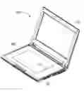
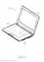
FIG. 1 is an assembled, isometric view of a notebook, in accordance with an exemplary embodiment of the present disclosure.
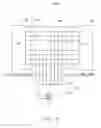
FIG. 2 is a circuit diagram of a driving module of FIG. 1.
DETAILED DESCRIPTION
Referring to FIGS. 1 to 2, an exemplary embodiment of a driving module 100 is shown. In the present embodiment, the driving module 100 is used for driving a DVI 20 of a notebook 200. The notebook 200 also includes a main board 300.
The driving module 100 includes an integrated chip 30, a pull-up resistor unit 40 electrically connected to an output of the chip 30, and a voltage converter unit 50.
In the present embodiment, the integrated chip 30 is driven by the main board 300 of the notebook 200. The chip 30 includes two groups of outputs for outputting driving signals. Each group includes three digital pins and a clock pin. A plurality of filter capacitors 60 (eight in this embodiment) each have a first end electrically connected to one corresponding output of the integrated chip 30. The filter capacitors 60 are configured for filtering direct signals output from the integrated chip 30; therefore, the integrated chip 30 only outputs alternating signals.
The pull-up resistor unit 40 includes eight resistors. Each resistor of the pull-up resistor unit 40 is electrically connected between a second end of one corresponding filter capacitor 60 and an input of the DVI 20.
The voltage converter unit 50 includes an array of resistors 51 and a MOSFET 52. In the present embodiment, the MOSFET 52 is an N-type depletion mode MOSFET. The array of resistors 51 includes eight resistors. One end of each of the eight resistors of the array of resistors 51 is electrically connected to the second end of one corresponding filter capacitors 60. The other ends of the eight resistors of the array of resistors 51 are all electrically connected to the drain of the MOSFET 52. The source of the MOSFET 52 is connected to ground. The gate of the MOSFET 52 is electrically connected to a voltage V1 output from the main board 300, which is about 3.3 volts.
At the initial of start up of the notebook 200, by supplying external power thereto, there is no voltage output from the main board 300 instantly. Therefore, the MOSFET 52 turns off because of the voltage V1 is zero, and it can prevent the array of resistors 51 from connecting to ground directly and damaging or destroying the DVI 20 at that moment. After driving the main board 300, the MOSFET 52 is in on-state. The pull-up resistor unit 40 pulls the voltage output from the integrated chip 30 to 3.3 volts, and the array of resistors 51 of the voltage converter unit 50 adjusts the voltage to 3 volts as the working voltage of the DVI 20.
It is to be further understood that even though numerous characteristics and advantages have been set forth in the foregoing description of embodiments, together with details of the structures and functions of the embodiments, the disclosure is illustrative only; and that changes may be made in detail, especially in matters of shape, size, and arrangement of parts within the principles of the disclosure to the full extent indicated by the broad general meaning of the terms in which the appended claims are expressed.
Claims
What is claimed is:1. A driving module for driving a Digital Visual Interface (DVI) of a computer comprising a main board, the driving module comprising:
an integrated chip with a plurality of outputs;
a pull-up resistor unit comprising a plurality of resistors, one end of each resistor of the pull-up resistor unit being electrically connected to one of the plurality of outputs of the integrated chip, and the other end of each resistor of the pull-up resistor unit being electrically connected to one input of the DVI;
a voltage converter comprising an array of resistors comprising a plurality of resistors and a MOSFET, each resistor of the array of resistors comprising a first end and a second end, the first ends being electrically connected to outputs of the integrated chip, and the second ends being electrically connected to a drain of the MOSFET, a source of the MOSFET being connected to ground, and a gate of the MOSFET being electrically connected to an output of the main board.
2. The driving module of claim 1, wherein the integrated chip comprises eight outputs.
3. The driving module of claim 2, wherein the array of resistors comprises eight resistors, each first end being electrically connected to one output of the integrated chip.
4. The driving module of claim 1, further comprising a plurality of filter capacitors electrically connected between the outputs of the integrated chip and the resistors of the pull-up resistor unit, respectively.
5. The driving module of claim 1, wherein a plurality of filter capacitors are electrically connected between the outputs of the integrated chip and the resistors of array of resistors, respectively.
6. The driving module of claim 1, further comprising a plurality of filter capacitors electrically connected between the outputs of the integrated chip and the resistors of array of resistors, respectively.
7. The driving module of claim 1, wherein the MOSFET is an N-type depletion mode MOSFET.
8. The driving module of claim 1, wherein the output of the main board is 3.3 volt.
Images & Drawings included:
Sources:
- United States Patent and Trademark Office - verify current appl. status at the USPTO↗
Recent applications in this class:
- » 20250259605 2025-08-14
ELECTRONIC DEVICE FOR PROVIDING POWER TO DISPLAY - » 20250246166 2025-07-31
ELECTRONIC DEVICE AND PROCESSING METHOD - » 20250246165 2025-07-31
DISPLAY APPARATUS - » 20250225950 2025-07-10
REMOTE CONTROL OF FUNCTIONAL PARAMETERS AND RENDERING OF OPERATIONAL PREVIEW OF ELECTRONIC DEVICE - » 20250191552 2025-06-12
DISPLAY DEVICES - » 20250174210 2025-05-29
DISPLAY DEVICE INPUT CIRCUIT, DISPLAY DEVICE AND CONTROL METHOD THEREOF - » 20250149008 2025-05-08
METHOD FOR SHORTENING DISPLAY LATENCY BASED ON VARIABLE REFRESH RATE TECHNOLOGY AND RELATED RENDERING DEVICE THEREOF - » 20250118275 2025-04-10
CLIENT-SERVER VISUALIZATION SYSTEM WITH HYBRID DATA PROCESSING - » 20250118274 2025-04-10
DISPLAY SYSTEM AND OPERATION METHOD FOR DISPLAY SYSTEM - » 20250104666 2025-03-27
DISPLAY DEVICE
Recent applications for this Assignee:
- » 20150043296 2015-02-12
Serial advanced technology attachment dual in-line memory module device - » 20140317587 2014-10-23
Computing device and method for testing layout of power pin of chipset on circuit board - » 20140233961 2014-08-21
Optical communication module including optical-electrical signal converters and optical signal generators - » 20140173885 2014-06-26
Method for manufacturing light emitting diode module - » 20140154900 2014-06-05
Circuit board assembly having two members rotating in opposite directions - » 20140083669 2014-03-27
HEAT SINK - » 20140083669 2014-03-27
HEAT SINK - » 20140063746 2014-03-06
Electronic device with heat dissipation assembly - » 20140061224 2014-03-06
AUTOMATIC VENDING MACHINE - » 20140060914 2014-03-06
Enclosure with shield apparatus