Light-emitting device
US20120170276A1
2012-07-05
13/342,632
2012-01-03
✅ Patent granted
US 8,708,532 B2
2014-04-29
-
-
Britt D Hanley
Rajesh Vallabh | Foley Hoag LLP
2032-12-22
Abstract:
A light-emitting device includes: a transparent substrate including a mounting surface, a circuit path formed on the mounting surface, and two opposite contacts formed on the mounting surface; a light-emitting diode chip that includes two electrodes and that is mounted on the mounting surface; and a reflecting cup disposed on the mounting surface to cover the light-emitting diode chip. The reflecting cup is formed with an inner recess that faces the mounting surface, and a reflecting layer formed on a recess-defining wall that defines the inner recess. The reflecting layer is capable of reflecting light from the light-emitting diode chip toward the transparent substrate.
Applicant:
Interested in similar patents?
Get notified when new applications in this technology area are published.
Classification:
H01L33/486 » CPC main
Semiconductor devices with at least one potential-jump barrier or surface barrier specially adapted for light emission; Processes or apparatus specially adapted for the manufacture or treatment thereof or of parts thereof; Details thereof characterised by the semiconductor body packages; Containers adapted for surface mounting
F21V7/06 IPC
Reflectors for light sources; Optical design with parabolic curvature
F21K9/68 » CPC further
Light sources using semiconductor devices as light-generating elements, e.g. using light-emitting diodes [LED] or lasers; Optical arrangements integrated in the light source, e.g. for improving the colour rendering index or the light extraction Details of reflectors forming part of the light source
H01L25/0753 » CPC further
Assemblies consisting of a plurality of individual semiconductor or other solid state devices ; Multistep manufacturing processes thereof all the devices being of a type provided for in the same subgroup of groups - , e.g. assemblies of rectifier diodes the devices not having separate containers the devices being of a type provided for in group the devices being arranged next to each other
H01L2924/00014 » CPC further
Indexing scheme for arrangements or methods for connecting or disconnecting semiconductor or solid-state bodies as covered by; Technical content checked by a classifier the subject-matter covered by the group, the symbol of which is combined with the symbol of this group, being disclosed without further technical details
H01L2924/00 » CPC further
Indexing scheme for arrangements or methods for connecting or disconnecting semiconductor or solid-state bodies as covered by
F21K9/00 » CPC further
Light sources using semiconductor devices as light-generating elements, e.g. using light-emitting diodes [LED] or lasers
F21V29/00 IPC
Protecting lighting devices from thermal damage; Cooling or heating arrangements specially adapted for lighting devices or systems
H01L33/48 IPC
Semiconductor devices with at least one potential-jump barrier or surface barrier specially adapted for light emission; Processes or apparatus specially adapted for the manufacture or treatment thereof or of parts thereof; Details thereof characterised by the semiconductor body packages
H01L33/60 » CPC further
Semiconductor devices with at least one potential-jump barrier or surface barrier specially adapted for light emission; Processes or apparatus specially adapted for the manufacture or treatment thereof or of parts thereof; Details thereof characterised by the semiconductor body packages; Optical field-shaping elements Reflective elements
Description
CROSS-REFERENCE TO RELATED APPLICATION
This application claims priority Taiwanese application no. 100 00443, filed on Jan. 5 2011.
BACKGROUND OF THE INVENTION
1. Field of the Invention
The present invention relates to a light-emitting device, more particularly to a light-emitting device having enhanced brightness.
2. Description of the Related Art
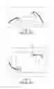
Referring to FIGS. 1 and 2, a conventional light-emitting device generally comprises a light-emitting diode chip 1, electrodes 11, and conductive wires 12 for electrically connecting the electrodes 11 to other electrical components. The light-emitting chip 1 has a main light-emitting surface 10 on which one of the electrodes 11 is disposed. Therefore, at least about 30% of light emitted from the main light-emitting surface 10 may be obstructed by the electrode 11 and the conductive wire 12 and can not be completely utilized. On the other hand, the light emitted from other five surfaces of the light-emitting diode chip 1, i.e., the surfaces other than the main light-emitting surface 10, can not be efficiently utilized. Therefore, it is desirable to provide a light-emitting device that has effective light utilization.
SUMMARY OF THE INVENTION
Therefore, the object of the present invention is to provide a light-emitting device that can overcome the aforesaid drawbacks associated with the prior art.
Accordingly, a light-emitting device of the present invention comprises: a transparent substrate including a mounting surface, a circuit path formed on the mounting surface, and two opposite contacts formed on the mounting surface to respectively connect to two opposite ends of the circuit path; a light-emitting diode chip that includes two electrodes and that is mounted on the mounting surface such that the electrodes are electrically connected to the circuit path; and a reflecting cup disposed on the mounting surface to cover the light-emitting diode chip in a manner that the contacts are exposed from the reflecting cup, the reflecting cup being formed with an inner recess that faces the mounting surface, and a reflecting layer formed on a recess-defining wall that defines the inner recess, the reflecting layer being capable of reflecting light from the light-emitting diode chip toward the transparent substrate.
BRIEF DESCRIPTION OF THE DRAWINGS
Other features and advantages of the present invention will become apparent in the following detailed description of the preferred embodiments with reference to the accompanying drawings, of which:
FIG. 1 is schematic side view of a conventional light-emitting device;
FIG. 2 is a schematic top view of the conventional light-emitting device of FIG. 1;
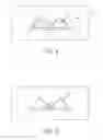
FIG. 3 is a fragmentary exploded perspective view of the first preferred embodiment of a light-emitting device according to the present invention;
FIG. 4 is a schematic side view of the light-emitting device of the first preferred embodiment; and
FIG. 5 is a schematic side view of a modification of the first preferred embodiment.
DETAILED DESCRIPTION OF THE PREFERRED EMBODIMENTS
Before the present invention is described in greater detail, it should be noted that like-components are assigned the same reference numerals throughout the following disclosure.
FIG. 3 is an exploded perspective view of the first preferred embodiment of a light-emitting device according to the present invention.
As shown in FIGS. 3 and 4, in the first preferred embodiment, the light-emitting device of this invention comprises a transparent substrate 2, a plurality of light-emitting diode chips 3, and a reflecting cup 4.
In this embodiment, the transparent substrate 2 is made of glass. Alternatively, the transparent substrate 2 may be made of any other suitable materials as long as it is sufficiently light-transmissible. Preferably, the transparent substrate 2 is made of a material that has light-transmission and heat dissipation properties. The transparent substrate includes a mounting surface 20, a circuit path 21 formed on the mounting surface 20, and two opposite contacts 22 formed on the mounting surface 20 to respectively electrically connect to two opposite ends of the circuit path 21. In this embodiment, the circuit path 21 is made from indium tin oxide (ITO).
Each of the light-emitting diode chips 3 includes two electrodes 31 and may be mounted on the mounting surface 20 of the transparent substrate 2. in any suitable manner such that the electrodes 31 are electrically connected to the circuit path 21. In this embodiment, the light-emitting diode chips 3 are flip-chip mounted on the mounting surface 20. Of course, the light-emitting diode chips 3 may be mounted on the mounting surface 20 by wire bonding.
The reflecting cup 4 is disposed on the mounting surface 20 to cover the light-emitting diode chips 3 in a manner that the contacts 22 are completely or partly exposed from the reflecting cup 4, thereby allowing the contacts 22 to electrically connect to an external circuit (not shown). The reflecting cup 4 may be made of any suitable material that has a good heat-dissipation effect. In addition, the reflecting cup 4 is formed with an inner recess 40 that faces the mounting surface 20, and a reflecting layer 41 formed on a recess-defining wall that defines the inner recess 40. The reflecting layer 41 is capable of reflecting light from surfaces of the light-emitting diode chips 3 toward the transparent substrate 2.
In this embodiment, the inner recess 40 has a cross-section in a substantially inverted. W-shape. It is noted that the inner recess 40 may have a cross-section in a substantially inverted V-shape. Alternatively, the inner recess 40 may have a cross-section in any other shape as long as the reflecting layer 41 is capable of reflecting light from the light-emitting diode chips 3 toward the transparent substrate 2.
In this embodiment, a heat-dissipation filler 5 that is made of a heat-dissipating material is filled in a space cooperatively defined by the reflecting layer 41 on the recess-defining wall and the mounting surface 20. The heat-dissipation filler 5 may be in a liquid, solid, vapor, or gel-like form.
FIG. 5 shows a modification of the first preferred embodiment. Specifically, as shown in FIG. 5, a portion of the reflecting layer 41 on the recess-defining wall of the reflecting cup 4 contacts the light-emitting diode chips 3, thereby facilitating heat dissipation. In this modification, since a part of the reflecting layer 41 is in contact with the light--emitting diode chips 3, there is no need for filling a heat-dissipation filler 5 in the space cooperatively defined by the reflecting layer 41 and the mounting surface 20. Of course, the heat-dissipation filler 5 may also be added in the space.
By virtue of the abovementioned structure, since the light from the light-emitting diode chips 3 may be reflected toward the transparent substrate 2 through the reflecting cup 4, the light from the surfaces of the light-emitting diode chips 3 may be utilized effectively. Therefore, the light-emitting device of the present invention could have enhanced brightness.
While the present invention has been described in connection with what are considered the most practical and preferred embodiments, it is understood that this invention is not limited to the disclosed embodiments but is intended to cover various arrangements included within the spirit and scope of the broadest interpretation so as to encompass all such modifications and equivalent arrangements.
Claims
What is claimed is:1. A light-emitting device comprising:
a transparent substrate including a mounting surface, a circuit path formed on said mounting surface, and two opposite contacts formed on said mounting surface to respectively connect to two opposite ends of said circuit Path;
a light-emitting diode chip that includes two electrodes and that is mounted on said mounting surface such that said electrodes are electrically connected to said circuit path; and
a reflecting cup disposed on said mounting surface to cover said light-emitting diode chip in a manner that said contacts are exposed from said reflecting cup, said reflecting cup being formed with an inner recess that faces said mounting surface, and a reflecting layer formed on a recess-defining wall that defines said inner recess, said reflecting layer being capable of reflecting light from said light-emitting diode chip toward said transparent substrate.
2. The light-emitting device claim 1, further comprising a heat-dissipation filler that is filled in a space cooperatively defined by said reflecting layer on said recess-defining wall and said mounting surface.
3. The light-emitting device of claim 2, wherein said heat-dissipation filler is in one of liquid, solid, vapor, or gel-like form.
4. The light-emitting device of Claim 1, wherein a portion of said reflecting layer on said recess-defining wall contacts said light-emitting diode chip.
5. The light-emitting device of claim 1, wherein said inner recess has a cross-section in a substantially inverted W-shape.
6. The light-emitting device of claim 1, wherein said inner recess has a cross-section in a substantially inverted V-shape.
7. The light-emitting device of claim 1, wherein said light-emitting diode chip is flip-chip mounted on said mounting surface.
Images & Drawings included:


Sources:
- United States Patent and Trademark Office - verify current appl. status at the USPTO↗
Similar patent applications:
- » 20230143281
COMPOSITION FOR LIGHT-EMITTING DEVICE, LIGHT-EMITTING DEVICE, LIGHT-EMITTING APPARATUS, ELECTRONIC DEVICE, AND LIGHTING DEVICE - » 20120153328
Light-emitting device, light-emitting device package, method of manufacturing light-emitting device, and method of packaging light-emitting device - » 20130299788
Organic light-emitting device, coating liquid for forming organic light-emitting device, material for forming organic light-emitting device, light source device using organic light-emitting device, and organic light-emitting device producing method - » 20140159072
Light-emitting device, light-emitting device assembly, and electrode-bearing substrate in which a fragile region is formed in a substrate, and light emitting device cut from light-emitting device assembly - » 20210371427
Organic Compound, Light-Emitting Device Material, Light-Emitting Device, Light-Emitting Apparatus, Light-Emitting Module, Electronic Device, and Lighting Device - » 20240276856
PREPARATION METHOD OF LIGHT-EMITTING DEVICE, LIGHT-EMITTING DEVICE AND LIGHT-EMITTING APPARATUS - » 20090159902
Flip-chip type semiconductor light-emitting device, method for manufacturing flip-chip type semiconductor light-emitting device, printed circuit board for flip-chip type semiconductor light-emitting device, mounting structure for flip-chip type semiconductor light-emitting device, and light-emitting diode lamp - » 20230265305
INK COMPOSITION FOR LIGHT-EMITTING DEVICE, LIGHT-EMITTING DEVICE MANUFACTURED USING INK COMPOSITION, AND ELECTRONIC APPARATUS INCLUDING LIGHT-EMITTING DEVICE - » 20220216444
Composition for manufacturing light-emitting device, light-emitting device manufactured by the same, and method of manufacturing the light-emitting device - » 20240414932
COMPOSITION FOR MANUFACTURING LIGHT-EMITTING DEVICE, LIGHT-EMITTING DEVICE MANUFACTURED BY THE SAME, AND METHOD OF MANUFACTURING THE LIGHT-EMITTING DEVICE
Recent applications in this class:
- » 20250063861 2025-02-20
LIGHT EMITTING MODULE HAVING LIGHT EMITTING DEVICE AND DISPLAY APPARATUS HAVING SAME - » 20250048800 2025-02-06
BASE MEMBER FOR LIGHT EMITTING DEVICE - » 20250040313 2025-01-30
LIGHT EMITTING DEVICE AND LIGHT EMITTING MODULE INCLUDING THE SAME - » 20250040311 2025-01-30
LED CIRCUIT BOARD AND LIGHT EMITTING MODULE - » 20250015235 2025-01-09
METHOD FOR ATTACHING MICRO LEDS TO DISPLAY BY USING FLUID AS SOFT LANDING MEDIUM FOR MICRO LEDS - » 20250006869 2025-01-02
LIGHT EMITTING DIODE PACKAGE AND METHOD OF MANUFACTURING THE SAME - » 20240429350 2024-12-26
OPTOELECTRONIC COMPONENT - » 20240413270 2024-12-12
SEMICONDUCTOR LIGHT-EMITTING APPARATUS - » 20240363809 2024-10-31
Display Device - » 20240363808 2024-10-31
OPTOELECTRONIC SEMICONDUCTOR COMPONENT AND PRODUCTION METHOD