Ge-on-insulator structure and method for forming the same
US20120187487A1
2012-07-26
13/201,903
2011-07-07
✅ Patent granted
US 8,772,873 B2
2014-07-08
WO; PCT/CN2011/077703; 20110727
WO; WO2012/100519; 20120802
William F Kraig | Pavel Ivanov
Hodgson Russ LLP
2032-06-28
Abstract:
A method for forming a Ge-on-insulator structure is provided, comprising steps of: forming a Ge layer (1200) on a substrate (2000); treating a first surface of the Ge layer (1200) to form a first semiconducting metal-germanide passivation layer (1300); bonding the first semiconducting metal-germanide passivation layer (1300) with a silicon substrate (1100), wherein on a surface of the silicon substrate (1100) an oxide insulating layer is formed; and removing the substrate (2000). Further, a Ge-on-insulator structure formed by the method is also provided.
Inventors:
Assignee:
- Tsinghua University 3,118 🇨🇳 Beijing, China
Applicant:
Interested in similar patents?
Get notified when new applications in this technology area are published.
Classification:
H01L21/762 IPC
Processes or apparatus adapted for the manufacture or treatment of semiconductor or solid state devices or of parts thereof; Manufacture or treatment of devices consisting of a plurality of solid state components formed in or on a common substrate or of parts thereof; Manufacture of integrated circuit devices or of parts thereof; Manufacture of specific parts of devices defined in group; Making of isolation regions between components Dielectric regions, e.g. EPIC dielectric isolation, LOCOS; Trench refilling techniques, SOI technology, use of channel stoppers
H01L21/28255 » CPC further
Processes or apparatus adapted for the manufacture or treatment of semiconductor or solid state devices or of parts thereof; Manufacture or treatment of semiconductor devices or of parts thereof the devices having at least one potential-jump barrier or surface barrier, e.g. PN junction, depletion layer or carrier concentration layer the devices having semiconductor bodies comprising elements of Group IV of the Periodic System or AB compounds with or without impurities, e.g. doping materials; Manufacture of electrodes on semiconductor bodies using processes or apparatus not provided for in groups -; Making conductor-insulator-semiconductor electrodes the insulator being formed after the semiconductor body, the semiconductor belonging to Group IV and not being elemental silicon, e.g. Ge, SiGe, SiGeC
H01L27/12 IPC
Devices consisting of a plurality of semiconductor or other solid-state components formed in or on a common substrate including semiconductor components specially adapted for rectifying, oscillating, amplifying or switching and having at least one potential-jump barrier or surface barrier; including integrated passive circuit elements with at least one potential-jump barrier or surface barrier the substrate being other than a semiconductor body, e.g. an insulating body
H01L29/786 IPC
Semiconductor devices adapted for rectifying, amplifying, oscillating or switching, or capacitors or resistors with at least one potential-jump barrier or surface barrier, e.g. PN junction depletion layer or carrier concentration layer; Details of semiconductor bodies or of electrodes thereof; Multistep manufacturing processes therefor; Types of semiconductor device ; Multistep manufacturing processes therefor controllable by only the electric current supplied, or only the electric potential applied, to an electrode which does not carry the current to be rectified, amplified or switched; Unipolar devices, e.g. field effect transistors; Field effect transistors with field effect produced by an insulated gate Thin film transistors, i.e. transistors with a channel being at least partly a thin film
H01L21/28 IPC
Processes or apparatus adapted for the manufacture or treatment of semiconductor or solid state devices or of parts thereof; Manufacture or treatment of semiconductor devices or of parts thereof the devices having at least one potential-jump barrier or surface barrier, e.g. PN junction, depletion layer or carrier concentration layer the devices having semiconductor bodies comprising elements of Group IV of the Periodic System or AB compounds with or without impurities, e.g. doping materials Manufacture of electrodes on semiconductor bodies using processes or apparatus not provided for in groups -
H01L29/66 IPC
Semiconductor devices adapted for rectifying, amplifying, oscillating or switching, or capacitors or resistors with at least one potential-jump barrier or surface barrier, e.g. PN junction depletion layer or carrier concentration layer; Details of semiconductor bodies or of electrodes thereof; Multistep manufacturing processes therefor Types of semiconductor device ; Multistep manufacturing processes therefor
Description
FIELD
The present disclosure relates to a semiconductor manufacture and design, and more particularly to a GeOI (Ge-on-insulator) structure and a method for forming the same.
BACKGROUND
For a long time, a feature size of a metal-oxide-semiconductor field-effect transistor (MOSFET) is scaled down according to Moore's law, and a working speed of the MOSFET is faster and faster. However, physical and technical limits of Si materials have been reached. Therefore, in order to improve a performance of the MOSFET, various methods have been proposed, and consequently a More-than-Moore era has come. Among them, an effective technology is a high-mobility channel engineering based on heterogeneous materials, particularly, high-carrier-mobility materials such as Si-based Ge materials. For example, one high-hole-mobility Si-based Ge material is a GeOI structure formed by directly bonding Ge and a Si wafer having a SiO2 insulating layer, which has good application perspective.
A conventional GeOI structure is formed by directly bonding Ge and insulation oxides such as SiO2, or formed by forming GeO2 on Ge and then bonding Ge and a silicon wafer. The defects lie in that, if a Ge layer is directly formed on an insulation oxide substrate, because an interface between the Ge materials and the insulation oxides is poor, particularly, an interface state density is very high, serious scattering and leakage may be caused, thus influencing a performance of a device.
SUMMARY
The present disclosure is aimed to solve at least one of the above mentioned technical problems, particularly a defect of poor interface state between Ge and an oxide insulator in a conventional GeOI structure.
According to an aspect of the present disclosure, a method for forming a Ge-on-insulator structure is provided, comprising steps of: forming a Ge layer on a substrate; treating a first surface of the Ge layer to form a first semiconducting metal-germanide passivation layer; bonding the first semiconducting metal-germanide passivation layer with a silicon substrate, wherein on a surface of the silicon substrate an oxide insulating layer is formed; and removing the substrate.
In one embodiment, the method further comprises: after the substrate is removed, treating a second surface of the Ge layer to form a second semiconducting metal-germanide passivation layer.
In one embodiment, the method further comprises: forming a gate dielectric layer on the second semiconducting metal-germanide passivation layer; forming a gate electrode on the gate dielectric layer, and forming a source and a drain in the Ge layer.
In one embodiment, the method further comprises: after the substrate is removed, treating a second surface of the Ge layer to form a Ge1-xSix passivation layer, wherein x is within a range from 0 to 1.
In one embodiment, the metal is at least one metal selected from a group consisting of strontium, barium or stannum.
In one embodiment, the Ge layer is a strained Ge layer, a strained Ge1-ySiy layer, a relaxed Ge layer or a relaxed Ge1-ySiy layer, wherein y is within a range from 0 to 1.
According to another aspect of the present disclosure, a Ge-on-insulator structure is provided, comprising: a silicon substrate, wherein on a surface of the silicon substrate an oxide insulating layer is formed; and a Ge layer formed on the silicon substrate, wherein a first semiconducting metal-germanide passivation layer is formed between the Ge layer and the silicon substrate.
In one embodiment, the Ge-on-insulator structure further comprises: a second semiconducting metal-germanide passivation layer formed on the Ge layer.
In one embodiment, the Ge-on-insulator structure further comprises: a gate dielectric layer formed on the second semiconducting metal-germanide passivation layer; a gate electrode formed on the gate dielectric layer; and a source and a drain formed in the Ge layer.
In one embodiment, a Ge1-xSix passivation layer formed on the Ge layer, wherein x is within a range from 0 to 1.
In one embodiment, the metal is at least one metal selected from a group consisting of strontium, barium or stannum.
In one embodiment, the Ge layer is a strained Ge layer, a strained Ge1-ySiy layer, a relaxed Ge layer or a relaxed Ge1-ySiy layer, wherein y is within a range from 0 to 1.
According to an embodiment of the present disclosure, because the strontium germanide layer, the barium germanide layer or the stannum germanide layer is a semiconductor layer, an interface state between Ge materials and an insulation oxide may be alleviated so as to reduce a leakage and a scattering at the interface, and a mobility of the Ge materials may not be reduced largely.
Additional aspects and advantages of the embodiments of the present disdosure will be given in part in the following descriptions, become apparent in part from the following descriptions, or be learned from the practice of the embodiments of the present disclosure.
BRIEF DESCRIPTION OF THE DRAWINGS
These and other aspects and advantages of the disclosure will become apparent and more readily appreciated from the following descriptions taken in conjunction with the drawings in which:
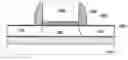
FIG. 1 is a cross-sectional view of a Ge-on-insulator structure according to an embodiment of the present disclosure; and
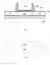
FIGS. 2-6 are cross-sectional diagrams of intermediate statuses of a Ge-on-insulator structure formed during a process of a method for forming the Ge-on-insulator structure according to an embodiment of the present disclosure.
DETAILED DESCRIPTION
Embodiments of the present disclosure will be described in detail in the following descriptions, examples of which are shown in the accompanying drawings, in which the same or similar elements and elements having same or similar functions are denoted by like reference numerals throughout the descriptions. The embodiments described herein with reference to the accompanying drawings are explanatory and illustrative, which are used to generally understand the present disclosure. The embodiments shall not be construed to limit the present disclosure.
Various embodiments and examples are provided in the following description to implement different structures of the present disclosure. In order to simplify the present disclosure, certain elements and settings will be described. However, these elements and settings are only examples and are not intended to limit the present disclosure. In addition, reference numerals may be repeated in different examples in the disclosure. This repeating is for the purpose of simplification and clarity and does not refer to relations between different embodiments and/or settings. Furthermore, examples of different processes and materials are provided in the present disclosure. However, it would be appreciated by those skilled in the art that other processes and/or materials may be also applied. Moreover, a structure in which a first feature is “on” a second feature may include an embodiment in which the first feature directly contacts the second feature and may include an embodiment in which an additional feature is prepared between the first feature and the second feature so that the first feature does not directly contact the second feature.
FIG. 1 is a cross-sectional view of a Ge-on-insulator structure according to an embodiment of the present disclosure. The GeOI structure comprises a silicon substrate 1100, on a surface of which an oxide insulating layer is formed; and a Ge layer 1200 formed on the silicon substrate 1100, in which a first semiconducting metal-germanide passivation layer 1300 is formed between the Ge layer 1200 and the silicon substrate 1100. In some embodiments, the first semiconducting metal-germanide passivation layer 1300 is a strontium germanide layer, a barium germanide layer or a stannum germanide layer formed by treating a first surface of the Ge layer 1200 using strontium, barium or stannum. In one embodiment, the first semiconducting metal-germanide passivation layer 1300 is bonded with the silicon substrate 1100. In one embodiment, the silicon substrate 1100 comprises a Si substrate and a SiO2 insulating layer formed on the Si substrate. In another embodiment, the Ge layer 1200 is a strained Ge layer, a strained Ge1-ySiy layer, a relaxed Ge layer or a relaxed Ge1-ySiy layer and y is within a range from 0 to 1. Because the strontium germanide layer, the barium germanide layer or the stannum germanide layer is a semiconductor layer, an interface state between Ge materials and an insulation oxide may be alleviated so as to reduce a leakage and a scattering at the interface, and a mobility of the Ge materials may not be reduced largely.
In one embodiment, the GeOI structure further comprises a second semiconducting metal-germanide passivation layer 1400 formed on the Ge layer 1200. Similarly, in some embodiments, the second semiconducting metal-germanide passivation layer 1400 is a strontium germanide layer, a barium germanide layer or a stannum germanide layer formed by treating a second surface of the Ge layer 1200 using strontium, barium or stannum. In other embodiments, the second semiconducting metal-germanide passivation layer 1400 may also be formed by other methods, that is, the second semiconducting metal-germanide passivation layer 1400 may be a Ge1-xSix layer and x is within a range from 0 to 1.
In one embodiment, the GeOI structure further comprises a gate dielectric layer 1500 formed on the second semiconducting metal-germanide passivation layer 1400, a gate electrode 1600 formed on the gate dielectric layer 1500, and a source 1700 and a drain 1700 formed in the Ge layer 1200.
FIGS. 2-6 are cross-sectional diagrams of intermediate statuses of a Ge-on-insulator structure formed during a process of a method for forming the Ge-on-insulator structure according to an embodiment of the present disclosure. The method comprises the following steps.
Step S101, a substrate 2000 is provided. In some embodiments, the substrate 2000 is a Si substrate or a Ge substrate. In other embodiments, other substrates may also be used. In some embodiments, the substrate 2000 may be reused, thus reducing a fabrication cost.
Step S102, a Ge layer 1200 is formed on the substrate 2000, as shown in FIG. 2. In one embodiment, the Ge layer 1200 may be a strained Ge layer, a strained Ge1-ySiy layer, a relaxed Ge layer or a relaxed Ge1-ySiy layer and y is within a range from 0 to 1.
Step S103, a first surface of the Ge layer 1200 is treated to form a first semiconducting metal-germanide passivation layer 1300, as shown in FIG. 3. In some embodiments, the first semiconducting metal-germanide passivation layer 1300 is a strontium germanide layer, a barium germanide layer or a stannum germanide layer.
Step S104, the first semiconducting metal-germanide passivation layer 1300 is connected with a silicon substrate 1100, on a surface of which an oxide insulating layer is formed, as shown in FIG. 4. In one embodiment, the first semiconducting metal-germanide passivation layer 1300 is bonded with the silicon substrate 1100.
Step S105, the substrate 2000 is removed, as shown in FIG. 5.
Step S106, a second surface of the Ge layer 1200 is treated to form a second semiconducting metal-germanide passivation layer 1400, as shown in FIG. 6. The second semiconducting metal-germanide passivation layer 1400 may be a strontium germanide layer, a barium germanide layer or a stannum germanide layer. Similarly, in other embodiments, the second semiconducting metal-germanide passivation layer 1400 may also be formed by other methods, that is, the second semiconducting metal-germanide passivation layer 1400 may be a Ge1-xSix layer and x is within a range from 0 to 1.
Step S107, a gate dielectric layer 1500 is formed on the second semiconducting metal-germanide passivation layer 1400, a gate electrode 1600 is formed on the gate dielectric layer 1500, and a source 1700 and a drain 1700 are formed in the Ge layer 1200, as shown in FIG. 1.
According to an embodiment of the present disclosure, because the strontium germanide layer, the barium germanide layer or the stannum germanide layer is a semiconductor layer, an interface state between Ge materials and an insulation oxide may be alleviated so as to reduce a leakage and a scattering at the interface, and a mobility of the Ge materials may not be reduced largely.
Although explanatory embodiments have been shown and described, it would be appreciated by those skilled in the art that changes, alternatives, and modifications all falling into the scope of the claims and their equivalents may be made in the embodiments without departing from spirit and principles of the disclosure.
Claims
What is claimed is:1. A method for forming a Ge-on-insulator structure, comprising steps of:
forming a Ge layer on a substrate;
treating a first surface of the Ge layer to form a first semiconducting metal-germanide passivation layer;
bonding the first semiconducting metal-germanide passivation layer with a silicon substrate, wherein on a surface of the silicon substrate an oxide insulating layer is formed; and
removing the substrate.
2. The method according to claim 1, further comprising:
after the substrate is removed, treating a second surface of the Ge layer to form a second semiconducting metal-germanide passivation layer.
3. The method according to claim 2, further comprising:
forming a gate dielectric layer on the second semiconducting metal-germanide passivation layer;
forming a gate electrode on the gate dielectric layer; and
forming a source and a drain in the Ge layer.
4. The method according to claim 1, further comprising:
after the substrate is removed, treating a second surface of the Ge layer to form a Ge1-xSix passivation layer, wherein x is within a range from 0 to 1.
5. The method according to claim 1, wherein the metal is at least one metal selected from a group consisting of strontium, barium or stannum.
6. The method according to claim 2, wherein the metal is at least one metal selected from a group consisting of strontium, barium or stannum.
7. The method according to claim 1, wherein the Ge layer is a strained Ge layer, a strained Ge1-ySiy layer, a relaxed Ge layer or a relaxed Ge1-ySiy layer, wherein y is within a range from 0 to 1.
8. A Ge-on-insulator structure, comprising:
a silicon substrate, wherein on a surface of the silicon substrate an oxide insulating layer is formed; and
a Ge layer formed on the silicon substrate,
wherein a first semiconducting metal-germanide passivation layer is formed between the Ge layer and the silicon substrate.
9. The Ge-on-insulator structure according to claim 8, further comprising:
a second semiconducting metal-germanide passivation layer formed on the Ge layer.
10. The Ge-on-insulator structure according to claim 9, further comprising:
a gate dielectric layer formed on the second semiconducting metal-germanide passivation layer,
a gate electrode formed on the gate dielectric layer; and
a source and a drain formed in the Ge layer.
11. The Ge-on-insulator structure according to claim 8, further comprising:
a Ge1-xSix passivation layer formed on the Ge layer, wherein x is within a range from 0 to 1.
12. The Ge-on-insulator structure according to claim 8, wherein the metal is at least one metal selected from a group consisting of strontium, barium or stannum.
13. The Ge-on-insulator structure according to claim 9, wherein the metal is at least one metal selected from a group consisting of strontium, barium or stannum.
14. The Ge-on-insulator structure according to claim 8, wherein the Ge layer is a strained Ge layer, a strained Ge1-ySiy layer, a relaxed Ge layer or a relaxed Ge1-ySiy layer, wherein y is within a range from 0 to 1.
Images & Drawings included:
Sources:
- United States Patent and Trademark Office - verify current appl. status at the USPTO↗
Similar patent applications:
Recent applications in this class:
- » 20240136441 2024-04-25
SEMICONDUCTOR DEVICE AND MEHTOD OF FABRICATING THE SAME - » 20230352597 2023-11-02
BIOSENSOR - » 20210408298 2021-12-30
SEMICONDUCTOR DEVICE AND METHOD FOR MANUFACTURING SEMICONDUCTOR DEVICE - » 20210376160 2021-12-02
Method of manufacturing a thin film transistor - » 20210226068 2021-07-22
Thin-film transistor and manufacturing method thereof - » 20200220025 2020-07-09
Thin film transistor and method for fabricating same - » 20200194596 2020-06-18
THIN FILM TRANSISTOR COMPRISING TWO DIMENSIONAL MATERIAL, DISPLAY COMPRISING THE SAME AND MANUFACTURING METHOD FOR THE SAME - » 20190013410 2019-01-10
Array substrate and display panel - » 20180331231 2018-11-15
Field-effect transistor and the manufacturing method - » 20170186881 2017-06-29
Carbon nanostructure device fabrication utilizing protect layers
Recent applications for this Assignee:
- » 20250263696 2025-08-21
PROTEIN TRANSLATION SYSTEM - » 20250255183 2025-08-07
ORGANIC LIGHT-EMITTING DIODE AND DISPLAY APPARATUS - » 20250255091 2025-08-07
ORGANIC LIGHT-EMITTING DIODE AND DISPLAY APPARATUS - » 20250239854 2025-07-24
Grid-Forming Control Method with Full-State Virtual Oscillator for Photovoltaic and Energy Storage SYSTEM, and Device - » 20250233215 2025-07-17
WATER AND ACID ADSORBING BATTERY SEPARATOR AND PREPARATION METHOD THEREFOR, WATER AND ACID ADSORBING ELECTRODE PLATE, AND BATTERY - » 20250232886 2025-07-17
POWER SUPPLY MODULE AND POWER SUPPLY SYSTEM - » 20250202515 2025-06-19
SINGLE-SIDEBAND PHASE-SENSITIVE DETECTION METHOD AND SYSTEM - » 20250150619 2025-05-08
DATA STORAGE METHOD, READING METHOD, APPARATUS, STORAGE MEDIUM, AND PROGRAM PRODUCT - » 20250149667 2025-05-08
METHOD OF TARGETED RECYCLING OF WASTE BATTERIES - » 20250133304 2025-04-24
EVENT DATA PROCESSING METHOD AND RELATED DEVICE