Optical touch panel and light guide module thereof
US20120206409A1
2012-08-16
13/096,789
2011-04-28
✅ Patent granted
US 8,913,035 B2
2014-12-16
-
-
Jesus Hernandez
Morris Manning & Martin LLP | Tim Tingkang Xia, Esq.
2033-09-20
Abstract:
An optical touch panel includes a panel and a light guide module. The light guide module is disposed on the panel, and the light guide module includes a printed circuit board, at least one light emitting element, and a light guide strip. The light emitting element is electrically disposed on the printed circuit board. The light guide strip is disposed on the printed circuit board, and wraps the light emitting element. Additionally, the light emitting element emits light rays, and the light rays penetrate the light guide strip and are emitted to the panel.
Inventors:
- Hui-Hsuan CHEN 2 🇹🇼 Hsinchu County, Taiwan
- Hung-Ching Lai 1 🇹🇼 Hsinchu County, Taiwan
- Kuo-Hsiung Li 1 🇹🇼 Hsinchu County, Taiwan
Assignee:
- PIXART IMAGING INC. 17 🇹🇼 Hsinchu County, Taiwan
Applicant:
Interested in similar patents?
Get notified when new applications in this technology area are published.
Classification:
G06F3/0421 » CPC further
Input arrangements for transferring data to be processed into a form capable of being handled by the computer; Output arrangements for transferring data from processing unit to output unit, e.g. interface arrangements; Input arrangements or combined input and output arrangements for interaction between user and computer; Arrangements for converting the position or the displacement of a member into a coded form; Digitisers, e.g. for touch screens or touch pads, characterised by the transducing means by opto-electronic means by interrupting or reflecting a light beam, e.g. optical touch-screen
H01L2924/0002 » CPC further
Indexing scheme for arrangements or methods for connecting or disconnecting semiconductor or solid-state bodies as covered by; Technical content checked by a classifier Not covered by any one of groups , and
H01L2924/00 » CPC further
Indexing scheme for arrangements or methods for connecting or disconnecting semiconductor or solid-state bodies as covered by
H01L33/02 IPC
Semiconductor devices with at least one potential-jump barrier or surface barrier specially adapted for light emission; Processes or apparatus specially adapted for the manufacture or treatment thereof or of parts thereof; Details thereof characterised by the semiconductor bodies
G02B6/00 IPC
Light guides
G02B6/001 » CPC main
Light guides specially adapted for lighting devices or systems the light guides being of the fibre type the light being emitted along at least a portion of the lateral surface of the fibre
H01L25/0753 » CPC further
Assemblies consisting of a plurality of individual semiconductor or other solid state devices ; Multistep manufacturing processes thereof all the devices being of a type provided for in the same subgroup of groups - , e.g. assemblies of rectifier diodes the devices not having separate containers the devices being of a type provided for in group the devices being arranged next to each other
G02B6/0073 » CPC further
Light guides specially adapted for lighting devices or systems the light guides being planar or of plate-like form characterised by the light source being coupled to the light guide Light emitting diode [LED]
G02B6/0021 » CPC further
Light guides specially adapted for lighting devices or systems the light guides being planar or of plate-like form; Means for improving the coupling-in of light from the light source into the light guide provided on the surface of the light guide or in the bulk of it by shaping at least a portion of the light guide, e.g. with collimating, focussing or diverging surfaces for housing at least a part of the light source, e.g. by forming holes or recesses
G02B6/0068 » CPC further
Light guides specially adapted for lighting devices or systems the light guides being planar or of plate-like form characterised by the light source being coupled to the light guide Arrangements of plural sources, e.g. multi-colour light sources
G06F3/042 IPC
Input arrangements for transferring data to be processed into a form capable of being handled by the computer; Output arrangements for transferring data from processing unit to output unit, e.g. interface arrangements; Input arrangements or combined input and output arrangements for interaction between user and computer; Arrangements for converting the position or the displacement of a member into a coded form; Digitisers, e.g. for touch screens or touch pads, characterised by the transducing means by opto-electronic means
H01L25/075 IPC
Assemblies consisting of a plurality of individual semiconductor or other solid state devices ; Multistep manufacturing processes thereof all the devices being of a type provided for in the same subgroup of groups - , e.g. assemblies of rectifier diodes the devices not having separate containers the devices being of a type provided for in group
Description
CROSS-REFERENCE TO RELATED APPLICATIONS
This non-provisional application claims priority under 35 U.S.C. §119(a) on Patent Application No. 100104651 filed in Taiwan, R.O.C. on Feb. 11, 2011, the entire contents of which are hereby incorporated by reference.
BACKGROUND OF THE INVENTION
1. Field of the Invention
The present invention relates to an optical touch panel, and more particularly to an optical touch panel having a light guide module.
2. Related Art
In recent years, a previous input manner of pressing a mechanical button begins to be replaced with an input manner in which a screen is contacted with an object or a finger. When a user contacts an image on the screen, a tactile feedback system on the screen may convert detected light ray data into an electronic signal and transfer the electronic signal to a processor, and the processor drives various electronic devices with a pre-programmed program, and thus vivid video and audio effects are presented through a screen picture.
A conventional tactile feedback system comprises a glass substrate, a Light Emitting Diode (LED), a photo-sensitive element, a lens, a reflecting element, and a light guide element. The photo-sensitive element, the LED and the lens are configured at an upper right corner of the glass substrate, and the reflecting sheet and the light guide element are simultaneously disposed at left and lower devices of the glass substrate.
The optical touch principle is to illuminate a distal reflecting component by a light emitting device, and when the finger or the contact object shields light rays, the photo-sensitive element may convert sensed and collected light ray changes into an electronic signal, and transfer the electronic signal to the processor to calculate a relative position of the finger or the contact object on the glass substrate. In order to enable the processor to precisely calculate the position of the finger on the glass substrate, internal components of an optical touch screen all need to be aligned repetitively and precisely. However, the number of the internal components of the optical touch screen in the prior art is excessively large, so the optical touch screen in the prior art is confronted with a complicated alignment problem.
Furthermore, the conventional optical touch screen reflects the light rays emitted by the light emitting device with the reflecting element to detect the relative position of the finger or the contact object on the glass substrate, so when the photo-sensitive element is receiving the light rays reflected by the reflecting element, a signal output by the photo-sensitive element is easily influenced by a surrounding light source. Likewise, the light rays reflected by the reflecting component and the light rays emitted by the light emitting device generate interference on the photo-sensitive element, thereby influencing the precision of sensing the light rays by the photo-sensitive element. Additionally, the light emitting device placed at the upper right corner of the glass substrate must illuminate the distal reflecting element, so a light emitting element of the optical touch screen in the prior art needs large brightness output and current input.
SUMMARY OF THE INVENTION
Accordingly, the present invention is an optical touch panel and a light guide module thereof, thereby solving problems in the prior art that large brightness output and current output are needed and repetitive and precise alignment is required during assembling.
The optical touch panel according to the present invention comprises a panel, a sensing element, and a light guide module. The panel has a touch area, and the light guide module is disposed on the panel. Moreover, the light guide module comprises a printed circuit board, at least one light emitting element, and a light guide strip. The light emitting element is electrically disposed on the printed circuit board, and emits light rays. The light guide strip is disposed on the printed circuit board, and wraps the light emitting element. The light guide strip has a first surface and the light rays are emitted out from the first surface, and the first surface is a light transmissive surface. The sensing element is disposed on the panel and located out of the touch area, and the sensing element is used for sensing an image formed when the light rays are projected onto an object.
The light guide module according to the present invention comprises a printed circuit board, a plurality of light emitting elements, and light transmissive plastic. A contact surface of the printed circuit board is rectangular, and the light emitting elements are electrically disposed on the contact surface of the printed circuit board. The light emitting elements are disposed on the contact surface along a long side of the contact surface at a predetermined interval. Finally, the light transmissive plastic is molded on the contact surface of the printed circuit board in a manner of extrusion molding or injection molding, and covers the light emitting elements.
In the optical touch panel according to the present invention, the light emitting element and the printed circuit board are integrated in a manner of extrusion molding or injection molding with the light transmissive plastic, so when the optical touch panel is assembled, it is only necessary to combine the light guide module with the printed circuit board, thereby replacing a method in which a light emitting device and a lens need to be assembled through an alignment reflecting element and a light guide element in the prior art. Therefore, compared with the prior art, the optical touch panel according to the present invention is capable of omitting a complicated alignment process, thereby saving assembling time of the optical touch panel.
In the optical touch panel according to the present invention, light rays are emitted out with a plurality of light emitting elements, and a uniform effect is generated, so as to solve a problem in the prior art that light rays generated by a light emitting device through a lens, a reflecting element and a light guide element are interfered with each other. Therefore, the optical touch panel according to the present invention is capable of reducing brightness needed by the light emitting element, thereby reducing brightness output and current input of the light emitting element.
These and other aspects of the present invention will become apparent from the following description of the preferred embodiment taken in conjunction with the following drawings, although variations and modifications therein may be affected without departing from the spirit and scope of the novel concepts of the disclosure.
BRIEF DESCRIPTION OF THE DRAWINGS
The accompanying drawings illustrate one or more embodiments of the invention and, together with the written description, serve to explain the principles of the invention. Wherever possible, the same reference numbers are used throughout the drawings to refer to the same or like elements of an embodiment, and wherein:
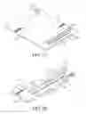
FIG. 1A is a schematic three-dimensional view of an optical touch panel according to a first embodiment of the present invention;
FIG. 1B is a schematic enlarged view of a light guide module in FIG. 1A;
FIG. 1C is a schematic plane view of the light guide module in FIG. 1A;
FIG. 2A is a schematic view showing a light ray emission direction of a direct-light LED according to the first embodiment of the present invention;
FIG. 2B is a schematic view showing a light ray emission direction of a direct-light LED according to the first embodiment of the present invention;
FIG. 3 is a schematic view showing a light ray emission direction of a side-light LED according to the first embodiment of the present invention;
FIGS. 4 and 5 are schematic enlarged views of a light guide strip according to the first embodiment of the present invention;
FIGS. 6A, 6B and 6C are schematic assembly views of the optical touch panel according to the first embodiment of the present invention;
FIG. 7A is a schematic three-dimensional view of an optical touch panel according to a second embodiment of the present invention; and
FIG. 7B is a schematic enlarged view of a light guide module in FIG. 7A.
DETAILED DESCRIPTION OF THE INVENTION
In an optical touch panel and a light guide module thereof according to the present invention, the mentioned light emitting element is a component mounted in the optical touch panel, the mentioned light emitting element comprises, but not limited to, a direct-light LED, a side-light LED, or a Cold Cathode Fluorescence Lamp (CCFL), but in the following specific embodiment of the present invention, the direct-light LED is used as an embodiment of the present invention.
FIG. 1 is a schematic three-dimensional view of a first embodiment according to the present invention, FIG. 1B is a schematic enlarged view of a light guide module in FIG. 1A, and FIG. 1C is a schematic plane view of the light guide module in FIG. 1A.
Referring to FIG. 1A, the optical touch panel according to the present invention comprises a panel 100, a sensing element 300, and a light guide module 200. The panel 100 is a transparent flat panel of an optical touch screen, and has a touch area 110. The light guide module 200 is disposed at a side edge of the panel 100 and located out of the touch area 110, and emits light rays to the touch area 110. The sensing element 300 is disposed on the panel 100 and located at a corner out of the touch area 110, and the sensing element 300 is used for sensing an image formed when the light rays are projected onto an object.
In this embodiment, the sensing element 300 is disposed at a corner out of the touch area 110, but the present invention is not limited to this, and for design needs, persons skilled in the art may further dispose the sensing element 300 at any position out of the touch area 110, such as at a side edge or a bottom edge.
The light guide module 200 is illustrated in detail hereinafter. Simultaneously referring to FIGS. 1A to 1C, the light guide module 200 according to the present invention comprises a printed circuit board 210, a light emitting element 220, and a light guide strip 230. For example, the printed circuit board 210 is in a strip shape, and the light emitting element 220 is an LED.
FIG. 2A is a schematic three-dimensional view showing a light ray emission direction of a direct-light LED, and FIG. 2B is a schematic three-dimensional view of the direct-light LED in FIG. 2A with a metal contact added. Continuously referring to FIGS. 2A and 2B, the light emitting element 220 protrudes on the printed circuit board 210, the light emitting element 220 has a top surface 223 and a first lateral surface 222, and the light emitting element 220 is electrically disposed on the printed circuit board 210 through a metal contact 221 of the top surface 223, so as to enable the light emitting element 220 to obtain supplies of a power supply through the printed circuit board 210. The light emitting element 220 is a direct-light LED 400, a majority of the light rays thereof is mainly emitted out from the top surface 223, and a part of the light rays is emitted from a lateral surface, so in order to enable light rays to be emitted out from a main light exit surface (the first lateral surface 222), in this embodiment, the area of the metal contact 221 is enlarged, so as to mask light rays emitted by the light emitting element 220 from the top surface 223.
Referring to FIG. 3, FIG. 3 is a schematic three-dimensional view showing a light ray emission direction of a side-light LED. In order to more effectively utilize the light source of the LED, in other embodiments according to the present invention, the LED may be changed into a side-light LED 410, and a light ray emission direction 224 thereof is mainly emitted out from a lateral surface of the LED, and is projected onto the touch area 110.
Referring to FIG. 4, the light guide strip 230 of the light guide module 200 according to the present invention wraps the light emitting element 220. The light guide strip is molded, for example, in an extrusion molding manner or an injection molding manner, and assumes a cuboid shape. A lateral surface facing the touch area 110 of the light guide strip 230 is a first surface 231, a third surface 233 is parallel to the first surface 231, and a second surface 232 connects upper surfaces of the first surface 231 and the third surface 233. In this embodiment, a light-proof surface 234 may also be added to the second surface 232 of the light guide strip 230, so as to mask the light rays emitted by the light emitting element 220 from the second surface 232, thereby avoiding causing light ray interference and influencing touch precision when the light rays are emitted to a non-touch area.
In order to enable the brightness of the optical touch panel 100 to be more uniform and to utilize the light source of the light emitting element 220 more appropriately, in the light guide module 200 according to the present invention, a reflecting component 235 may be further added to the second surface 232 or the third surface 233, or even reflecting components 235 are added to the second surface 232 and the third surface 233 simultaneously. Therefore, the light rays emitted to the second surface 232 or the third surface 233 are reflected onto other surfaces due to being irradiated to the reflecting component 235, so as to increase the probability of the light rays being emitted out from the first surface 231, thereby increasing the brightness and uniformity of the optical touch panel.
Referring to FIG. 5, in the light guide module 200 according to the present invention, in order to enable the brightness of the optical touch panel to be more uniform and to utilize the light source of the light emitting element 220 more appropriately, a pattern 236 may be further added to the third surface 233 of the light guide strip 230, so as to enable the light rays to be irregularly reflected at the time of passing through the third surface 233.
The light guide strip 230 of the optical touch panel according to the present invention wraps the light emitting element 220 in the extrusion molding manner or the injection molding manner, so compared with the prior art, in the present invention, a light emitting element and a light guide strip of a conventional optical touch screen are integrated into a single light guide module 200, thereby reducing assembling steps of the optical touch panel. The assembling of the optical touch panel is illustrated hereinafter. Referring to FIGS. 6A to 6C, a modular light guide module 200 is directly disposed at a side edge of the panel 100, and the sensing element 300 is disposed on the panel 100 and is located at a corner of the touch area 110.
In order to make the brightness of the optical touch screen more uniform, referring to FIGS. 7A and 7B, FIG. 7A is a schematic three-dimensional view of an optical touch panel according to a second embodiment of the present invention, and FIG. 7B is a schematic enlarged view of a light guide module in FIG. 7A. In the light guide module 200 according to the present invention, the printed circuit board 210 further has a plurality of light emitting elements 220 disposed thereon. The contact surface between the printed circuit board 210 and the light emitting element 220 is rectangular. The light emitting elements 220 are electrically disposed on the contact surface of the printed circuit board 210, and the light emitting elements 220 are disposed on the contact surface along a long side of the contact surface at a predetermined interval. A light transmissive plastic 240 is molded above the contact surface of the printed circuit board 210 in a manner of extrusion molding or injection molding, and covers the light emitting elements 220. The light transmissive plastic 240 is the light guide strip 230.
The light guide strip 230 of the optical touch panel according to the present invention wraps the light emitting elements 220 and the reflecting component 235 in the extrusion pressing molding manner or the injection molding manner, in which the reflecting component 235 may also be attached to an external surface of the light guide strip 230, so compared with the prior art, in the present invention, three internal components comprising an LED, a light guide element and a reflecting sheet of a conventional optical touch screen are integrated into a single light guide module 200, thereby shortening assembling time of the optical touch panel.
Additionally, the reflecting sheet is assembled in the light guide module 200, so interference of the light rays is performed in the light guide module 200, and then the light rays are projected onto the touch area 110, so as to solve the problem that the interference of the light rays is generated in the touch area 110 to cause redundant light rays to be projected into a photo-sensitive element, thereby reducing touch precision in the prior art. Likewise, in the optical touch panel according to the present invention, the reflecting component 235 makes the brightness of the optical touch panel more uniform.
Moreover, a plurality of light emitting elements 220 of the optical touch panel according to the present invention is distributed on the printed circuit board 210 at a predetermined interval, so besides being capable of increasing the brightness of the optical touch panel due to the increased number of the light emitting elements 220, the uniformity of the optical touch panel may also be increased since the light rays are emitted into the touch area 110 from different angles.
Claims
What is claimed is:1. An optical touch panel, comprising:
a panel, having a touch area;
a light guide module, disposed on the panel, and the light guide module comprising:
a printed circuit board;
at least one light emitting element, electrically disposed on the printed circuit board, wherein the light emitting element emits light rays; and
a light guide strip, disposed on the printed circuit board, wrapping the light emitting element, and having a first surface, wherein the first surface is a light transmissive surface and the light rays are emitted out from the first surface; and
a sensing element, disposed on the panel and located out of the touch area, wherein the sensing element is used for sensing an image formed when the light rays are projected onto an object.
2. The optical touch panel according to claim 1, wherein the light guide strip wraps the light emitting element in a manner of extrusion molding or injection molding.
3. The optical touch panel according to claim 1, wherein the light guide strip further has a second surface and a third surface, the third surface is parallel to the first surface, and the second surface is connected between the first surface and the third surface.
4. The optical touch panel according to claim 3, wherein the second surface and/or the third surface has a reflecting component.
5. The optical touch panel according to claim 3, wherein the third surface of the light guide strip has a pattern, so that the light rays are irregularly reflected on the third surface.
6. The optical touch panel according to claim 3, wherein the light emitting element is a direct-light Light Emitting Diode (LED), each of the light emitting elements faces an upper surface of the second surface, and the upper surface is a light-proof surface, thereby masking the light rays emitted towards the second surface.
7. The optical touch panel according to claim 6, wherein the upper surface of each of the light emitting elements is a metal contact of the light emitting element, and an area of the metal contact is approximately equal to an area of the upper surface, thereby masking the light rays emitted towards the second surface by the light emitting element.
8. The optical touch panel according to claim 1, wherein the light emitting element is a side-light LED, the light rays of the light emitting element is emitted out from a lateral surface, and the upper surface of the light emitting element does not emit the light rays.
9. The optical touch panel according to claim 1, further comprising a plurality of light emitting elements, the light emitting elements are electrically disposed on the printed circuit board, and the light emitting elements are arranged at an interval.
10. A light guide module, comprising:
a printed circuit board;
at least one light emitting element, electrically disposed on the printed circuit board, wherein the light emitting element emits light rays; and
a light guide strip, disposed on the printed circuit board, wrapping the light emitting element, and having a first surface, wherein the first surface is a light transmissive surface, and the light rays are emitted out from the first surface.
11. The light guide module according to claim 10, wherein the light guide strip wraps the light emitting element in a manner of extrusion molding or injection molding.
12. The light guide module according to claim 10, wherein the light guide strip further has a second surface and a third surface, the third surface is parallel to the first surface, and the second surface is connected between the first surface and the third surface.
13. The light guide module according to claim 12, wherein the second surface and/or the third surface has a reflecting component.
14. The light guide module according to claim 12, wherein the third surface of the light guide strip has a pattern, so that the light rays are irregularly reflected on the third surface.
15. The light guide module according to claim 12, wherein the light emitting element is a direct-light Light Emitting Diode (LED), and an upper surface of each of the light emitting elements facing the second surface is a light-proof surface, thereby masking the light rays emitted towards the second surface.
16. The light guide module according to claim 15, wherein the upper surface of each of the light emitting elements is a metal contact of the light emitting element, and an area of the metal contact is approximately equal to an area of the upper surface, thereby masking the light rays emitted by the light emitting element towards the second surface.
17. The light guide module according to claim 10, wherein the light emitting element is a side-light LED, the light rays of the light emitting element are emitted out from a lateral surface, and the upper surface of the light emitting element does not emit the light rays.
18. The light guide module according to claim 10, further comprising a plurality of light emitting elements, the light emitting elements are electrically disposed on the printed circuit board, and the light emitting elements are arranged at an interval.
19. A light guide module, comprising:
a printed circuit board, wherein a contact surface of the printed circuit board is rectangular;
a plurality of light emitting elements, electrically disposed on the contact surface of the printed circuit board, wherein the light emitting elements are disposed on the contact surface along a long side of the contact surface at a predetermined interval; and
a light transmissive plastic, molded above the contact surface of the printed circuit board in a manner of extrusion molding or injection molding, and covering the light emitting elements.
20. The light guide module according to claim 19, wherein the light transmissive plastic further has a second surface and a third surface, the third surface is parallel to a first surface, and the second surface is connected between the first surface and the third surface.
21. The light guide module according to claim 20, wherein the second surface and/or the third surface has a reflecting component.
22. The light guide module according to claim 20, wherein the third surface of the light transmissive plastic has a pattern, so that the light rays are irregularly reflected on the third surface.
23. The light guide module according to claim 20, wherein the light emitting elements are direct-light Light Emitting Diodes (LEDs), and an upper surface of each of the light emitting elements facing the second surface is a light-proof surface, thereby masking the light rays emitted towards the second surface.
24. The light guide module according to claim 23, wherein the upper surface of each of the light emitting elements is a metal contact of the light emitting elements, and an area of the metal contact is approximately equal to an area of the upper surface, thereby masking the light rays emitted by the light emitting elements towards the second surface.
25. The light guide module according to claim 19, wherein the light emitting elements are side-light LEDs, the light rays of the light emitting elements are emitted out by a lateral surface, and an upper surface of the light emitting elements does not emit the light rays.
Images & Drawings included:


Sources:
- United States Patent and Trademark Office - verify current appl. status at the USPTO↗
Recent applications in this class:
- » 20250277927 2025-09-04
PERIPHERAL LIGHT-EMITTING LINEAR LIGHT GUIDE MEMBER AND METHOD OF MANUFACTURING THE SAME - » 20250244516 2025-07-31
OPTICAL WAVEGUIDE-BASED SIDE ILLUMINATING ASSEMBLY, ELONGATED REINFORCING STRUCTURE, AND RECEPTACLE - » 20250244515 2025-07-31
Light Pipe Lighting Apparatus - » 20250199228 2025-06-19
LASER LIGHTING SYSTEM COMPRISING OPTICAL FIBER - » 20250076557 2025-03-06
DISPLAY SYSTEMS INCLUDING PHOTONIC INTEGRATED CIRCUITS - » 20240248246 2024-07-25
Cooking Appliance Light - » 20240248245 2024-07-25
Low-profile color-mixing lightpipe - » 20240192422 2024-06-13
METHOD FOR PREPARING OPTICAL FIBRES WITH LATERAL LIGHT EMISSION AND INSTALLATION FOR IMPLEMENTING SAME - » 20240176057 2024-05-30
PERIPHERAL SURFACE-EMITTING LINEAR LIGHT GUIDE AND METHOD FOR MANUFACTURING THE SAME - » 20240061164 2024-02-22
Lace fabric of helical structure containing twisted optical fiber threads and production method therefor
Recent applications for this Assignee:
- » 20180063604 2018-03-01
Signal sending device, signal receiving device, and signal sending and receiving system and method - » 20130300713 2013-11-14
Power saving sensing module for computer peripheral devices and method thereof - » 20130300663 2013-11-14
Power-saving sensing module for optical mouse and power-saving sensing method - » 20130300351 2013-11-14
WIRELESS TRANSCEIVER AND WIRELESS TRANSCEIVER SYSTEM - » 20130044380 2013-02-21
LENS MODULE AND METHOD FOR MANUFACTURING THE SAME - » 20120249293 2012-10-04
Recognition system and recognition method - » 20120212452 2012-08-23
Method for detecting object on an operation interface of a touchable device and touchable device using the same - » 20120205166 2012-08-16
Sensing system - » 20120155388 2012-06-21
Signal sending device, signal receiving device, and signal sending and receiving system and method - » 20120120024 2012-05-17
TOUCH SYSTEM AND OPTICAL TOUCH SYSTEM WITH POWER-SAVING MECHANISM