Memory testing system and method of computing device
US20120331345A1
2012-12-27
13/313,006
2011-12-07
✅ Patent granted
US 8,539,289 B2
2013-09-17
-
-
John Trimmings
Altis Law Group, Inc.
2032-02-10
Abstract:
In a memory testing method for testing a memory module of a computing device, an operating voltage of the memory module is adjusted to a first voltage or a second voltage. A predetermined data set is written into the memory module after the operating voltage of the memory module is adjusted, and the written data set is read out from the memory module, to accomplish a data writing and reading process of the memory module. A register value that presents how many memory errors have occurred during the data writing and reading process is acquired from an ECC register of the memory module, to determine whether the memory module is stable during the adjusting of the operating voltage according to the register value.
Inventors:
- YU-LONG LIN 7 🇨🇳 Shenzhen City, China
- HUA DONG 8 🇨🇳 Shenzhen City, China
- JIE-JUN TAN 7 🇨🇳 Shenzhen City, China
- Hua Dong 8 🇨🇳 Shenzhen, China
- Yu-Long Lin 7 🇨🇳 Shenzhen, China
- Jie-Jun Tan 5 🇨🇳 Shenzhen, China
Assignee:
- HON HAI PRECISION INDUSTRY CO., LTD. 12,833 🇹🇼 Tu-Cheng, Taiwan
- HONG FU JIN PRECISION INDUSTRY (SHENZHEN) CO., LTD. 4,225 🇨🇳 Shenzhen City, China
- HON HAI PRECISION INDUSTRY CO., LTD. 10,014 🇹🇼 New Taipei, Taiwan
- HONG FU JIN PRECISION INDUSTRY (ShenZhen) CO., LTD. 2,585 🇨🇳 Shenzhen, China
Applicant:
Interested in similar patents?
Get notified when new applications in this technology area are published.
Classification:
G11C29/50 » CPC main
Checking stores for correct operation ; Subsequent repair ; Testing stores during standby or offline operation; Detection or location of defective memory elements, e.g. cell constructio details, timing of test signals Marginal testing, e.g. race, voltage or current testing
G11C29/021 » CPC further
Checking stores for correct operation ; Subsequent repair ; Testing stores during standby or offline operation; Detection or location of defective auxiliary circuits, e.g. defective refresh counters in voltage or current generators
G11C29/028 » CPC further
Checking stores for correct operation ; Subsequent repair ; Testing stores during standby or offline operation; Detection or location of defective auxiliary circuits, e.g. defective refresh counters with adaption or trimming of parameters
G11C2029/5004 » CPC further
Checking stores for correct operation ; Subsequent repair ; Testing stores during standby or offline operation; Detection or location of defective memory elements, e.g. cell constructio details, timing of test signals; Marginal testing, e.g. race, voltage or current testing Voltage
G06F11/26 IPC
Error detection; Error correction; Monitoring; Detection or location of defective computer hardware by testing during standby operation or during idle time, e.g. start-up testing Functional testing
G11C29/00 IPC
Checking stores for correct operation ; Subsequent repair ; Testing stores during standby or offline operation
Description
BACKGROUND
1. Technical Field
Embodiments of the present disclosure relate generally to memory testing technologies, and particularly to a memory testing system and method for testing an memory module of a computing device.
2. Description of Related Art
A memory error often occurs during data transmission of a memory module of a computing device. Since the memory error may cause the computing device to crash, it is necessary to test the memory module once the memory module has been installed in the computing device. In a typical memory module testing method, the memory module is tested based on a stable operating voltage. However, the operating voltage of the memory module may be changed due to some unexpected factors, such as a failure of a component of a motherboard. Therefore, a more efficient testing system and method is desired to detect whether the memory module is stable when the voltage of the memory module is changed.
BRIEF DESCRIPTION OF THE DRAWINGS
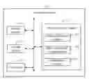
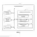
FIG. 1 is a schematic diagram illustrating one embodiment of a computing device comprising a memory testing system.
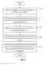
FIG. 2 is a flowchart of one embodiment of a memory testing method for testing a memory module of the computing device of FIG. 1.
DETAILED DESCRIPTION
The disclosure, including the accompanying drawings, is illustrated by way of example and not by way of limitation. It should be noted that references to “an” or “one” embodiment in this disclosure are not necessarily to the same embodiment, and such references mean at least one.
FIG. 1 is a schematic diagram illustrating one embodiment of a computing device 1 comprising a memory testing system 10 The computing device 1 further comprises a memory module 11, a storage system 12, and a processor 13. The memory testing system 10 tests the memory module 11 to detect whether the memory module 11 is stable by changing an operating voltage of the memory module 11. In one embodiment, the memory module 11 is an error checking and correcting (ECC) memory module that can automatically check and correct memory errors. It is understood that the memory module 11 can refer to one or more memory modules depending on the embodiment. It is further understood that FIG. 1 is only one example of the computing device 1 that can include more or fewer components than those shown in the embodiment, or a different configuration of the various components.
The storage system 12 stores one or more programs, such as programs of a firmware or other applications of the computing device 1 and executed by the processor 13 to provide functions of the computing device 1. In one embodiment, the storage system 12 may be a random access memory (RAM) for temporary storage of information, and/or a read only memory (ROM) for permanent storage of information. In other embodiments, the storage system 12 may also be an external storage device, such as a hard disk, a storage card, or a data storage medium.
The memory testing system 10 may include a plurality of software programs in the form of one or more computerized instructions stored in the storage system 12 and executed by the processor 13, to perform operations of the computing device 1. In the embodiment, the memory testing system 10 includes a voltage adjustment module 101, a data reading and writing module 102, and a determination module 103. In general, the word “module”, as used herein, refers to logic embodied in hardware or firmware, or to a collection of software instructions, written in a programming language, such as, Java, C, or assembly. One or more software instructions in the modules may be embedded in firmware, such as in an EPROM. The modules described herein may be implemented as either software and/or hardware modules and may be stored in any type of non-transitory computer-readable medium or other storage device. Some non-limiting examples of non-transitory computer-readable medium include CDs, DVDs, BLU-RAY, flash memory, and hard disk drives.
The voltage adjusting module 101 adjusts the operating voltage of the memory module 11 to a first voltage. In the embodiment, the operating voltage of the memory module is a stub series terminated logic (SSTL) voltage. The first voltage is V+ V, where the V is a nominal operating voltage or a standard operating voltage of the memory module 11, and the V is predetermined according to a range of the operating voltage of the memory module 11. For example, if the nominal operating voltage or the standard operating voltage V is 3.3V, and the range of the operating voltage is 3.3V 0.2V, the V can be predetermined as 0.1V.
The data reading and writing module 102 writes a predetermined data set into the memory module 11 after the operating voltage of the memory module 11 is adjusted to the first voltage, and reads out the written data set from the memory module 11, to accomplish a data writing and reading process of the memory module 11. In the embodiment, the memory module 11 may automatically check and correct memory errors (data errors) occurred in during the data writing and reading process using an ECC function of the memory module 11. If the memory errors are checked and are corrected, the memory module 11 may record how many memory errors are in an ECC register of the memory module 11.
The voltage adjustment module 101 further adjusts the operating voltage of the memory module 11 to a second value, where the second value is V− V.
The data reading and writing module 102 further writes the data set into the memory module 11 when the operating voltage of the memory module 11 is adjusted to the second voltage, and reads out the written data set from the memory module 11.
The determination module 103 acquires a register value of the ECC register of the memory module 11 after the data writing and reading process is accomplished under the second voltage, and determines whether the memory module 11 is stable during the changing of the operating voltage of the memory module 11 according to the register value. In the embodiment, the register value represents how many memory errors are in the memory module 11 during the data writing and reading process of the memory module 11. If the register value is equal to or less than a predefined value, such as a digital number “0”, the determination module 103 determines that the memory module 11 is stable because no memory errors occurred during the data writing and reading process. If the register value is greater than the predefined value “0”, the determination module 103 determines that the memory module 11 is unstable because one or more memory errors have occurred during the data writing and reading process. In addition, the determination module 103 further generates a test result indicating the amount of the memory errors that have occurred after the data writing and reading process is accomplished under the second voltage if the memory module 11 is determined to be unstable.
FIG. 2 is a flowchart of one embodiment of a memory testing method of the computing device 1 of FIG. 1. Depending on the embodiment, additional blocks may be added, others removed, and the ordering of the blocks may be changed.
In block SOL the voltage adjusting module 101 adjusts the operating voltage of the memory module 11 to a first voltage. In the embodiment, the operating voltage of the memory module is a stub series terminated logic (SSTL) voltage. The first voltage is V+ V, where V is a nominal operating voltage or a standard operating voltage of the memory module 11, V is predetermined according to a range of the operating voltage of the memory module 11. The operating voltage of the memory module 11 may be adjusted through a basic input output system (BIOS) of the computing device.
In block S02, the data reading and writing module 102 writes a predetermined data set into the memory module 11, and reads out the written data set from the memory module 11, to accomplish a data writing and reading process of the memory module 11.
In block S03, the voltage adjustment module 101 adjusts the operating voltage of the memory module 11 to a second value, where the second value is V− V.
In block S04, the data reading and writing module 102 writes the data set into the memory module 11, and reads out the written data set from the memory module 11.
In block S05, the determination module 103 acquires a register value of the ECC register of the memory module 11 after the data writing and reading process is accomplished under the second voltage, and determines whether the memory module 11 is stable during the changing of the operating voltage of the memory module 11 according to the register value. In addition, the determination module 103 further generates a test result indicating the amount of the memory errors that have occurred after the data writing and reading process is accomplished under the second voltage if the memory module 11 is determined to be unstable. In the embodiment, if the register value is equal to or less than a predefined value, such as a digital number “0”, the determination module 103 determines that the memory module 11 is stable because no memory error occurred during the data writing and reading process. If the register value is greater than the predefined value “0”, the determination module 103 determines that the memory module 11 is unstable because one or more memory errors have occurred during the data writing and reading process.
Although certain embodiments of the present disclosure have been specifically described, the present disclosure is not to be construed as being limited thereto. Various changes or modifications may be made to the present disclosure without departing from the scope and spirit of the present disclosure.
Claims
What is claimed is:1. A memory testing method for testing a memory module of a computing device, the method comprising:
adjusting an operating voltage of the memory module to a first voltage;
writing a predetermined data set into the memory module, and reading out the written data set from the memory module when the operating voltage of the memory module is adjusted to the first voltage, to accomplish a data writing and reading process of the memory module;
adjusting the operating voltage of the memory module to a second value;
writing the data set into the memory module, and reading out the written data set from the memory module when the operating voltage of the memory module is adjusted to the second value;
acquiring a register value of an error checking and correcting (ECC) register of the memory module after the data writing and reading process is accomplished under the second voltage;
determining whether the memory module is stable during the adjusting of the operating voltage of the memory module according to the register value; and
generating a test result indicating how many memory errors have occurred after the data writing and reading process is accomplished under the second voltage if the memory module is determined to be unstable.
2. The method according to claim 1, wherein the memory module is determined to be stable if the register value is equal to or less than a predefined value, and wherein the memory module is determined to be unstable if the register value is greater than the predefined value.
3. The method according to claim 1, wherein the first voltage is V+ V, and the second voltage is V− V, where the V is a nominal operating voltage or a standard operating voltage of the memory module, and the V is predetermined according to a range of the operating voltage of the memory module.
4. The method according to claim 1, wherein the operating voltage of the memory module is adjusted through a basic input output system (BIOS) of the computing device.
5. The method according to claim 1, wherein the memory module is an ECC memory module that automatically checks and corrects the memory errors occurred during the data writing and reading process using an ECC function.
6. The method according to claim 1, wherein the register value of the ECC register represents how many memory errors that have occurred during the data writing and reading process.
7. A computing device, comprising:
a memory module;
a storage system;
at least one processor;
one or more programs stored in the storage system and being executable by the at least one processor, the one or more programs comprising:
a voltage adjustment module operable to adjust an operating voltage of the memory module to a first voltage, and adjust the operating voltage of the memory module to a second voltage;
a data reading and writing module operable to write a predetermined data set into the memory module, and reading out the written data set from the memory module when the operating voltage of the memory module is adjusted, to accomplish a data writing and reading process of the memory module; and
a determination module operable to acquires a register value of an error checking and correcting (ECC) register of the memory module after the data writing and reading process is accomplished under the second voltage, and determine whether the memory module is stable during the adjusting of the operating voltage of the memory module according to the register value, and generate a test result indicating how many memory errors have occurred after the data writing and reading process is accomplished under the second voltage if the memory module is determined to be unstable.
8. The computing device according to claim 7, wherein the memory module is determined to be stable if the register value is equal to or less than a predefined value, and wherein the memory module is determined to be unstable if the register value is greater than the predefined value.
9. The computing device according to claim 7, wherein the first voltage is V+ V, and the second voltage is V− V, where the V is a nominal operating voltage or a standard operating voltage of the memory module, and the V is predetermined according to a range of the operating voltage of the memory module.
10. The computing device according to claim 7, wherein the operating voltage of the memory module is adjusted through a basic input output system (BIOS) of the computing device.
11. The computing device according to claim 7, wherein the memory module is an ECC memory module that automatically checks and corrects the memory errors that occurred during the data writing and reading process using an ECC function.
12. The computing device according to claim 7, wherein the register value of the ECC register represents how many memory errors have occurred during the data writing and reading process.
13. A non-transitory storage medium storing a set of instructions, the set of instructions capable of being executed by a processor of a computing device, cause the computing device to perform a memory testing method for testing a memory module of the computing device, the method comprising:
adjusting an operating voltage of the memory module to a first voltage;
writing a predetermined data set into the memory module, and reading out the written data set from the memory module when the operating voltage of the memory module is adjusted to the first voltage, to accomplish a data writing and reading process of the memory module;
adjusting the operating voltage of the memory module to a second value;
writing the data set into the memory module, and reading out the written data set from the memory module when the operating voltage of the memory module is adjusted to the second value;
acquiring a register value of an error checking and correcting (ECC) register of the memory module after the data writing and reading process is accomplished under the second voltage;
determining whether the memory module is stable during the adjusting of the operating voltage of the memory module according to the register value; and
generating a test result indicating how many memory errors have occurred after the data writing and reading process is accomplished under the second voltage if the memory module is determined to be unstable.
14. The non-transitory storage medium according to claim 13, wherein the memory module is determined to be stable if the register value is equal to or less than a predefined value, and wherein the memory module is determined to be unstable if the register value is greater than the predefined value.
15. The non-transitory storage medium according to claim 13, wherein the first voltage is V+ V, and the second voltage is V− V, where the V is a nominal operating voltage or a standard operating voltage of the memory module, and the V is a predetermined voltage value according to a range of the operating voltage of the memory module.
16. The non-transitory storage medium according to claim 13, wherein the operating voltage of the memory module is adjusted through a basic input output system (BIOS) of the computing device.
17. The non-transitory storage medium according to claim 13, wherein the memory module is an ECC memory module that automatically checks and corrects the memory errors that occurred during the data writing and reading process using an ECC function.
18. The non-transitory storage medium according to claim 13, wherein the register value of the ECC register represents how many memory errors have occurred during the data writing and reading process.
Images & Drawings included:
Sources:
- United States Patent and Trademark Office - verify current appl. status at the USPTO↗
Similar patent applications:
- » 20230187006
System and method of testing memory device and non-transitory computer readable medium - » 20060111889
Systems and methods for testing how computer systems interact with long-term memory storage devices - » 20160218802
METHOD AND SYSTEM FOR MEASURING AN OPTICAL POWER ATTENUATION VALUE OF A MULTIMODE DEVICE UNDER TEST, RECEIVE DEVICE AND COMPUTER-READABLE MEMORY - » 20160337034
Method and system for measuring an optical power attenuation value of a multimode device under test, receive device and computer-readable memory
Recent applications in this class:
- » 20250279151 2025-09-04
SELF-LEARNING BUILT-IN SELF-TEST (BIST) FOR LEAK DETECTION IN NON-VOLATILE MEMORY - » 20240282397 2024-08-22
Semiconductor memory apparatus and testing method thereof - » 20240233854 2024-07-11
SEMICONDUCTOR INTEGRATED CIRCUIT DEVICE - » 20240145024 2024-05-02
Test device and test method thereof - » 20240071551 2024-02-29
SEMICONDUCTOR STORAGE APPARATUS - » 20230377675 2023-11-23
Pulse detection in microelectronic devices, and related devices, systems, and methods - » 20230238075 2023-07-27
Read disturb information determination system - » 20230122275 2023-04-20
Voltage calibration scans to reduce memory device overhead - » 20230104520 2023-04-06
Semiconductor memory device with defect detection capability - » 20230093321 2023-03-23
Semiconductor devices and semiconductor systems for performing test
Recent applications for this Assignee:
- » 20250218287 2025-07-03
METHOD OF GENERATING AND PROMPTING TRAFFIC INFORMATION, AND ROADSIDE DEVICE THEREOF - » 20250178535 2025-06-05
METHOD FOR CONSTRUCTING 3D PANORAMIC VIEW MODEL, VEHICLE-MOUNTED DEVICE, AND STORAGE MEDIUM - » 20250074444 2025-03-06
METHOD FOR EARLY WARNING A BLIND AREA, ELECTRONIC DEVICE AND STORAGE MEDIUM - » 20240416754 2024-12-19
DISPLAY CONTROL DEVICE, DISPLAY EQUIPMENT, AND VEHICLE EMPLOYING DEVICE - » 20240411051 2024-12-12
Light-emitting device array and optical transceiver system having the same - » 20240324114 2024-09-26
DISPLAY CONTROL DEVICE AND VEHICLE EMPLOYING DEVICE - » 20240295957 2024-09-05
METHOD FOR CONTROLLING ELECTRONIC DEVICE, ELECTRONIC DEVICE AND COMPUTER STROAGE MEDIUM EMPLOYING METHOD - » 20240257357 2024-08-01
METHOD FOR DETECTING OBSTACLES, ELECTRONIC DEVICE, AND STORAGE MEDIUM - » 20240203133 2024-06-20
LANE LINE RECOGNITION METHOD, ELECTRONIC DEVICE AND STORAGE MEDIUM - » 20240194999 2024-06-13
Robot using limiting device for locking battery