Package substrate having die pad with outer raised portion and interior recessed portion
US20130001760A1
2013-01-03
13/175,587
2011-07-01
✅ Patent granted
US 8,455,989 B2
2013-06-04
-
-
David Vu | Brandon Fox
Steven A. Shaw | W. James Brady | Frederick J. Telecky, Jr.
2031-07-01
Abstract:
An electronic assembly includes a substrate including a die pad, where the die pad includes and an outer raised flat portion and a recessed portion that includes an inner recessed portion. A semiconductor die is directly on the outer raised flat portion and affixed to the die pad by a die attach material that is in the inner recessed portion. The die attach material is not on a top surface of the outer raised flat portion.
Inventors:
- CHIH-CHIEN HO 2 🇹🇼 TAIPEI, Taiwan
- SAIHSI JEN 2 🇹🇼 TAIPEI-HSIEN, Taiwan
- ERIC HSIEH 2 🇹🇼 TAIPEI-HSIEN, Taiwan
Assignee:
- TEXAS INSTRUMENTS INCORPORATED 18,931 🇺🇸 Dallas, TX, United States
Applicant:
Interested in similar patents?
Get notified when new applications in this technology area are published.
Classification:
H01L24/80 » CPC main
Arrangements for connecting or disconnecting semiconductor or solid-state bodies; Methods or apparatus related thereto Methods for connecting semiconductor or other solid state bodies using means for bonding being attached to, or being formed on, the surface to be connected
H01L23/49503 » CPC further
Details of semiconductor or other solid state devices; Arrangements for conducting electric current to or from the solid state body in operation, e.g. leads, terminal arrangements ; Selection of materials therefor consisting of soldered constructions; Lead-frames or other flat leads characterised by the die pad
H01L23/49513 » CPC further
Details of semiconductor or other solid state devices; Arrangements for conducting electric current to or from the solid state body in operation, e.g. leads, terminal arrangements ; Selection of materials therefor consisting of soldered constructions; Lead-frames or other flat leads characterised by the die pad having bonding material between chip and die pad
H01L23/498 » CPC further
Details of semiconductor or other solid state devices; Arrangements for conducting electric current to or from the solid state body in operation, e.g. leads, terminal arrangements ; Selection of materials therefor consisting of soldered constructions Leads, on insulating substrates,
H01L24/32 » CPC further
Arrangements for connecting or disconnecting semiconductor or solid-state bodies; Methods or apparatus related thereto; Means for bonding being attached to, or being formed on, the surface to be connected, e.g. chip-to-package, die-attach, "first-level" interconnects; Manufacturing methods related thereto; Layer connectors, e.g. plate connectors, solder or adhesive layers; Manufacturing methods related thereto; Structure, shape, material or disposition of the layer connectors after the connecting process of an individual layer connector
H01L24/97 » CPC further
Arrangements for connecting or disconnecting semiconductor or solid-state bodies; Methods or apparatus related thereto; Batch processes at chip-level, i.e. with connecting carried out on a plurality of singulated devices, i.e. on diced chips the devices being connected to a common substrate, e.g. interposer, said common substrate being separable into individual assemblies after connecting
H01L23/3107 » CPC further
Details of semiconductor or other solid state devices; Encapsulations, e.g. encapsulating layers, coatings, e.g. for protection characterised by the arrangement or shape the device being completely enclosed
H01L23/4985 » CPC further
Details of semiconductor or other solid state devices; Arrangements for conducting electric current to or from the solid state body in operation, e.g. leads, terminal arrangements ; Selection of materials therefor consisting of soldered constructions; Leads, on insulating substrates, Flexible insulating substrates
H01L24/48 » CPC further
Arrangements for connecting or disconnecting semiconductor or solid-state bodies; Methods or apparatus related thereto; Means for bonding being attached to, or being formed on, the surface to be connected, e.g. chip-to-package, die-attach, "first-level" interconnects; Manufacturing methods related thereto; Wire connectors; Manufacturing methods related thereto; Structure, shape, material or disposition of the wire connectors after the connecting process of an individual wire connector
H01L24/73 » CPC further
Arrangements for connecting or disconnecting semiconductor or solid-state bodies; Methods or apparatus related thereto Means for bonding being of different types provided for in two or more of groups , , , , , , ,
H01L2224/83192 » CPC further
Indexing scheme for arrangements for connecting or disconnecting semiconductor or solid-state bodies and methods related thereto as covered by; Methods for connecting semiconductor or other solid state bodies using means for bonding being attached to, or being formed on, the surface to be connected using a layer connector; Arrangement of the layer connectors prior to mounting wherein the layer connectors are disposed only on another item or body to be connected to the semiconductor or solid-state body
H01L2224/73204 » CPC further
Indexing scheme for arrangements for connecting or disconnecting semiconductor or solid-state bodies and methods related thereto as covered by; Means for bonding being of different types provided for in two or more of groups; Location after the connecting process on the same surface; Bump and layer connectors the bump connector being embedded into the layer connector
H01L2224/26175 » CPC further
Indexing scheme for arrangements for connecting or disconnecting semiconductor or solid-state bodies and methods related thereto as covered by; Means for bonding being attached to, or being formed on, the surface to be connected, e.g. chip-to-package, die-attach, "first-level" interconnects; Manufacturing methods related thereto; Layer connectors, e.g. plate connectors, solder or adhesive layers; Manufacturing methods related thereto; Auxiliary members for layer connectors, e.g. spacers being formed on an item to be connected not being a semiconductor or solid-state body Flow barriers
H01L2224/97 » CPC further
Indexing scheme for arrangements for connecting or disconnecting semiconductor or solid-state bodies and methods related thereto as covered by; Batch processes at chip-level, i.e. with connecting carried out on a plurality of singulated devices, i.e. on diced chips the devices being connected to a common substrate, e.g. interposer, said common substrate being separable into individual assemblies after connecting
H01L2924/00012 » CPC further
Indexing scheme for arrangements or methods for connecting or disconnecting semiconductor or solid-state bodies as covered by; Technical content checked by a classifier Relevant to the scope of the group, the symbol of which is combined with the symbol of this group
H01L2224/83385 » CPC further
Indexing scheme for arrangements for connecting or disconnecting semiconductor or solid-state bodies and methods related thereto as covered by; Methods for connecting semiconductor or other solid state bodies using means for bonding being attached to, or being formed on, the surface to be connected using a layer connector; Bonding interfaces outside the semiconductor or solid-state body Shape, e.g. interlocking features
H01L2924/00 » CPC further
Indexing scheme for arrangements or methods for connecting or disconnecting semiconductor or solid-state bodies as covered by
H01L2224/27013 » CPC further
Indexing scheme for arrangements for connecting or disconnecting semiconductor or solid-state bodies and methods related thereto as covered by; Means for bonding being attached to, or being formed on, the surface to be connected, e.g. chip-to-package, die-attach, "first-level" interconnects; Manufacturing methods related thereto; Layer connectors, e.g. plate connectors, solder or adhesive layers; Manufacturing methods related thereto; Manufacturing methods; Involving a permanent auxiliary member, i.e. a member which is left at least partly in the finished device, e.g. coating, dummy feature for holding or confining the layer connector, e.g. solder flow barrier
H01L2224/85 » CPC further
Indexing scheme for arrangements for connecting or disconnecting semiconductor or solid-state bodies and methods related thereto as covered by; Methods for connecting semiconductor or other solid state bodies using means for bonding being attached to, or being formed on, the surface to be connected using a wire connector
H01L2924/01029 » CPC further
Indexing scheme for arrangements or methods for connecting or disconnecting semiconductor or solid-state bodies as covered by; Chemical elements Copper [Cu]
H01L2224/45099 » CPC further
Indexing scheme for arrangements for connecting or disconnecting semiconductor or solid-state bodies and methods related thereto as covered by; Means for bonding being attached to, or being formed on, the surface to be connected, e.g. chip-to-package, die-attach, "first-level" interconnects; Manufacturing methods related thereto; Wire connectors; Manufacturing methods related thereto; Structure, shape, material or disposition of the wire connectors prior to the connecting process of an individual wire connector; Core members of the connector Material
H01L2224/81 » CPC further
Indexing scheme for arrangements for connecting or disconnecting semiconductor or solid-state bodies and methods related thereto as covered by; Methods for connecting semiconductor or other solid state bodies using means for bonding being attached to, or being formed on, the surface to be connected using a bump connector
H01L2224/83 » CPC further
Indexing scheme for arrangements for connecting or disconnecting semiconductor or solid-state bodies and methods related thereto as covered by; Methods for connecting semiconductor or other solid state bodies using means for bonding being attached to, or being formed on, the surface to be connected using a layer connector
H01L2224/92247 » CPC further
Indexing scheme for arrangements for connecting or disconnecting semiconductor or solid-state bodies and methods related thereto as covered by; Methods for connecting semiconductor or solid state bodies including different methods provided for in two or more of groups - ; Specific sequence of method steps; Connecting different surfaces of the semiconductor or solid-state body with connectors of different types; Sequential connecting processes the first connecting process involving a layer connector the second connecting process involving a wire connector
H01L2224/73265 » CPC further
Indexing scheme for arrangements for connecting or disconnecting semiconductor or solid-state bodies and methods related thereto as covered by; Means for bonding being of different types provided for in two or more of groups; Location after the connecting process on different surfaces Layer and wire connectors
H01L2924/00014 » CPC further
Indexing scheme for arrangements or methods for connecting or disconnecting semiconductor or solid-state bodies as covered by; Technical content checked by a classifier the subject-matter covered by the group, the symbol of which is combined with the symbol of this group, being disclosed without further technical details
H01L2924/207 » CPC further
Indexing scheme for arrangements or methods for connecting or disconnecting semiconductor or solid-state bodies as covered by; Parameters Diameter ranges
H01L21/60 IPC
Processes or apparatus adapted for the manufacture or treatment of semiconductor or solid state devices or of parts thereof; Manufacture or treatment of semiconductor devices or of parts thereof the devices having at least one potential-jump barrier or surface barrier, e.g. PN junction, depletion layer or carrier concentration layer; Assembly of semiconductor devices using processes or apparatus not provided for in a single one of the subgroups - , e.g. sealing of a cap to a base of a container Attaching or detaching leads or other conductive members, to be used for carrying current to or from the device in operation
H01L24/83 » CPC further
Arrangements for connecting or disconnecting semiconductor or solid-state bodies; Methods or apparatus related thereto; Methods for connecting semiconductor or other solid state bodies using means for bonding being attached to, or being formed on, the surface to be connected using a layer connector
H01L24/92 » CPC further
Arrangements for connecting or disconnecting semiconductor or solid-state bodies; Methods or apparatus related thereto; Methods for connecting semiconductor or solid state bodies including different methods provided for in two or more of groups - Specific sequence of method steps
H01L23/495 IPC
Details of semiconductor or other solid state devices; Arrangements for conducting electric current to or from the solid state body in operation, e.g. leads, terminal arrangements ; Selection of materials therefor consisting of soldered constructions Lead-frames or other flat leads
Description
FIELD
Disclosed embodiments relate to semiconductor packaging, and more specifically to substrates for packaged semiconductor devices that include non-planar die pads.
BACKGROUND
One type of semiconductor package is referred to as a ball grid array (BGA) package. BGA packages were developed to provide a higher lead count and a smaller foot print as compared to conventional plastic or ceramic semiconductor packages. A BGA package includes an area array of solder balls that permit the package to be surface mounted to a printed circuit board (PCB) or other electronic component.
A conventional BGA package includes a planar dielectric substrate, a semiconductor die mounted to the substrate using a die attach material (e.g., a paste), and an encapsulating epoxy resin which encapsulates the die. The substrate is initially a segment of a substrate panel (or sheet). The substrate panel includes multiple substrates that is used to simultaneously fabricate multiple BGA packages. Following the fabrication process for the BGA packages, the substrate panel is singulated into individual BGA package devices.
Typically, the substrate comprises a reinforced polymer laminate material, such as bismaleimide triazine (BT), or a polyimide resin. The substrate includes a planar die attach surface that generally comprises a dielectric solder resist layer on a metal layer (e.g., copper). During a die attach step of the assembly process, the semiconductor die is adhesively bonded to a planar solder resist layer on the substrate using a die attach adhesive. The semiconductor die is then bonded to bond pads on the substrate that are revealed by apertures in the solder resist layer.
Another type of package substrate is a lead frame that is generally processed as a lead frame sheet. For lead frames the die pad is generally flat and comprises a metal and a plurality of metal lead fingers are around the die pad.
Both dielectric substrates for BGA packages and lead frames for lead frame-based devices are subject to problems associated with the inability to control the volume of die attach material either under the semiconductor die in the case of under dispense, or lateral to the semiconductor die in the case of over dispense. Such inability to control the volume of the die attach material in the case of wirebonding assembly can result in wire bond failures between the semiconductor die and pads on a package substrate or the lead fingers of a lead frame.
SUMMARY
Disclosed embodiments include substrate designs that comprise a die pad having an outer raised flat portion and a recessed portion including an interior recessed portion. The semiconductor die sits directly on the outer raised flat portion so that there is no intervening die attach material between the semiconductor die and the outer raised flat portion. Disclosed embodiments have been found to solve the above-described assembly problems leading to wire bond failures when using conventional substrate designs including both tilting of the semiconductor die and the die attach material bleeding out so that it covers the substrate pads.
Disclosed embodiments apply to a variety of package substrates including dielectric (e.g., organic or ceramic) substrates, as well as lead frames. In the case of dielectric substrates, the outer raised flat portion can be provided by solder resist, while for lead frame embodiments the outer raised flat portion can comprise a metal or metal alloy.
BRIEF DESCRIPTION OF THE DRAWINGS
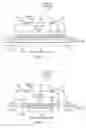
FIG. 1 is a cross sectional depiction of an example electronic assembly, according to an example embodiment.
FIG. 2 is a cross sectional depiction of another example electronic assembly, according to an example embodiment.
FIGS. 3A-C show top view depictions after successive steps in an example assembly method using a disclosed substrate to form the electronic assembly shown in FIG. 1, according to an example embodiment.
DETAILED DESCRIPTION
Example embodiments are described with reference to the drawings, wherein like reference numerals are used to designate similar or equivalent elements. Illustrated ordering of acts or events should not be considered as limiting, as some acts or events may occur in different order and/or concurrently with other acts or events. Furthermore, some illustrated acts or events may not be required to implement a methodology in accordance with this disclosure.
FIG. 1 is a cross sectional depiction of an example electronic assembly 100 before encapsulation, according to an example embodiment. Electronic assembly 100 is shown comprising a substrate 110 that includes a die pad 105. The die pad 105 includes an outer raised flat portion 115 and a recessed portion that includes an inner recessed portion 120. A semiconductor die 125 is directly on the outer raised flat portion 115 and is affixed to the die pad by a die attach material 130 that is on the inner recessed portion 120. The die attach material 130 can be seen to not be on a top surface 116 of the outer raised flat portion 115.
Substrate 110 in the embodiment shown in FIG. 1 includes a metal layer 111 that is on a dielectric material 112, such as a polyimide in one particular embodiment. The outer raised flat portion 115 of substrate 110 can be provided by a dielectric material, such as in the form of a solder resist layer. The dielectric material, such in the form of a patterned solder resist layer, is shown providing the outer raised flat portion 115 that defines the inner recessed portion 120, which also exposes the plurality bond pads 111(a) and 111(b).
Solder resist (or solder mask) as used herein and known in the art is a lacquer-like layer of polymer (e.g., an epoxy) that provides a permanent protective coating for metal (e.g., copper) traces of substrates including printed circuit boards (PCBs) that prevents solder from bridging between conductors, thereby preventing short circuits. One solder resist material is epoxy liquid that is silkscreened through a pattern onto the substrate. Other types are the liquid photoimageable solder mask (LPSM) inks and dry film photoimageable solder mask (DFSM). All three of these processes go through a thermal cure of some type after the pattern is defined.
Metal layer 111 provides metal traces a plurality of substrate contact pad regions, such as contact pad regions 111(a) and 111(b) that are shown coupled to bond pads 126 on semiconductor die 125 by bond wires 132. FIG. 1 shows a gap 139 under the semiconductor die 125 along at least a portion of a boundary between an outer edge of said die attach material 130 on the interior recessed portion 120 and an inside edge of the raised flat portion 115. The gap 139 shown demonstrates that there is no need for complete (100%) filling of the inner recessed portion 120 with the die attach material 130, which can save cost by conserving die attach material.
FIG. 2 is a cross sectional depiction of another example electronic assembly 200 before encapsulation, according to an example embodiment. The substrate 210 comprises a metal or metal alloy (that may include a thin surface metal layer) that is part of a lead frame that includes a plurality of lead fingers 211(a) and 211(b) positioned outside at least one side of the die pad 205. The outer raised flat portion 115 of die pad 205 in this embodiment also comprises the metal or metal alloy provide by substrate 210. Bond pads 132 on the semiconductor die 125 are connected by bond wires 132 to the plurality of lead fingers 211(a), 211(b).
FIGS. 3A-C show top view depictions after some of the successive steps in an example assembly method using a disclosed substrate to form the electronic assembly 100 shown in FIG. 1, according to an example embodiment. Although a single electronic assembly is described as being formed, it is understood that typically a large number of electronic assemblies will be simultaneously formed, and a substrate panel (e.g., organic polymer panel) or substrate sheet (e.g., lead frame sheet) will provide a plurality of interconnected substrates for simultaneous assembly. The depiction 310 shown in FIG. 3A is after forming a patterned solder resist layer on a dielectric material 112 that includes an outer raised flat portion 115 that defines an inner recessed portion 120, where the inner recessed portion 120 further comprises a plurality of slits 311 that are exclusive of solder resist material. The slits 311 are connected to the inner recessed portion 120. Metal traces are shown as 111(c) providing coupling to the die pad 120 and contact pad regions 111(a) and 111(b).
The depiction 340 shown in FIG. 3B is after dispensing of die attach material (e.g., paste) to the area of the inner recessed portion 120, that can generally by accomplished by standard die attach dispense equipment. The depiction 370 shown in FIG. 3C is after die attachment of semiconductor die 125 (with the semiconductor die 125 depicted as optically transparent to show the die attach material 130) onto the die pad 105 where the die attach material 130 can be seen to have flown along the slits 311. Following wirebonding to add bond wires shown in FIG. 1 as 132, the electronic assembly shown in FIG. 1A is formed. An encapsulation step generally follows wirebonding, followed by singulation.
Disclosed substrates can also be used for a variety of electronic assemblies. One example is for flip chip mounted semiconductor die.
Advantages of disclosed embodiments include the ability to use industry standard equipment. Moreover, there is no need for 100% coverage of the die attach material, thus saving die attach material. Other advantages include the ability to mount with larger die sizes without increasing die pad size, or the package footprint.
Disclosed embodiments can be integrated into a variety of assembly flows to form a variety of different IC devices and related products. Those skilled in the art to which this disclosure relates will appreciate that many other embodiments and variations of embodiments are possible within the scope of the claimed invention, and further additions, deletions, substitutions and modifications may be made to the described embodiments without departing from the scope of this disclosure.
Claims
1. An electronic assembly, comprising:
a substrate including a die pad, wherein said die pad includes and an outer raised flat portion and a recessed portion that includes an inner recessed portion, and
a semiconductor die directly on said outer raised flat portion and affixed to said die pad by a die attach material in said inner recessed portion, wherein said die attach material is not on a top surface of said outer raised flat portion.
2. The electronic assembly of claim 1, wherein said substrate comprises a metal or metal alloy and is part of a lead frame that includes a plurality of lead fingers positioned outside at least one side of said die pad, and wherein bond pads on said semiconductor die are connected to said plurality of lead fingers.
3. The electronic assembly of claim 1, wherein said substrate comprises a dielectric substrate having a top substrate surface and a metal or metal alloy layer on said top substrate surface including a plurality substrate bond pads that are positioned outside at least one side of said die pad,
further comprising a solder resist layer comprising a solder resist material on said metal layer, wherein said solder resist material inside said die pad provides said outer raised flat portion, defines said recessed portion, and exposes said plurality bond pads, wherein said semiconductor die has its bottomside affixed to said die pad.
4. The electronic assembly of claim 3, wherein said inner recessed portion is exclusive of said solder resist material.
5. The electronic assembly of claim 4, wherein said recessed portion further comprises at least one slit that is exclusive of said solder resist, and wherein said slit is connected to said inner recessed portion, and said die attach material is also within said slit.
6. The electronic assembly of claim 5, wherein said at least one slit comprises a plurality of said slits.
7. The electronic assembly of claim 1, wherein a gap exists under said semiconductor die along at least a portion of a boundary between an outer edge of said die attach material on said inner recessed portion and an inside edge of said outer raised flat portion.
8. An electronic assembly, comprising:
a dielectric substrate having a top substrate surface;
a metal layer on said top substrate surface including a plurality bond pads that are positioned outside at least one side of a die pad region;
a solder resist layer comprising a solder resist material on said metal layer, wherein said solder resist material inside said die pad provides an outer raised flat portion, defines an inner recessed portion, and exposes said plurality bond pads,
a die attach adhesive on said inner recessed portion but not on a top surface of said outer raised portion, and
a semiconductor die having its bottomside attached to said die pad region, wherein an outer portion of said bottomside is directly on said top surface of said outer raised portion and an inner portion of said bottomside is affixed to said die attach adhesive.
9. The electronic assembly of claim 8, wherein said inner recessed portion is exclusive of said solder resist material.
10. The electronic assembly of claim 8, wherein said recessed portion further comprises at least one slit that is exclusive of said solder resist, wherein said slit is connected to said inner recessed portion, and wherein said die attach material is also within said slit.
11. A method of forming an electronic assembly, comprising:
dispensing a die attach material on a substrate into a recessed portion that includes an inner recessed portion of a die pad of said substrate that includes an outer raised flat portion, but not on said outer raised flat portion, and
attaching a semiconductor die directly on said outer raised flat portion and affixing said semiconductor die with said die attach material in said interior recessed portion but not on said outer raised flat portion.
12. The method of claim 11, wherein said substrate comprises a metal or metal alloy and is part of a lead frame that includes a plurality of lead fingers that are outside at least one side of said die pad, and wherein bond pads on said semiconductor die are connected to said plurality of lead fingers.
13. The method of claim 11, wherein said substrate comprises a dielectric substrate having a top substrate surface and a metal or metal alloy layer on said top substrate surface including a plurality substrate bond pads that are positioned outside at least one side of said die pad,
further comprising a solder resist layer comprising a solder resist material on said metal layer, wherein said solder resist layer inside said die pad provides said outer raised flat portion, defines said inner recessed portion, and exposes said plurality bond pads, wherein said semiconductor die has its bottomside affixed to said die pad by said die attach material.
14. The method of claim 11, wherein said inner recessed portion is exclusive of said solder resist material.
15. The method of claim 13, wherein said recessed portion further comprises at least one slit that is exclusive of said solder resist, and wherein said slit is connected to said inner recessed portion, and said die attach material is also within said slit after said attaching.
16. The method of claim 15, wherein said at least one slit comprises a plurality of said slits.
17. The method of claim 11, wherein a gap exists under said semiconductor die along at least a portion of a boundary between an outer edge of said die attach material on said inner recessed portion and an inside edge of said outer raised flat portion.
Images & Drawings included:


Sources:
- United States Patent and Trademark Office - verify current appl. status at the USPTO↗
Similar patent applications:
Recent applications in this class:
- » 20250293200 2025-09-18
LAMINATE MANUFACTURING METHOD, INSULATION MATERIAL, AND LAMINATE - » 20250286015 2025-09-11
PIEZOELECTRIC MATERIALS FOR ON-DIE THERMAL ENHANCEMENT OF HYBRID BONDING AND ASSOCIATED SYSTEMS AND METHODS - » 20250279392 2025-09-04
METHOD FOR PRODUCING SEMICONDUCTOR DEVICE, AND SEMICONDUCTOR DEVICE - » 20250279391 2025-09-04
SEMICONDUCTOR PACKAGE - » 20250279390 2025-09-04
METHOD FOR MANUFACTURING SEMICONDUCTOR PACKAGE DEVICE - » 20250279389 2025-09-04
BONDING TOOL FOR BONDING DIES ONTO SUBSTRATES AND METHODS OF USE - » 20250273621 2025-08-28
SUBSTRATE PROCESSING METHOD, PLASMA PROCESSING APPARATUS, AND SUBSTRATE PROCESSING SYSTEM - » 20250273620 2025-08-28
METHOD FOR DIE-TO-DIE HYBRID BONDING USING AN ADVANCED DISTRIBUTION MODEL - » 20250273619 2025-08-28
METHOD OF HYBRID BONDING USING DIE DISTRIBUTION MODEL - » 20250246575 2025-07-31
Apparatus and Bonding Process for Wafer Bonding
Recent applications for this Assignee:
- » 20250291595 2025-09-18
CIRCUIT, SYSTEM, AND METHOD FOR MATRIX DECIMATION - » 20250286550 2025-09-11
TRANSISTOR SHUTDOWN CIRCUT - » 20250279725 2025-09-04
CONDUCTION MODE CONTROL - » 20250274138 2025-08-28
SWITCH REGULATOR - » 20250267687 2025-08-21
ENHANCED BROADCAST TRANSMISSION IN UNSLOTTED CHANNEL HOPPING MEDIUM ACCESS CONTROL - » 20250266825 2025-08-21
BOOTSTRAP CIRCUIT - » 20250247097 2025-07-31
LEVEL SHIFTER CIRCUIT - » 20250247082 2025-07-31
LOW AREA AND POWER MULTI-BIT FLIP-FLOP - » 20250246995 2025-07-31
SWITCHING CONVERTER DEADTIME CONTROL - » 20250246345 2025-07-31
TRIMMING RESISTOR USING MODULATED SIGNAL