Serial advanced technology attachment dual in-line memory module
US20130128446A1
2013-05-23
13/316,492
2011-12-10
✅ Patent granted
US 8,514,603 B2
2013-08-20
-
-
Fernando Hidalgo
Altis Law Group, Inc.
2031-12-10
Abstract:
A serial advanced technology attachment dual in-line memory module (SATA DIMM) includes a control chip having a first input output (I/O) pin and a second I/O pin, first and second switches, a resistor, and a number of storage chips connected to the control chip. First terminals of the first and second switches are respectively connected to the first and second I/O pins. Second terminals of the first and second switches are grounded. The first and second I/O pins receive different signals through controlling the first and second switches, to change work modes of the storage chips.
Inventors:
- GUO-YI CHEN 43 🇨🇳 Shenzhen City, China
- XIAO-GANG YIN 14 🇨🇳 Shenzhen City, China
- GUO-YI CHEN 71 🇨🇳 Shenzhen, China
- Xiao-Gang Yin 38 🇨🇳 Shenzhen, China
Assignee:
- HON HAI PRECISION INDUSTRY CO., LTD. 12,833 🇹🇼 Tu-Cheng, Taiwan
- HONG FU JIN PRECISION INDUSTRY (SHENZHEN) CO., LTD. 4,225 🇨🇳 Shenzhen City, China
- HON HAI PRECISION INDUSTRY CO., LTD. 10,014 🇹🇼 New Taipei, Taiwan
- HONG FU JIN PRECISION INDUSTRY (ShenZhen) CO., LTD. 2,585 🇨🇳 Shenzhen, China
Applicant:
Interested in similar patents?
Get notified when new applications in this technology area are published.
Classification:
G06F13/4234 » CPC main
Interconnection of, or transfer of information or other signals between, memories, input/output devices or central processing units; Information transfer, e.g. on bus; Bus transfer protocol, e.g. handshake; Synchronisation on a parallel bus being a memory bus
G06F3/0607 » CPC further
Input arrangements for transferring data to be processed into a form capable of being handled by the computer; Output arrangements for transferring data from processing unit to output unit, e.g. interface arrangements; Digital input from, or digital output to, record carriers, e.g. RAID, emulated record carriers or networked record carriers; Interfaces specially adapted for storage systems specifically adapted to achieve a particular effect; Improving or facilitating administration, e.g. storage management by facilitating the process of upgrading existing storage systems, e.g. for improving compatibility between host and storage device
G06F3/0634 » CPC further
Input arrangements for transferring data to be processed into a form capable of being handled by the computer; Output arrangements for transferring data from processing unit to output unit, e.g. interface arrangements; Digital input from, or digital output to, record carriers, e.g. RAID, emulated record carriers or networked record carriers; Interfaces specially adapted for storage systems making use of a particular technique; Configuration or reconfiguration of storage systems by changing the state or mode of one or more devices
G06F3/0679 » CPC further
Input arrangements for transferring data to be processed into a form capable of being handled by the computer; Output arrangements for transferring data from processing unit to output unit, e.g. interface arrangements; Digital input from, or digital output to, record carriers, e.g. RAID, emulated record carriers or networked record carriers; Interfaces specially adapted for storage systems adopting a particular infrastructure; In-line storage system; Single storage device Non-volatile semiconductor memory device, e.g. flash memory, one time programmable memory [OTP]
G11C5/04 » CPC further
Details of stores covered by group; Disposition of storage elements, e.g. in the form of a matrix array Supports for storage elements, e.g. memory modules ; Mounting or fixing of storage elements on such supports
G06F2213/0032 » CPC further
Indexing scheme relating to interconnection of, or transfer of information or other signals between, memories, input/output devices or central processing units Serial ATA [SATA]
G06F1/16 IPC
Details not covered by groups - and Constructional details or arrangements
G11C5/06 IPC
Details of stores covered by group Arrangements for interconnecting storage elements electrically, e.g. by wiring
Description
BACKGROUND
1. Technical Field
The present disclosure relates to solid state drives (SSD), and particularly to a serial advanced technology attachment dual in-line memory module (SATA DIMM).
2. Description of Related Art
Solid state drives (SSD) store data on chips instead of on magnetic or optical discs. One type of SSD has the form factor of a DIMM module and it is called a SATA DIMM module. The SATA DIMM module includes a plurality of storage chips and can be inserted into a memory slot of a motherboard, to add storage capacity. However, different types of storage chips have different work modes. Thus, layout of the SATA DIMM module needs to be changed when the storage chip needs to be replaced, causing inconvenience.
BRIEF DESCRIPTION OF THE DRAWING
Many aspects of the embodiments can be better understood with parameter to the following drawing. The components in the drawing are not necessarily drawn to scale, the emphasis instead being placed upon clearly illustrating the principles of the present embodiments. Moreover, in the drawing, like numerals designate corresponding parts throughout the several views.
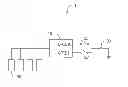
The FIGURE is a circuit diagram of a serial advanced technology attachment dual in-line memory module in accordance with an exemplary embodiment of the present disclosure.
DETAILED DESCRIPTION
The disclosure, including the drawing, is illustrated by way of example and not by way of limitation. References to “an” or “one” embodiment in this disclosure are not necessarily to the same embodiment, and such references mean at least one.
Referring to the FIGURE, a serial advanced technology attachment dual in-line memory module (SATA DIMM) 1 can be inserted into a memory slot, such as a double data rate three type (DDR3) memory slot of a computer (not shown), to add storage capacity. The SATA DIMM module 1 in accordance with an exemplary embodiment includes a control chip 10, switches S1 and S2, a resistor 30, and a plurality of storage chips 40 connected to the control chip 10.
A first terminal of the switch S1 is connected to an input output (I/O) pin general purpose input output (GPIO) 10 of the control chip 10. A first terminal of the switch S2 is connected to an I/O pin GPIO11 of the control chip 10. Second terminals of the switches S1 and S2 are grounded through the resistor 30.
The I/O pins GPIO10 and GPIO11 of the control chip 10 receive different signals according to the states of the switches Si and S2, and control the work modes of the storage chips 40 according to the received level signals. For example, when the I/O pins GPIO10 and GPIO11 receive low level signals, the storage chips 40 work in a first work mode, such as an Async mode. When the I/O pin GPIO10 is at a high level state and the I/O pin GPIO11 receives a low level signal, the storage chips 40 work in a second work mode, such as a Toggle mode. When the I/O pin GPIO10 receives a low level signal and the I/O pin GPIO11 is at a high level state, the storage chips 40 work in a third work mode, such as an ONFI2 mode. When the I/O pins GPIO10 and GPIO11 are both at high level states, the storage chips 40 work in a fourth work mode, such as an Old async mode.
In use, when the storage chips 40 need to work in the first work mode, the switches S1 and S2 are both closed, the I/O pins GPIO10 and GPIO11 of the control chip 10 receive low level signals. The control chip 10 controls the storage chips 40 to work in the first work mode. When the storage chips 40 need to work in the second work mode, the switch S1 is opened, and the switch S2 is closed. The I/O pin GPIO10 is at a high level state and the I/O pin GPIO11 receives a low level signal. The control chip 10 controls the storage chips 40 to work in the second work mode. When the storage chips 40 need to work in the third work mode, the switch S1 is closed and the switch S2 is opened. The I/O pin GPIO10 receives a low level signal and the I/O pin GPIO11 is at a high level state. The control chip 10 controls the storage chips 40 to work in the third work mode. When the storage chips 40 need to work in the fourth work mode, the switches Si and S2 are opened. The I/O pins GPIO10 and GPIO11 are both at high level states. The control chip 10 controls the storage chips 40 to work in the fourth work mode.
The SATA DIMM module 1 can change the work modes of the storage chips 40 through the switches S1 and S2, which is convenient.
Even though numerous characteristics and advantages of the disclosure have been set forth in the foregoing description, together with details of the structure and function of the disclosure, the disclosure is illustrative only, and changes may be made in detail, especially in the matters of shape, size, and arrangement of parts within the principles of the disclosure to the full extent indicated by the broad general meaning of the terms in which the appended claims are expressed.
Claims
What is claimed is:1. A serial advanced technology attachment dual in-line memory module (SATA DIMM) comprising:
a control chip comprising a first input output (I/O) pin and a second I/O pin;
a resistor;
a first switch comprising a first terminal and a second terminal, wherein the first terminal is connected to the first I/O pin of the control chip, the second terminal is grounded;
a second switch comprising a first terminal and a second terminal, wherein the first terminal of the second switch is connected to the second I/O pin of the control chip, the second terminal of the second switch is grounded; and
a plurality of storage chips connected to the control chip;
wherein the first and second I/O pins of the control chip receive different signals through controlling the first and second switches, to change work modes of the plurality of storage chips.
2. The SATA DIMM module of claim 1, wherein the work modes of the storage chips comprises first to fourth work modes, the first work mode is an Async mode, the second work mode is a Toggle mode, the third work mode is an ONFI2 mode, the fourth work mode is an Old async mode; when the first and second I/O pins receive low level signals through closing the first and second switches, the storage chips work in the first work mode; when the first I/O pin is at a high level state and the second I/O pin receives a low level signal through opening the first switch but closing the second switch, the storage chips work in the second work mode; when the first I/O pin receives a low level signal and the second I/O pin is at a high level state through closing the first switch but opening the second switch, the storage chips work in the third work mode; when the first and second I/O pins are at high level states through opening the first and second switches, the storage chips work in the fourth work mode.
3. The SATA DIMM module of claim 1, wherein the second terminals of the first and second switches are grounded through a resistor.
Images & Drawings included:

Sources:
- United States Patent and Trademark Office - verify current appl. status at the USPTO↗
Similar patent applications:
- » 20130016471
Serial advanced technology attachment dual in-line memory module device assembly - » 20130038997
Motherboard assembly having serial advanced technology attachment dual in-line memory module - » 20130038999
Expansion apparatus for serial advanced technology attachment dual in-line memory module and motherboard for supporting the expansion apparatus - » 20130039016
Motherboard assembly having serial advanced technology attachment dual in-line memory module - » 20130044424
Motherboard for supporting expansion card or serial advanced technology attachment dual in-line memory module through same expansion slot - » 20130044450
Motherboard assembly having serial advanced technology attachment dual in-line memory module - » 20130050970
Motherboard assembly having serial advanced technology attachment dual in-line memory module - » 20130070410
SERIAL ADVANCED TECHNOLOGY ATTACHMENT DUAL IN-LINE MEMORY MODULE AND COMPUTER SYSTEM - » 20130070411
Serial advanced technology attachment dual in-line memory module assembly - » 13564762
Serial advanced technology attachment dual in-line memory module (SATA DIMM) capable of preventing data loss
Recent applications for this Assignee:
- » 20250218287 2025-07-03
METHOD OF GENERATING AND PROMPTING TRAFFIC INFORMATION, AND ROADSIDE DEVICE THEREOF - » 20250178535 2025-06-05
METHOD FOR CONSTRUCTING 3D PANORAMIC VIEW MODEL, VEHICLE-MOUNTED DEVICE, AND STORAGE MEDIUM - » 20250074444 2025-03-06
METHOD FOR EARLY WARNING A BLIND AREA, ELECTRONIC DEVICE AND STORAGE MEDIUM - » 20240416754 2024-12-19
DISPLAY CONTROL DEVICE, DISPLAY EQUIPMENT, AND VEHICLE EMPLOYING DEVICE - » 20240411051 2024-12-12
Light-emitting device array and optical transceiver system having the same - » 20240324114 2024-09-26
DISPLAY CONTROL DEVICE AND VEHICLE EMPLOYING DEVICE - » 20240295957 2024-09-05
METHOD FOR CONTROLLING ELECTRONIC DEVICE, ELECTRONIC DEVICE AND COMPUTER STROAGE MEDIUM EMPLOYING METHOD - » 20240257357 2024-08-01
METHOD FOR DETECTING OBSTACLES, ELECTRONIC DEVICE, AND STORAGE MEDIUM - » 20240203133 2024-06-20
LANE LINE RECOGNITION METHOD, ELECTRONIC DEVICE AND STORAGE MEDIUM - » 20240194999 2024-06-13
Robot using limiting device for locking battery