Carrier, semiconductor package and fabrication method thereof
US20130187285A1
2013-07-25
13/440,180
2012-04-05
✅ Patent granted
US 8,680,692 B2
2014-03-25
-
-
David Zarneke
Edwards Wildman Palmer LLP | Peter F. Corless | Steven M. Jensen
2032-04-18
Abstract:
A fabrication method of a semiconductor package includes the steps of: providing a carrier having a concave portion and a releasing layer formed on a surface thereof; disposing a chip on the releasing layer in the concave portion; forming an encapsulant on the chip and the releasing layer; removing the releasing layer and the carrier; and forming a circuit structure on the encapsulant and the chip. The design of the concave portion facilitates alignment of the chip to prevent it from displacement, thereby improving the product reliability. A semiconductor package fabricated by the fabrication method is also provided.
Inventors:
- Shih-Kuang Chiu 42 🇹🇼 Taichung, Taiwan
- Chiang-Cheng Chang 19 🇹🇼 Taichung, Taiwan
- Meng-Tsung Lee 15 🇹🇼 Taichung, Taiwan
- Jung-Pang Huang 14 🇹🇼 Taichung, Taiwan
Assignee:
- Siliconware Precision Industries Co., Ltd. 673 🇹🇼 Taichung, Taiwan
Applicant:
Interested in similar patents?
Get notified when new applications in this technology area are published.
Classification:
H01L21/561 » CPC further
Processes or apparatus adapted for the manufacture or treatment of semiconductor or solid state devices or of parts thereof; Manufacture or treatment of semiconductor devices or of parts thereof the devices having at least one potential-jump barrier or surface barrier, e.g. PN junction, depletion layer or carrier concentration layer; Assembly of semiconductor devices using processes or apparatus not provided for in a single one of the subgroups - , e.g. sealing of a cap to a base of a container; Encapsulations, e.g. encapsulation layers, coatings Batch processing
H01L21/568 » CPC further
Processes or apparatus adapted for the manufacture or treatment of semiconductor or solid state devices or of parts thereof; Manufacture or treatment of semiconductor devices or of parts thereof the devices having at least one potential-jump barrier or surface barrier, e.g. PN junction, depletion layer or carrier concentration layer; Assembly of semiconductor devices using processes or apparatus not provided for in a single one of the subgroups - , e.g. sealing of a cap to a base of a container; Encapsulations, e.g. encapsulation layers, coatings Temporary substrate used as encapsulation process aid
H01L21/673 » CPC further
Processes or apparatus adapted for the manufacture or treatment of semiconductor or solid state devices or of parts thereof; Apparatus specially adapted for handling semiconductor or electric solid state devices during manufacture or treatment thereof; Apparatus specially adapted for handling wafers during manufacture or treatment of semiconductor or electric solid state devices or components ; Apparatus not specifically provided for elsewhere using specially adapted carriers or holders; Fixing the workpieces on such carriers or holders
H01L21/76877 » CPC further
Processes or apparatus adapted for the manufacture or treatment of semiconductor or solid state devices or of parts thereof; Manufacture or treatment of devices consisting of a plurality of solid state components formed in or on a common substrate or of parts thereof; Manufacture of integrated circuit devices or of parts thereof; Manufacture of specific parts of devices defined in group; Applying interconnections to be used for carrying current between separate components within a device comprising conductors and dielectrics characterised by the formation and the after-treatment of the conductors Filling of holes, grooves or trenches, e.g. vias, with conductive material
H01L21/78 » CPC further
Processes or apparatus adapted for the manufacture or treatment of semiconductor or solid state devices or of parts thereof; Manufacture or treatment of devices consisting of a plurality of solid state components formed in or on a common substrate or of parts thereof; Manufacture of integrated circuit devices or of parts thereof; Manufacture or treatment of devices consisting of a plurality of solid state components or integrated circuits formed in, or on, a common substrate with subsequent division of the substrate into plural individual devices
H01L23/3114 » CPC further
Details of semiconductor or other solid state devices; Encapsulations, e.g. encapsulating layers, coatings, e.g. for protection characterised by the arrangement or shape the device being completely enclosed the device being a chip scale package, e.g. CSP
H01L24/19 » CPC further
Arrangements for connecting or disconnecting semiconductor or solid-state bodies; Methods or apparatus related thereto; Means for bonding being attached to, or being formed on, the surface to be connected, e.g. chip-to-package, die-attach, "first-level" interconnects; Manufacturing methods related thereto; High density interconnect [HDI] connectors; Manufacturing methods related thereto Manufacturing methods of high density interconnect preforms
H01L24/96 » CPC further
Arrangements for connecting or disconnecting semiconductor or solid-state bodies; Methods or apparatus related thereto; Batch processes at chip-level, i.e. with connecting carried out on a plurality of singulated devices, i.e. on diced chips the devices being encapsulated in a common layer, e.g. neo-wafer or pseudo-wafer, said common layer being separable into individual assemblies after connecting
H01L21/566 » CPC further
Processes or apparatus adapted for the manufacture or treatment of semiconductor or solid state devices or of parts thereof; Manufacture or treatment of semiconductor devices or of parts thereof the devices having at least one potential-jump barrier or surface barrier, e.g. PN junction, depletion layer or carrier concentration layer; Assembly of semiconductor devices using processes or apparatus not provided for in a single one of the subgroups - , e.g. sealing of a cap to a base of a container; Encapsulations, e.g. encapsulation layers, coatings; Moulds Release layers for moulds, e.g. release layers, layers against residue during moulding
H01L21/67333 » CPC further
Processes or apparatus adapted for the manufacture or treatment of semiconductor or solid state devices or of parts thereof; Apparatus specially adapted for handling semiconductor or electric solid state devices during manufacture or treatment thereof; Apparatus specially adapted for handling wafers during manufacture or treatment of semiconductor or electric solid state devices or components ; Apparatus not specifically provided for elsewhere using specially adapted carriers or holders; Fixing the workpieces on such carriers or holders Trays for chips
H01L21/67763 » CPC further
Processes or apparatus adapted for the manufacture or treatment of semiconductor or solid state devices or of parts thereof; Apparatus specially adapted for handling semiconductor or electric solid state devices during manufacture or treatment thereof; Apparatus specially adapted for handling wafers during manufacture or treatment of semiconductor or electric solid state devices or components ; Apparatus not specifically provided for elsewhere for conveying, e.g. between different workstations the wafers being stored in a carrier, involving loading and unloading
H01L21/68 » CPC further
Processes or apparatus adapted for the manufacture or treatment of semiconductor or solid state devices or of parts thereof; Apparatus specially adapted for handling semiconductor or electric solid state devices during manufacture or treatment thereof; Apparatus specially adapted for handling wafers during manufacture or treatment of semiconductor or electric solid state devices or components ; Apparatus not specifically provided for elsewhere for positioning, orientation or alignment
H01L21/683 » CPC further
Processes or apparatus adapted for the manufacture or treatment of semiconductor or solid state devices or of parts thereof; Apparatus specially adapted for handling semiconductor or electric solid state devices during manufacture or treatment thereof; Apparatus specially adapted for handling wafers during manufacture or treatment of semiconductor or electric solid state devices or components ; Apparatus not specifically provided for elsewhere for supporting or gripping
H01L23/31 » CPC further
Details of semiconductor or other solid state devices; Encapsulations, e.g. encapsulating layers, coatings, e.g. for protection characterised by the arrangement or shape
H01L23/3107 » CPC further
Details of semiconductor or other solid state devices; Encapsulations, e.g. encapsulating layers, coatings, e.g. for protection characterised by the arrangement or shape the device being completely enclosed
H01L23/3121 » CPC further
Details of semiconductor or other solid state devices; Encapsulations, e.g. encapsulating layers, coatings, e.g. for protection characterised by the arrangement or shape the device being completely enclosed a substrate forming part of the encapsulation
H01L24/05 » CPC further
Arrangements for connecting or disconnecting semiconductor or solid-state bodies; Methods or apparatus related thereto; Means for bonding being attached to, or being formed on, the surface to be connected, e.g. chip-to-package, die-attach, "first-level" interconnects; Manufacturing methods related thereto; Bonding areas ; Manufacturing methods related thereto; Structure, shape, material or disposition of the bonding areas prior to the connecting process of an individual bonding area
H01L24/13 » CPC further
Arrangements for connecting or disconnecting semiconductor or solid-state bodies; Methods or apparatus related thereto; Means for bonding being attached to, or being formed on, the surface to be connected, e.g. chip-to-package, die-attach, "first-level" interconnects; Manufacturing methods related thereto; Bump connectors ; Manufacturing methods related thereto; Structure, shape, material or disposition of the bump connectors prior to the connecting process of an individual bump connector
H01L2224/02379 » CPC further
Indexing scheme for arrangements for connecting or disconnecting semiconductor or solid-state bodies and methods related thereto as covered by; Means for bonding being attached to, or being formed on, the surface to be connected, e.g. chip-to-package, die-attach, "first-level" interconnects; Manufacturing methods related thereto; Bonding areas; Manufacturing methods related thereto; Redistribution layers [RDL] for bonding areas; Disposition of the redistribution layers Fan-out arrangement
H01L2224/0401 » CPC further
Indexing scheme for arrangements for connecting or disconnecting semiconductor or solid-state bodies and methods related thereto as covered by; Means for bonding being attached to, or being formed on, the surface to be connected, e.g. chip-to-package, die-attach, "first-level" interconnects; Manufacturing methods related thereto; Bonding areas; Manufacturing methods related thereto; Structure, shape, material or disposition of the bonding areas prior to the connecting process Bonding areas specifically adapted for bump connectors, e.g. under bump metallisation [UBM]
H01L2224/04105 » CPC further
Indexing scheme for arrangements for connecting or disconnecting semiconductor or solid-state bodies and methods related thereto as covered by; Means for bonding being attached to, or being formed on, the surface to be connected, e.g. chip-to-package, die-attach, "first-level" interconnects; Manufacturing methods related thereto; Bonding areas; Manufacturing methods related thereto; Structure, shape, material or disposition of the bonding areas prior to the connecting process Bonding areas formed on an encapsulation of the semiconductor or solid-state body, e.g. bonding areas on chip-scale packages
H01L2224/12105 » CPC further
Indexing scheme for arrangements for connecting or disconnecting semiconductor or solid-state bodies and methods related thereto as covered by; Means for bonding being attached to, or being formed on, the surface to be connected, e.g. chip-to-package, die-attach, "first-level" interconnects; Manufacturing methods related thereto; Bump connectors; Manufacturing methods related thereto; Structure, shape, material or disposition of the bump connectors prior to the connecting process Bump connectors formed on an encapsulation of the semiconductor or solid-state body, e.g. bumps on chip-scale packages
H01L2224/97 » CPC further
Indexing scheme for arrangements for connecting or disconnecting semiconductor or solid-state bodies and methods related thereto as covered by; Batch processes at chip-level, i.e. with connecting carried out on a plurality of singulated devices, i.e. on diced chips the devices being connected to a common substrate, e.g. interposer, said common substrate being separable into individual assemblies after connecting
H01L2924/1815 » CPC further
Indexing scheme for arrangements or methods for connecting or disconnecting semiconductor or solid-state bodies as covered by; Details of package parts other than the semiconductor or other solid state devices to be connected; Encapsulation Shape
H01L2224/11 » CPC further
Indexing scheme for arrangements for connecting or disconnecting semiconductor or solid-state bodies and methods related thereto as covered by; Means for bonding being attached to, or being formed on, the surface to be connected, e.g. chip-to-package, die-attach, "first-level" interconnects; Manufacturing methods related thereto; Bump connectors; Manufacturing methods related thereto Manufacturing methods
H01L2224/96 » CPC further
Indexing scheme for arrangements for connecting or disconnecting semiconductor or solid-state bodies and methods related thereto as covered by; Batch processes at chip-level, i.e. with connecting carried out on a plurality of singulated devices, i.e. on diced chips the devices being encapsulated in a common layer, e.g. neo-wafer or pseudo-wafer, said common layer being separable into individual assemblies after connecting
H01L2224/03 » CPC further
Indexing scheme for arrangements for connecting or disconnecting semiconductor or solid-state bodies and methods related thereto as covered by; Means for bonding being attached to, or being formed on, the surface to be connected, e.g. chip-to-package, die-attach, "first-level" interconnects; Manufacturing methods related thereto; Bonding areas; Manufacturing methods related thereto Manufacturing methods
H01L2924/014 » CPC further
Indexing scheme for arrangements or methods for connecting or disconnecting semiconductor or solid-state bodies as covered by; Alloys Solder alloys
H01L23/48 IPC
Details of semiconductor or other solid state devices Arrangements for conducting electric current to or from the solid state body in operation, e.g. leads, terminal arrangements ; Selection of materials therefor
H01L21/50 IPC
Processes or apparatus adapted for the manufacture or treatment of semiconductor or solid state devices or of parts thereof; Manufacture or treatment of semiconductor devices or of parts thereof the devices having at least one potential-jump barrier or surface barrier, e.g. PN junction, depletion layer or carrier concentration layer Assembly of semiconductor devices using processes or apparatus not provided for in a single one of the subgroups - , e.g. sealing of a cap to a base of a container
H01L21/56 » CPC main
Processes or apparatus adapted for the manufacture or treatment of semiconductor or solid state devices or of parts thereof; Manufacture or treatment of semiconductor devices or of parts thereof the devices having at least one potential-jump barrier or surface barrier, e.g. PN junction, depletion layer or carrier concentration layer; Assembly of semiconductor devices using processes or apparatus not provided for in a single one of the subgroups - , e.g. sealing of a cap to a base of a container Encapsulations, e.g. encapsulation layers, coatings
H01L23/28 IPC
Details of semiconductor or other solid state devices Encapsulations, e.g. encapsulating layers, coatings, e.g. for protection
Description
BACKGROUND OF THE INVENTION
1. Field of the Invention
The present invention relates to semiconductor packages and fabrication methods thereof, and more particularly, to a semiconductor package having an embedded chip and a fabrication method thereof.
2. Description of Related Art
Along with the rapid development of electronic industries, electronic products are developed towards multi-function and high performance. To meet the miniaturization requirement of semiconductor packages, wafer level packaging (WLP) technologies have been developed.
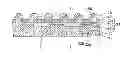
U.S. Pat. No. 6,452,265 and No. 7,202,107 provide fabrication methods of wafer-level packages. FIGS. 1A to 1E are cross-sectional views showing a fabrication method of a semiconductor package 1 according to the prior art.
Referring to FIG. 1A, a thermal adhesive layer 11 is formed on a carrier 10.
Referring to FIG. 1B, a plurality of chips 12 are disposed on the thermal adhesive layer 11. Each of the chips 12 has an active surface 12a with a plurality of electrode pads 120 and an inactive surface 12b opposite to the active surface 12a, and the chips 12 are disposed on the thermal adhesive layer 11 via the active surfaces 12a thereof.
Referring to FIG. 1C, an encapsulant 13 is formed on the chips 12 and the thermal adhesive layer 11.
Referring to FIG. 1D, the thermal adhesive layer 11 and the carrier 10 are removed to expose the active surfaces 12a of the chips 12.
Referring to FIG. 1E, a circuit structure 14 is formed on the encapsulant 13 and the active surfaces 12a of the chips 12 and electrically connected to the electrode pads 120 of the chips 12.
However, when the chips 12 are disposed on the plate-shaped carrier 10 having the thermal adhesive layer 11, it is difficult to align the chips 12 on the carrier, thus easily causing displacement of the chips 12 and reducing the product reliability.
In addition, since the thermal adhesive layer 11 is adhesive, it may expand or contract due to its coefficient of thermal expansion (CTE) during the fabrication process, such that displacement of the chips 12 tends to occur. For example, during formation of the encapsulant 13, the thermal adhesive layer 11 is softened by heat to cause displacement of the chips 12. Consequently, the circuit structure 14 to be formed later cannot be precisely connected to the electrode pads 120 of the chips 12, thereby resulting in poor electrical performance and product reliability.
Therefore, how to overcome the above-described drawbacks has become critical.
SUMMARY OF THE INVENTION
In view of the above-described drawbacks, the present invention provides a semiconductor package, which comprises: an encapsulant having a protruding portion; a chip embedded in the protruding portion of the encapsulant, wherein the chip has an active surface with a plurality of electrode pads and an inactive surface opposite to the active surface, the active surface and the electrode pads being exposed from the protruding portion of the encapsulant; and a circuit structure formed on the encapsulant and the active surface of the chip and electrically connected to the electrode pads of the chip.
The present invention further provides a fabrication method of a semiconductor package, which comprises the steps of: providing a carrier having a concave portion and a releasing layer formed on a surface thereof; disposing a chip on the releasing layer in the concave portion, wherein the chip has an active surface with a plurality of electrode pads and an inactive surface opposite to the active surface, the chip being disposed on the releasing layer via the active surface thereof; forming an encapsulant on the chip and the releasing layer; removing the releasing layer and the carrier so as to expose the active surface of the chip; and forming a circuit structure on the encapsulant and the active surface of the chip, wherein the circuit structure is electrically connected to the electrode pads of the chip.
The present invention further provides a carrier for fabricating a semiconductor package, wherein the carrier has a concave portion and a releasing layer formed on a surface thereof.
In an embodiment, the carrier can be made of glass or metal, and the releasing layer can be made of a hydrophobic material, an inorganic material or a polymer material.
In an embodiment, a plurality of concave portions are provided and array arranged on the carrier such that the above-described method further comprises performing a singulation process after forming the circuit structure on the encapsulant and the active surface of the chip.
In an embodiment, the carrier is removed first and then the releasing layer is removed. Alternatively, the carrier and the releasing layer can be removed simultaneously.
In an embodiment, the circuit structure has at least a dielectric layer formed on the encapsulant and the active surface of the chip, a circuit layer formed on the dielectric layer and a plurality of conductive vias formed in the dielectric layer for electrically connecting the circuit layer and the electrode pads of the chip. Further, an insulating protection layer can be formed on the outermost dielectric layer of the circuit structure and have a plurality of openings therein such that portions of the circuit layer are exposed through the openings so as for conductive elements to be disposed thereon.
Therefore, through the design of the concave portion on the carrier, the present invention facilitates alignment of the chip so as to prevent it from displacement that may otherwise impose difficulty in subsequent fabrication processes such as a circuit built-up process and reduce the product reliability.
Further, since the releasing layer is not adhesive, the releasing layer does not expand or contract due to its CTE during the fabrication process, thereby avoiding displacement of the chip, facilitating subsequent fabrication processes and improving the product reliability.
BRIEF DESCRIPTION OF DRAWINGS
FIGS. 1A to 1E are schematic cross-sectional views showing a fabrication method of a semiconductor package according to the prior art; and
FIGS. 2A to 2G are schematic cross-sectional views showing a fabrication method of a semiconductor package according to the present invention, wherein FIG. 2A′ is an upper view of FIG. 2A and FIG. 2E′ shows another embodiment of FIG. 2E.
DETAILED DESCRIPTION OF PREFERRED EMBODIMENTS
The following illustrative embodiments are provided to illustrate the disclosure of the present invention, these and other advantages and effects can be apparent to those in the art after reading this specification.
It should be noted that the drawings are only for illustrative purposes and not intended to limit the present invention. Meanwhile, terms such as ‘on’, ‘a’ etc. are only used as a matter of descriptive convenience and not intended to have any other significance or provide limitations for the present invention.
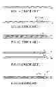
FIGS. 2A to 2G are schematic cross-sectional views showing a fabrication method of a semiconductor package 2 according to the present invention.
Referring to FIGS. 2A and 2A′, a carrier 20 having a plurality of concave portions 200 is provided. In the present embodiment, the carrier 20 is made of glass or metal, and the concave portions 200 are array arranged on the carrier 20.
Referring to FIG. 2B, a releasing layer 21 is formed on the carrier 20 and the concave portions 200.
In the present embodiment, the releasing layer 21 is made of a hydrophobic material, an inorganic material or a polymer material such as poly-para-xylylene (parylene), and formed through plasma-enhanced chemical vapor deposition (PECVD).
The present invention replaces the conventional thermal adhesive material with the releasing layer 21 to reduce the fabrication cost.
Referring to FIG. 2C, a plurality of chips 22 are disposed on the releasing layer 21 in the concave portions 200, respectively. Each of the chips 22 has an active surface 22a with a plurality of electrode pads 220 and an inactive surface 22b opposite to the active surface 22a, and the chips 22 are disposed on the releasing layer 21 via the active surfaces 22a thereof.
The concave portions 200 facilitate alignment of the chips 22 so as to avoid displacement of the chips 22.
Further, since the releasing layer 21 is not adhesive, particularly to the carrier 20 made of glass, the releasing layer 21 does not expand or extract due to its CTE during the fabrication process, thereby avoiding displacement of the chips 22. As such, a circuit structure to be formed in a subsequent circuit built-up process can be effectively and precisely electrically connected to the electrode pads 220 of the chips 22 such that the electrical performance and product reliability can be improved.
Referring to FIG. 2D, an encapsulant 23 is formed on the chips 22 and the releasing layer 21.
In the present embodiment, the encapsulant 23 is made of, but not limited to, polyimide (PI), and formed through coating. Alternatively, the encapsulant 23 can be formed through lamination or molding.
Referring to FIG. 2E, the releasing layer 21 and the carrier 20 are removed to expose the active surfaces 22a of the chips 22 and a plurality of protruding portions 230 of the encapsulant 23.
In the present embodiment, the carrier 20 is first removed from the releasing layer 21 and then the releasing layer 21 is removed from the encapsulant 23 and the chip 22.
In another embodiment, the releasing layer 21 can be removed from the encapsulant 23 and the chips 22 simultaneously with the carrier 20, as shown in FIG. 2E′.
Referring to FIG. 2F, a circuit built-up process is performed to form a circuit structure 24 on the encapsulant 23 and the active surfaces 22a of the chips 22. Therein, the circuit structure 24 is electrically connected to the electrode pads 220 of the chips 22.
In the present embodiment, the circuit structure 24 has at least a dielectric layer 240, a circuit layer 241 formed on the dielectric layer 240 and a plurality of conductive vias 242 formed in the dielectric layer 230 for electrically connecting the circuit layer 241 and the electrode pads 220 of the chips 22. Therein, the number of the dielectric layers 240 can be multiple, and the number of the circuit layer 241 can be increased to meet circuit layout requirements of the semiconductor package.
Subsequently, an insulating protection layer 25 is formed on the outermost dielectric layer 240 and a plurality of openings 250 are formed in the insulating protection layer 25 such that portions of the circuit layer 241 are exposed through the openings 250 so as for conductive elements 26 to be disposed thereon. The conductive elements 26 can be, but not limited to, solder balls, solder bumps or solder pins.
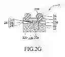
Referring to FIG. 2G a singulation process is performed along cutting lines L of FIG. 2F so as to obtain a plurality of semiconductor packages 2.
The present invention further provides a semiconductor package 2, which has: an encapsulant 23 having a protruding portion 230; a chip 22 embedded in the protruding portion 230; and a circuit structure 24 formed on the encapsulant 23.
The chip 22 has an active surface 22a with a plurality of electrode pads 220 and an inactive surface 22b opposite to the active surface 22a, and the active surface 22a and the electrode pads 220 are exposed from the protruding portion 230 of the encapsulant 23.
The circuit structure 24 is formed on the active surface 22a of the chip 22 and electrically connected to the electrode pads 220 of the chip 22. The circuit structure 24 has at least a dielectric layer 240, a circuit layer 241 formed on the dielectric layer 240 and a plurality of conductive vias 242 formed in the dielectric layer 240 for electrically connecting the circuit layer 241 and the electrode pads 220 of the chip 22.
Furthermore, an insulating protection layer 25 is formed on the outermost dielectric layer 240 of the circuit structure 24 and has a plurality of openings 250 formed therein such that portions of the circuit layer 241 are exposed through the openings 250 so as for conductive elements 26 to be disposed thereon.
Therefore, through the design of the concave portions on the carrier, the present invention facilitates alignment of the chips so as to avoid displacement of the chips, thereby improving the product reliability.
Also, since the releasing layer is not adhesive, it will not cause displacement of the chips. Therefore, the product reliability is further improved.
The above-described descriptions of the detailed embodiments are only to illustrate the preferred implementation according to the present invention, and it is not to limit the scope of the present invention. Accordingly, all modifications and variations completed by those with ordinary skill in the art should fall within the scope of present invention defined by the appended claims.
Claims
What is claimed is:1. A semiconductor package, comprising:
an encapsulant having a protruding portion;
a chip embedded in the protruding portion of the encapsulant, wherein the chip has an active surface with a plurality of electrode pads and an inactive surface opposite to the active surface, the active surface and the electrode pads being exposed from the protruding portion of the encapsulant; and
a circuit structure formed on the encapsulant and the active surface of the chip and electrically connected to the electrode pads of the chip.
2. The package of claim 1, wherein the circuit structure has at least a dielectric layer formed on the encapsulant and the active surface of the chip, a circuit layer formed on the dielectric layer, and a plurality of conductive vias formed in the dielectric layer for electrically connecting the circuit layer and the electrode pads of the chip.
3. The package of claim 2, further comprising an insulating protection layer formed on the outermost dielectric layer of the circuit structure and having a plurality of openings formed therein such that portions of the circuit layer are exposed through the openings so as for conductive elements to be disposed thereon.
4. A fabrication method of a semiconductor package, comprising the steps of:
providing a carrier having a concave portion and a releasing layer formed on a surface thereof;
disposing a chip on the releasing layer in the concave portion, wherein the chip has an active surface with a plurality of electrode pads and an inactive surface opposite to the active surface, the chip being disposed on the releasing layer via the active surface thereof;
forming an encapsulant on the chip and the releasing layer;
removing the releasing layer and the carrier so as to expose the active surface of the chip; and
forming a circuit structure on the encapsulant and the active surface of the chip, wherein the circuit structure is electrically connected to the electrode pads of the chip.
5. The method of claim 4, wherein the carrier is made of glass or metal.
6. The method of claim 4, wherein a plurality of concave portions are provided and array arranged on the carrier.
7. The method of claim 6, after forming the circuit structure on the encapsulant and the active surface of the chip, further comprising performing a singulation process.
8. The method of claim 4, wherein the releasing layer is made of a hydrophobic material, an inorganic material or a polymer material.
9. The method of claim 4, wherein the carrier is removed first and then the releasing layer is removed.
10. The method of claim 4, wherein the releasing layer and the carrier are removed simultaneously.
11. The method of claim 4, wherein the circuit structure has at least a dielectric layer formed on the encapsulant and the active surface of the chip, a circuit layer formed on the dielectric layer and a plurality of conductive vias formed in the dielectric layer for electrically connecting the circuit layer and the electrode pads of the chip.
12. The method of claim 11, further comprising forming an insulating protection layer on the outermost dielectric layer of the circuit structure and forming a plurality of openings in the insulating protection layer such that portions of the circuit layer are exposed through the openings so as for conductive elements to be disposed thereon.
13. A carrier for fabricating a semiconductor package, having a concave portion and a releasing layer disposed on a surface thereof.
14. The carrier of claim 13, wherein the carrier is made of glass or metal.
15. The carrier of claim 13, wherein the releasing layer is made of a hydrophobic material, an inorganic material or a polymer material.
Images & Drawings included:
Sources:
- United States Patent and Trademark Office - verify current appl. status at the USPTO↗
Similar patent applications:
- » 20140154842
Carrier, semiconductor package and fabrication method thereof - » 20130009311
SEMICONDUCTOR CARRIER, PACKAGE AND FABRICATION METHOD THEREOF - » 20060121647
Carrier-free semiconductor package and fabrication method thereof - » 20160079110
SEMICONDUCTOR PACKAGE, CARRIER STRUCTURE AND FABRICATION METHOD THEREOF - » 20150325508
Semiconductor package and fabrication method thereof and carrier structure - » 20060060958
Semiconductor package, and fabrication method and carrier thereof - » 20070018291
Semiconductor package without chip carrier and fabrication method thereof - » 20120007234
Semiconductor package without chip carrier and fabrication method thereof - » 20070273019
Semiconductor package, chip carrier structure thereof, and method for fabricating the chip carrier - » 10196305
Flip-chip semiconductor package with lead frame as chip carrier and fabrication method thereof
Recent applications in this class:
- » 20130334697 2013-12-19
Integrated circuit packaging system with through silicon via and method of manufacture thereof - » 20130329373 2013-12-12
Bio-implantable hermetic integrated ultra high density device - » 20130320530 2013-12-05
Semiconductor device with redistributed contacts - » 20130319620 2013-12-05
BOARD SEPARATION APPARATUS AND OPERATING METHOD THEREOF - » 20130260511 2013-10-03
Lid attach process and apparatus for fabrication of semiconductor packages - » 20130187260 2013-07-25
Packaged semiconductor devices including pre-molded lead-frame structures, and related methods and systems - » 20130175687 2013-07-11
Package stack device and fabrication method thereof - » 20130168849 2013-07-04
Fully molded fan-out - » 20130168848 2013-07-04
Packaged semiconductor device with a molding compound and a method of forming the same - » 20130168805 2013-07-04
Packages with passive devices and methods of forming the same
Recent applications for this Assignee:
- » 20250046771 2025-02-06
METHOD FOR FABRICATING ELECTRONIC PACKAGE - » 20250015054 2025-01-09
CARRYING SUBSTRATE, ELECTRONIC PACKAGE HAVING THE CARRYING SUBSTRATE, AND METHODS FOR MANUFACTURING THE SAME - » 20240379534 2024-11-14
ELECTRONIC PACKAGE, MANUFACTURING METHOD FOR THE SAME, AND ELECTRONIC STRUCTURE - » 20240321798 2024-09-26
Electronic package and carrier thereof and method for manufacturing the same - » 20240321784 2024-09-26
Electronic package including lead frame having multiple conductive posts - » 20240321591 2024-09-26
METHOD FOR FABRICATING ELECTRONIC PACKAGE - » 20240290701 2024-08-29
ELECTRONIC PACKAGE AND MANUFACTURING METHOD THEREOF - » 20240290675 2024-08-29
Electronic package and manufacturing method thereof - » 20240290674 2024-08-29
ELECTRONIC PACKAGE AND MANUFACTURING METHOD THEREOF - » 20240282674 2024-08-22
ELECTRONIC PACKAGE AND METHOD OF FABRICATING THE SAME