SEMICONDUCTOR PACKAGE STRUCTURE
US20130341807A1
2013-12-26
13/531,601
2012-06-25
Abstract:
A semiconductor package structure includes a package substrate having a first surface, a second surface opposite to the first surface, and a sidewall surface between the first surface and the second surface. A semiconductor device is mounted on the first surface. A mold cap encapsulates the semiconductor device. The mold cap includes a vertical extension portion covering the sidewall surface and a horizontal extension portion covering a periphery of a solder ball implanting region on the second surface.
Interested in similar patents?
Get notified when new applications in this technology area are published.
Classification:
H01L2924/181 » CPC further
Indexing scheme for arrangements or methods for connecting or disconnecting semiconductor or solid-state bodies as covered by; Details of package parts other than the semiconductor or other solid state devices to be connected Encapsulation
H01L2924/00012 » CPC further
Indexing scheme for arrangements or methods for connecting or disconnecting semiconductor or solid-state bodies as covered by; Technical content checked by a classifier Relevant to the scope of the group, the symbol of which is combined with the symbol of this group
H01L23/28 IPC
Details of semiconductor or other solid state devices Encapsulations, e.g. encapsulating layers, coatings, e.g. for protection
H01L23/3128 » CPC main
Details of semiconductor or other solid state devices; Encapsulations, e.g. encapsulating layers, coatings, e.g. for protection characterised by the arrangement or shape the device being completely enclosed a substrate forming part of the encapsulation the substrate having spherical bumps for external connection
H01L23/13 » CPC further
Details of semiconductor or other solid state devices; Mountings, e.g. non-detachable insulating substrates characterised by the shape
H01L23/49816 » CPC further
Details of semiconductor or other solid state devices; Arrangements for conducting electric current to or from the solid state body in operation, e.g. leads, terminal arrangements ; Selection of materials therefor consisting of soldered constructions; Leads, on insulating substrates,; Additional leads joined to the metallisation on the insulating substrate, e.g. pins, bumps, wires, flat leads Spherical bumps on the substrate for external connection, e.g. ball grid arrays [BGA]
H01L2224/73265 » CPC further
Indexing scheme for arrangements for connecting or disconnecting semiconductor or solid-state bodies and methods related thereto as covered by; Means for bonding being of different types provided for in two or more of groups; Location after the connecting process on different surfaces Layer and wire connectors
H01L2924/1815 » CPC further
Indexing scheme for arrangements or methods for connecting or disconnecting semiconductor or solid-state bodies as covered by; Details of package parts other than the semiconductor or other solid state devices to be connected; Encapsulation Shape
H01L2924/00014 » CPC further
Indexing scheme for arrangements or methods for connecting or disconnecting semiconductor or solid-state bodies as covered by; Technical content checked by a classifier the subject-matter covered by the group, the symbol of which is combined with the symbol of this group, being disclosed without further technical details
H01L2924/15311 » CPC further
Indexing scheme for arrangements or methods for connecting or disconnecting semiconductor or solid-state bodies as covered by; Details of package parts other than the semiconductor or other solid state devices to be connected; Die mounting substrate; Connection portion the connection portion being formed only on the surface of the substrate opposite to the die mounting surface being a ball array, e.g. BGA
H01L2224/73215 » CPC further
Indexing scheme for arrangements for connecting or disconnecting semiconductor or solid-state bodies and methods related thereto as covered by; Means for bonding being of different types provided for in two or more of groups; Location after the connecting process on the same surface Layer and wire connectors
H01L2924/00 » CPC further
Indexing scheme for arrangements or methods for connecting or disconnecting semiconductor or solid-state bodies as covered by
Description
BACKGROUND OF THE INVENTION
1. Field of the Invention
The present invention relates to a package structure, particularly to a semiconductor package structure capable of reducing warpage and preventing delamination.
2. Description of the Prior Art
As known in the art, semiconductor integrated circuits are fabricated on a semiconductor wafer by using a number of process steps, for example, film deposition, ion implantation, etching and lithographic processes. After wafer fabrication, the wafer is subjected to die singulation process that is typically performed by using a saw blade. The individual die is then packaged together with a package substrate or chip carrier. Typically, during a packaging process, the chip or die is encapsulated by molded polymer resin that also partially encapsulating a top surface of the package substrate on which the die is mounted.
One problem with the molded plastic package is that subsequent to molding, internal delamination frequently occurs. In severe cases, a crack develops, creating an ingress site for contaminants resulting in reliability issue of the chip package. The location that is particularly prone to delamination is the interface of the package substrate and the molding resin. Delamination at the interface of the package substrate and the molding resin is primarily due to inadequate adhesion between the substrate and the molding resin and/or stresses generated by coefficient of thermal expansion mismatch and singularizing process. Another problem with the molded plastic package is the package warpage induced by thermal stress and package structure unbalance.
SUMMARY OF THE INVENTION
It is one object of the invention to provide an improved semiconductor package structure to overcome the above-mentioned prior art problems and shortcomings.
According to one aspect of the present invention, a semiconductor package structure includes a package substrate having a first surface, a second surface opposite to the first surface, and a sidewall surface between the first surface and the second surface; a semiconductor device mounted on the first surface; a plurality of bond wires electrically coupling the semiconductor device to the package substrate; and a mold cap encapsulating at least the semiconductor device and the bond wires, wherein the mold cap comprises a vertical extension portion covering the entire sidewall surface and a horizontal extension portion covering a periphery of a solder ball implanting region on the second surface.
These and other objectives of the present invention will no doubt become obvious to those of ordinary skill in the art after reading the following detailed description of the preferred embodiment that is illustrated in the various figures and drawings.
BRIEF DESCRIPTION OF THE DRAWINGS
FIG. 1 is a schematic, cross-sectional diagram showing a semiconductor package structure capable of reducing warpage and preventing delamination in accordance with one embodiment of this invention.
FIG. 2 is a schematic, cross-sectional diagram showing a semiconductor package structure capable of reducing warpage and preventing delamination in accordance with another embodiment of this invention.
DETAILED DESCRIPTION
In the following detailed description, reference is made to the accompanying drawings, which form a part hereof, and in which is shown by way of illustration specific examples in which the embodiments may be practiced. These embodiments are described in sufficient detail to enable those skilled in the art to practice them, and it is to be understood that other embodiments may be utilized and that structural, logical and electrical changes may be made without departing from the described embodiments. The following detailed description is, therefore, not to be taken in a limiting sense, and the included embodiments are defined by the appended claims.
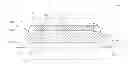
FIG. 1 is a schematic, cross-sectional diagram showing a semiconductor package structure capable of reducing warpage and preventing delamination in accordance with one embodiment of this invention. As shown in FIG. 1, the semiconductor package structure la comprises a package substrate 10 having a first surface 10a, a second surface 10c that is opposite to the first surface 10a, and a sidewall surface 10b between the first surface 10a and the second surface 10c. The sidewall surface 10b is substantially perpendicular to both of the first surface 10a and the second surface 10c. The package substrate 10 may be a plastic substrate having an insulating core layer such as glass-fiber materials or the like, and multiple layers of conductive traces and multiple layers of dielectric materials laminated on the insulating core layer. The multiple layers of conductive traces may be interconnected to each other by using a plurality of via plugs or so-called plated through holes (PTHs). Optionally, a solder mask (not explicitly shown) may be used to cover either the first surface 10a or the second surface 10c to protect the topmost layer of the conductive traces. It is to be understood that the package substrate may be ant other type of substrate such as molding compound or epoxy based substrate wherein the solder mask may be omitted.
A semiconductor device 20 such as a semiconductor integrated circuit chip is mounted on the first surface 10a within a predetermined chip-mounting region. The semiconductor device 20 may be adhered to the first surface 10a by using an adhesive layer 22. The semiconductor device 20 has an active surface 20a having thereon a plurality of bonding pads 202. The bonding pads 202 are electrically connected to respective bond fingers 112 disposed on the first surface 10a of the package substrate 10 with a plurality of bond wires 32. In an alternative case, the semiconductor device 20 may be flipped and with it active surface face-down mounted on the first surface 10a via bumps or the like. On the second surface 10c of the package substrate 10, a solder ball implanting region 200 is defined. A plurality of solder pads 114 are provided on the second surface 10c within the solder ball implanting region 200. A plurality of solder balls 40 are formed on respective solder pads 114.
A mold cap 30 is provided to encapsulate the semiconductor device 20, the bond wires 32, and at least a portion of the top surface 10a of the package substrate 10. The mold cap 30 further extends to the second surface 10c to cover a periphery of the solder ball implanting region 200. In another embodiment, the aforesaid adhesive layer 22 may be replaced with the mold cap 30. As shown in FIG. 1, the mold cap 30 comprises a vertical extension portion 30a that covers the entire sidewall surface 10b and a horizontal extension portion 30b that may act as a mold lock to resist package warpage. The vertical extension portion 30a connects the main portion of the mold cap 30 to the underlying horizontal extension portion 30b. Since the entire sidewall surface 10b is covered with the horizontal extension portion 30b, delamination can be prevented.
FIG. 2 is a schematic, cross-sectional diagram showing a semiconductor package structure capable of reducing warpage and preventing delamination in accordance with another embodiment of this invention, wherein like numeral numbers designate like regions, layers or elements. As shown in FIG. 2, the semiconductor package structure lb comprises a package substrate 10 having a central slot or window 102. A semiconductor device 20 such as a DDR DRAM chip is provided face-down mounted on the first surface 10a of the package substrate 10. The active surface 20a of the semiconductor device 20 is electrically coupled to the second surface 10c through the bond wires 32 that pass through the window 102. Likewise, a mold cap 30 is provided to encapsulate the semiconductor device 20, the bond wires 32, the window 102, and at least a portion of the top surface 10a of the package substrate 10. The mold cap 30 further extends to the second surface 10c to cover a periphery of the solder ball implanting region 200. The mold cap 30 comprises a vertical extension portion 30a that covers the entire sidewall surface 10b and a horizontal extension portion 30b that may act as a mold lock to resist package warpage. The vertical extension portion 30a connects the main portion of the mold cap 30 to the underlying horizontal extension portion 30b. Since the entire sidewall surface 10b is covered with the horizontal extension portion 30b, delamination can be prevented.
Those skilled in the art will readily observe that numerous modifications and alterations of the device and method may be made while retaining the teachings of the invention. Accordingly, the above disclosure should be construed as limited only by the metes and bounds of the appended claims.
Claims
What is claimed is:1. A semiconductor package structure, comprising:
a package substrate having a first surface, a second surface opposite to the first surface, and a sidewall surface between the first surface and the second surface;
a semiconductor device mounted on the first surface; and
a mold cap encapsulating at least the semiconductor device, wherein the mold cap comprises a vertical extension portion covering the sidewall surface and a horizontal extension portion covering a periphery of a solder ball implanting region on the second surface.
2. The semiconductor package structure according to claim 1 wherein the vertical extension portion connects a main portion of the mold cap to the horizontal extension portion.
3. The semiconductor package structure according to claim 1 wherein the package substrate comprises a slot.
4. The semiconductor package structure according to claim 3 further comprising a plurality of bond wires electrically coupling the semiconductor device to the package substrate.
5. The semiconductor package structure according to claim 4 wherein the bond wires pass through the slot.
6. The semiconductor package structure according to claim 1 further comprising an adhesive layer to adhere the semiconductor device to the first surface of the package substrate.
7. The semiconductor package structure according to claim 1 further comprising a solder mask covering either the first surface or the second surface.
Images & Drawings included:

Sources:
- United States Patent and Trademark Office - verify current appl. status at the USPTO↗
Similar patent applications:
- » 20220301989
Substrate structure, semiconductor package structure and method for manufacturing semiconductor package structure - » 20190181108
Semiconductor Package Structure and Semiconductor Package Structure Fabricating Method - » 20250132266
METHOD OF MANUFACTURING SEMICONDUCTOR PACKAGE STRUCTURE AND SEMICONDUCTOR PACKAGE STRUCTURE - » 20250149347
METHOD FOR FABRICATING SEMICONDUCTOR PACKAGING STRUCTURE AND SEMICONDUCTOR PACKAGING STRUCTURE FABRICATED USING THE SAME - » 20110079890
Semiconductor package, semiconductor package structure including the semiconductor package, and mobile phone including the semiconductor package structure - » 20110233755
Semiconductor housing package, semiconductor package structure including the semiconductor housing package, and processor-based system including the semiconductor package structure - » 20210143119
Semiconductor package structures, semiconductor device packages and methods of manufacturing the same - » 20180174954
Wiring structure, semiconductor package structure and semiconductor process - » 20230062138
Semiconductor package structure and method for forming semiconductor package structure - » 20240055408
SEMICONDUCTOR PACKAGE STRUCTURE AND METHOD FOR PREPARING SEMICONDUCTOR PACKAGE STRUCTURE
Recent applications in this class:
- » 20130320548 2013-12-05
Integrated circuit die assembly with heat spreader - » 20130270717 2013-10-17
Semiconductor package including chip support and method of fabricating the same - » 20130249073 2013-09-26
INTEGRATED CIRCUIT PACKAGING SYSTEM WITH SUPPORT STRUCTURE AND METHOD OF MANUFACTURE THEREOF - » 20130241053 2013-09-19
Integrated circuit packaging system with conductive pillars and molded cavities and method of manufacture thereof - » 20130228915 2013-09-05
SEMICONDUCTOR PACKAGE AND FABRICATION METHOD THEREOF - » 20130224914 2013-08-29
Method for package-on-package assembly with wire bonds to encapsulation surface - » 20130221543 2013-08-29
Integrated circuit packaging system with interconnects - » 20130193575 2013-08-01
OPTIMIZATION OF COPPER PLATING THROUGH WAFER VIA - » 20130157418 2013-06-20
Integrated circuit packaging system with interconnects and method of manufacture thereof - » 20130154105 2013-06-20
Integrated circuit packaging system with routable trace and method of manufacture thereof