Image sensor module and camera module using same
US20140055669A1
2014-02-27
13/726,653
2012-12-26
✅ Patent granted
US 9,007,499 B2
2015-04-14
-
-
Yogesh Aggarwal
Novak Druce Connolly Bove + Quigg LLP
2033-02-16
Abstract:
An image sensor module includes a ceramic substrate, an image sensor, a conductive film, and a bottom plate. The ceramic substrate includes an upper surface, a lower surface opposite to the upper surface, a side surface connected between the upper surface and the lower surface. The ceramic substrate has a through hole through the upper and lower surfaces, a receiving recess on the lower surface, and an air hole on the side surface. The through hole communicates with the receiving recess, and the air hole communicates with the receiving recess. The image sensor is received in the receiving recess and is electrically connected to the ceramic substrate. The bottom plate is positioned on the lower surface and electrically connected to the ceramic substrate by the conductive film.
Assignee:
- HON HAI PRECISION INDUSTRY CO., LTD. 10,014 🇹🇼 New Taipei, Taiwan
Applicant:
Interested in similar patents?
Get notified when new applications in this technology area are published.
Classification:
H01L27/14618 » CPC main
Devices consisting of a plurality of semiconductor or other solid-state components formed in or on a common substrate including semiconductor components sensitive to infra-red radiation, light, electromagnetic radiation of shorter wavelength or corpuscular radiation and specially adapted either for the conversion of the energy of such radiation into electrical energy or for the control of electrical energy by such radiation; Devices controlled by radiation; Imager structures; Structural or functional details thereof Containers
H04N5/2253 » CPC further
Details of television systems; Studio circuitry; Studio devices; Studio equipment ; Cameras comprising an electronic image sensor, e.g. digital cameras, video cameras, TV cameras, video cameras, camcorders, webcams, camera modules for embedding in other devices, e.g. mobile phones, computers or vehicles; Television cameras ; Cameras comprising an electronic image sensor, e.g. digital cameras, video cameras, camcorders, webcams, camera modules specially adapted for being embedded in other devices, e.g. mobile phones, computers or vehicles; Constructional details Mounting of pick-up device, electronic image sensor, deviation or focusing coils
H04N5/2254 » CPC further
Details of television systems; Studio circuitry; Studio devices; Studio equipment ; Cameras comprising an electronic image sensor, e.g. digital cameras, video cameras, TV cameras, video cameras, camcorders, webcams, camera modules for embedding in other devices, e.g. mobile phones, computers or vehicles; Television cameras ; Cameras comprising an electronic image sensor, e.g. digital cameras, video cameras, camcorders, webcams, camera modules specially adapted for being embedded in other devices, e.g. mobile phones, computers or vehicles; Constructional details Mounting of optical parts, e.g. lenses, shutters, filters or optical parts peculiar to the presence or use of an electronic image sensor
H04N3/14 IPC
Scanning details of television systems; Combination thereof with generation of supply voltages by means not exclusively optical-mechanical by means of electrically scanned solid-state devices
H04N5/335 IPC
Details of television systems; Transforming light or analogous information into electric information using solid-state image sensors [SSIS]
H01L27/146 IPC
Devices consisting of a plurality of semiconductor or other solid-state components formed in or on a common substrate including semiconductor components sensitive to infra-red radiation, light, electromagnetic radiation of shorter wavelength or corpuscular radiation and specially adapted either for the conversion of the energy of such radiation into electrical energy or for the control of electrical energy by such radiation; Devices controlled by radiation Imager structures
H04N5/225 IPC
Details of television systems; Studio circuitry; Studio devices; Studio equipment ; Cameras comprising an electronic image sensor, e.g. digital cameras, video cameras, TV cameras, video cameras, camcorders, webcams, camera modules for embedding in other devices, e.g. mobile phones, computers or vehicles Television cameras ; Cameras comprising an electronic image sensor, e.g. digital cameras, video cameras, camcorders, webcams, camera modules specially adapted for being embedded in other devices, e.g. mobile phones, computers or vehicles
Description
BACKGROUND
1. Technical Field
The present disclosure relates to optical modules, and particularly, to an image sensor module and a camera module including the image sensor module.
2. Description of Related Art
Image sensor modules generally include a ceramic substrate, an image sensor, and a circuit board module. The image sensor is electrically connected on a lower surface of the ceramic substrate by a method of flip-chip package. The ceramic substrate is positioned on the circuit board module and electrically connected to the circuit board module by conductive glue. The image sensor is received between the circuit board module and the ceramic substrate. However, in testing, the image sensor module is subjected to heating and the conductive glue will generate gas. As such, the air pressure between the ceramic substrate and the circuit board module will increase and the ceramic substrate may be forced away from the circuit board module, resulting in a bad electrical connection.
Therefore, it is desirable to provide an image sensor module and a camera module, which can overcome the limitations described.
BRIEF DESCRIPTION OF THE DRAWINGS
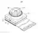
FIG. 1 is an isometric view of a camera module in accordance with an exemplary embodiment.
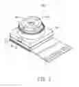
FIG. 2 is an isometric, exploded, and schematic view of the camera module of FIG. 1.
FIG. 3 is similar to FIG. 1, but viewed from another angle.
FIG. 4 is a cross-sectional view taken along a line IV-IV of FIG. 1.
DETAILED DESCRIPTION
Embodiments of the disclosure will be described with reference to the drawings.
FIGS. 1-3 show a camera module 100 according to an exemplary embodiment. The camera module 100 includes an image sensor module 200 and a lens module 300 positioned on the image sensor module 200. The image sensor module 200 includes a bottom plate 10, a conductive film 20, a ceramic substrate 30, an image sensor 40, a filling body 50, and a filter 60. The lens module 300 includes a lens holder 70, and a lens unit 80.
The bottom plate 10 is rectangular and is an electrical circuit board. The bottom plate 10 includes a flexible printed circuit board (FPCB) 11, an adhesive layer 12, and a stiffening plate 13. The adhesive layer 12 is adhered between the FPCB 11 and the stiffening plate 13. The FPCB 11 includes a first surface 111 and a second surface 112 opposite to the first surface 111. A number of connecting pads 113 are formed on the first surface 111, generally adjacent to opposite edges of the FPCB 11. The stiffening plate 13 adheres to the second surface 112 of the FPCB 11. The mechanical strength of the FPCB 11 is effectively increased by adding the stiffening plate 13.
The conductive film 20 is an anisotropic conductive film, and is adhered on the first surface 111 of the FPCB 11. The conductive film 20 is electrically connected to the FPCB 11 along a direction perpendicular to the first surface 111 and is electrically disconnected to the FPCB 11 along a direction parallel with the first surface 111 when the conductive film 20 is subjected to a hot pressing process.
The ceramic substrate 30 includes an upper surface 31, a lower surface 32 opposite to the upper surface 31, and a side surface 33 connecting the upper surface 31 and the lower surface 32. The ceramic substrate 30 defines a through hole 311 through the upper surface 31 and the lower surface 32, a receiving recess 321 on the lower surface 32, and an air hole 331 on the side surface 33. The through hole 311 communicates with the receiving recess 321. The air hole 321 also communicates with the receiving recess 321, and passes all the way through the lower surface 32. The receiving recess 321 includes a connecting surface 322 parallel to the upper surface 31. A number of first pads 323 are formed on the connecting surface 322, and a number of second pads 324 are formed on the lower surface 32. The first pads 323 are connected to the second pads 324 by wires buried in the ceramic substrate 30.
The image sensor 40 includes an image surface 41 and a number of pins 42 adjacent to opposite edges of the image surface 41. The image sensor 40 converts light rays striking the image surface 41 into image signals in form of electric signals, and the image signals are output from the pins 42. In the embodiment, the image sensor 40 can be a complementary metal-oxide-semiconductor transistor (CMOS) sensor or a charge coupled device (CCD) sensor.
The filling body 50 functions as a frame, and is made of an opaque glue. The opaque glue is applied into to a mold and then is cured.
The filter 60 is rectangular, and is transparent, made of a material, such as glass. The filter 60 filters out infrared light from the light passing through.
FIG. 4 shows an assembling process of the image sensor module 200. The image sensor 20 is received in the receiving recess 321, and the image surface 41 faces the through hole 311. The pins 42 are electrically connected to the first pads 323. The filling body 50 is received in the receiving recess 321, and surrounds the image sensor 40. In the embodiment, the opaque glue is applied into the receiving recess 321 and surrounds the image sensor 40, and then the opaque glue is cured. The lower surface 32 of the ceramic substrate 30 is supported on the first surface 111 of the FPCB 11, the second pads 324 are electrically connected to the connecting pads 113 by the conductive film 20. The filter 60 is positioned on the upper surface 31 of the ceramic substrate 30, and the through hole 311 is covered by the filter 60.
The lens holder 70 includes a seat 71 and a receiving portion 72 positioned on one end of the seat 71. The seat 71 is hollow shaped. The receiving portion 72 defines a receiving hole 721 communicating with the seat 71. The lens unit 80 is received in the receiving hole 721, and includes at least one lens (not shown) and a barrel receiving the at least one lens.
In the process of assembling the camera module 100, the lens holder 70 receiving the lens unit 80 is positioned on the upper surface 31 of the ceramic substrate 30. The seat 61 surrounds the through hole 311. The filter 60 is received in the seat 71. The optical axis of the lens unit 80 coincides with the optical axis of the image sensor 40.
In use, the image sensor 40 converts the light rays penetrating the lens module 300 into image signals. The image signals are output to the FPCB 11 through the pins 42, the first pads 323, the second pads 324, and the connecting pads 113. As the stiffening plate 13 is added on the FPCB 11, the mechanical strength of the FPCB 11 and the conductive film 20 are effectively increased, and the conductive film 20 will not block or seal the air hole 331 of the ceramic substrate 30.
Particular embodiments are shown and described by way of illustration only. The principles and the features of the present disclosure may be employed in various and numerous embodiments thereof without departing from the scope of the disclosure as claimed. The above-described embodiments illustrate the scope of the disclosure but do not restrict the scope of the disclosure.
Claims
What is claimed is:1. An image sensor module, comprising:
a ceramic substrate comprising an upper surface, a lower surface opposite to the upper surface, a side surface connected between the upper surface and the lower surface; the ceramic substrate defining a through hole through the upper and lower surfaces, a receiving recess on the lower surface, and an air hole on the side surface; the through hole communicating with the receiving recess, the air hole communicating with the receiving recess;
an image sensor received in the receiving recess and electrically connected to the ceramic substrate;
a conductive film; and
a bottom plate positioned on the lower surface of the ceramic substrate and electrically connected to the ceramic substrate by the conductive film.
2. The image sensor module of claim 1, wherein the bottom plate comprises a flexible printed circuit board (FPCB), an adhesive layer, and a stiffening plate; the adhesive layer is adhered between the FPCB and the stiffening plate.
3. The image sensor module of claim 1, wherein the receiving recess comprises a connecting surface parallel with the upper surface, a plurality of first pads positioned on the connecting surface, and a plurality of second pads positioned on the lower surface; the first pads are correspondingly connected to the second pads.
4. The image sensor module of claim 3, wherein the image sensor comprises an image surface and a plurality of pins adjacent to the image surface, the pins are electrically connected to the first pads.
5. The image sensor module of claim 1, wherein the air hole passes all the way through the lower surface.
6. A camera module, comprising:
an image sensor module, comprising:
a ceramic substrate comprising an upper surface, a lower surface opposite to the upper surface, a side surface connected between the upper surface and the lower surface; the ceramic substrate defining a through hole through the upper and lower surfaces, a receiving recess on the lower surface, and an air hole on the side surface; the through hole communicating with the receiving recess, the air hole communicating with the receiving recess;
an image sensor received in the receiving recess and electrically connected to the ceramic substrate;
a conductive film; and
a bottom plate positioned on the lower surface of the ceramic substrate and electrically connected to the ceramic substrate by the conductive film; and a lens module, comprising:
a lens holder positioned on the upper surface of the ceramic substrate; and
a lens unit received in the lens holder.
7. The camera module of claim 6, wherein the bottom plate comprises a flexible printed circuit board (FPCB), an adhesive layer, and a stiffening plate; the adhesive layer is adhered between the FPCB and the stiffening plate.
8. The camera module of claim 6, wherein the receiving recess comprises a connecting surface parallel with the upper surface, a plurality of first pads positioned on the connecting surface, and a plurality of second pads positioned on the lower surface; the first pads are correspondingly connected to the second pads.
9. The camera module of claim 8, wherein the image sensor comprises an image surface and a plurality of pins adjacent to the image surface, the pins are electrically connected to the first pads.
10. The camera module of claim 6, wherein the air hole passes all the way through the lower surface.
Images & Drawings included:


Sources:
- United States Patent and Trademark Office - verify current appl. status at the USPTO↗
Similar patent applications:
- » 20070069395
Image sensor module, camera module using the same, and method of manufacturing the camera module - » 20210266519
Image sensor and camera module using same - » 20140139710
Image sensor module and camera module using same - » 20140049686
Image sensor module and camera module using same - » 20140055651
Image sensor module and camera module using same - » 20140049671
Image sensor module and camera module using same - » 20140049685
Image sensor module and camera module using same - » 20100044815
CMOS IMAGE SENSOR PACKAGE AND CAMERA MODULE USING SAME - » 20110267534
IMAGE SENSOR PACKAGE AND CAMERA MODULE USING SAME - » 17957243
Camera module with multiple lenses using single image sensor and electronic device with module
Recent applications in this class:
- » 20250048762 2025-02-06
SEMICONDUCTOR DEVICE, ELECTRONIC APPARATUS, AND MANUFACTURING METHOD OF SEMICONDUCTOR DEVICE - » 20250048761 2025-02-06
SEMICONDUCTOR PACKAGE STRUCTURE AND METHOD FOR PRODUCING THE SAME - » 20250048760 2025-02-06
ELECTRONIC DEVICE - » 20250040276 2025-01-30
IMAGE SENSOR PACKAGE - » 20250040275 2025-01-30
SENSOR PACKAGE STRUCTURE AND SENSING MODULE THEREOF - » 20250031468 2025-01-23
METHOD OF MANUFACTURING CONNECTION STRUCTURE, CONNECTION STRUCTURE, FILM STRUCTURE, AND METHOD OF MANUFACTURING FILM STRUCTURE - » 20250015105 2025-01-09
SUBSTRATE LAMINATE, IMAGE SENSOR, AND METHOD FOR MANUFACTURING SUSTRATE LAMINATE - » 20250006756 2025-01-02
IMAGE SENSING MODULE MANUFACTURING METHOD - » 20250006755 2025-01-02
SEMICONDUCTOR DEVICE AND ELECTRONIC EQUIPMENT - » 20240429253 2024-12-26
SEMICONDUCTOR APPARATUS AND ELECTRONIC DEVICE
Recent applications for this Assignee:
- » 20250218287 2025-07-03
METHOD OF GENERATING AND PROMPTING TRAFFIC INFORMATION, AND ROADSIDE DEVICE THEREOF - » 20250178535 2025-06-05
METHOD FOR CONSTRUCTING 3D PANORAMIC VIEW MODEL, VEHICLE-MOUNTED DEVICE, AND STORAGE MEDIUM - » 20250074444 2025-03-06
METHOD FOR EARLY WARNING A BLIND AREA, ELECTRONIC DEVICE AND STORAGE MEDIUM - » 20240416754 2024-12-19
DISPLAY CONTROL DEVICE, DISPLAY EQUIPMENT, AND VEHICLE EMPLOYING DEVICE - » 20240411051 2024-12-12
Light-emitting device array and optical transceiver system having the same - » 20240324114 2024-09-26
DISPLAY CONTROL DEVICE AND VEHICLE EMPLOYING DEVICE - » 20240295957 2024-09-05
METHOD FOR CONTROLLING ELECTRONIC DEVICE, ELECTRONIC DEVICE AND COMPUTER STROAGE MEDIUM EMPLOYING METHOD - » 20240257357 2024-08-01
METHOD FOR DETECTING OBSTACLES, ELECTRONIC DEVICE, AND STORAGE MEDIUM - » 20240203133 2024-06-20
LANE LINE RECOGNITION METHOD, ELECTRONIC DEVICE AND STORAGE MEDIUM - » 20240194999 2024-06-13
Robot using limiting device for locking battery