Method of forming hardmask layer with alternating nanolayers
US20140057089A1
2014-02-27
13/595,574
2012-08-27
✅ Patent granted
US 8,900,665 B2
2014-12-02
-
-
Bret Chen
Ditthavong & Steiner, P.C.
2033-01-12
Abstract:
A hardmask layer is formed with an increased etch resistance based on alternating nanolayers of TiN with alternating residual stresses. Embodiments include depositing a first nanolayer of TiN, and depositing a second nanolayer of TiN on the first nanolayer, wherein the first and second nanolayers have different residual stresses.
Assignee:
- GLOBALFOUNDRIES Inc. 5,848 Grand Cayman, Cayman Islands
Applicant:
Interested in similar patents?
Get notified when new applications in this technology area are published.
Classification:
H01L21/0332 » CPC main
Processes or apparatus adapted for the manufacture or treatment of semiconductor or solid state devices or of parts thereof; Manufacture or treatment of semiconductor devices or of parts thereof; Making masks on semiconductor bodies for further photolithographic processing not provided for in group or comprising inorganic layers characterised by their composition, e.g. multilayer masks, materials
C23C28/042 » CPC further
Coating for obtaining at least two superposed coatings either by methods not provided for in a single one of groups - or by combinations of methods provided for in subclasses and or only coatings of inorganic non-metallic material including a refractory ceramic layer, e.g. refractory metal oxides, ZrO, rare earth oxides
C23C28/44 » CPC further
Coating for obtaining at least two superposed coatings either by methods not provided for in a single one of groups - or by combinations of methods provided for in subclasses and or; Coatings including alternating layers following a pattern, a periodic or defined repetition characterized by a measurable physical property of the alternating layer or system, e.g. thickness, density, hardness
Y10T428/24942 » CPC further
Stock material or miscellaneous articles; Structurally defined web or sheet [e.g., overall dimension, etc.] including components having same physical characteristic in differing degree
Y10T428/24975 » CPC further
Stock material or miscellaneous articles; Structurally defined web or sheet [e.g., overall dimension, etc.] including components having same physical characteristic in differing degree; Thickness [relative or absolute]; Absolute thicknesses specified No layer or component greater than 5 mils thick
B32B7/02 IPC
Layered products characterised by the relation between layers; Layered products characterised by the relative orientation of features between layers, or by the relative values of a measurable parameter between layers, i.e. products comprising layers having different physical, chemical or physicochemical properties; Layered products characterised by the interconnection of layers Physical, chemical or physicochemical properties
B32B9/04 IPC
Layered products comprising a layer of a particular substance not covered by groups - comprising such substance as the main or only constituent of a layer, next to another layer of a
B44C1/22 IPC
Processes, not specifically provided for elsewhere, for producing decorative surface effects Removing surface-material, e.g. by engraving, by etching
B05D5/00 IPC
Processes for applying liquids or other fluent materials to surfaces to obtain special surface effects, finishes or structures
C23C16/44 IPC
Chemical coating by decomposition of gaseous compounds, without leaving reaction products of surface material in the coating, i.e. chemical vapour deposition [CVD] processes characterised by the method of coating
C23C16/34 IPC
Chemical coating by decomposition of gaseous compounds, without leaving reaction products of surface material in the coating, i.e. chemical vapour deposition [CVD] processes characterised by the deposition of inorganic material, other than metallic material; Deposition of compounds, mixtures or solid solutions, e.g. borides, carbides, nitrides Nitrides
Description
TECHNICAL FIELD
The present disclosure relates to hardmask layers. The present disclosure is particularly applicable to hardmask layers having decreased overall residual stress and increased overall hardness and consequently etch resistance.
BACKGROUND
Hardmasks are employed as etch masks for a variety of semiconductor manufacturing processes. Titanium nitride (TiN) hardmasks have been used, for example, for forming self-aligned vertical interconnect accesses (VIAs) (the simultaneous formation of a layer metal (metalx) pattern and Via levels (Vx) VIAs). However, TiN hardmask layers have poor etch resistance, particularly at the edge of the wafer. The poor etch resistance prevents the hardmask layers from being used in processes related to, for example, trench first metal hardmask schemes, VIA double patterning schemes and merged VIAs, such as two, three, four and above numbers of merged VIAs.
A need therefore exists for methodology enabling hardmask layers with lower residual stress for enhanced etch resistance and hardness, and the resulting device.
SUMMARY
An aspect of the present disclosure is an efficient method for fabricating a hardmask layer with alternating nanolayers having alternating residual stresses.
Another aspect of the present disclosure is a hardmask layer with alternating nanolayers having alternating residual stresses.
Additional aspects and other features of the present disclosure will be set forth in the description which follows and in part will be apparent to those having ordinary skill in the art upon examination of the following or may be learned from the practice of the present disclosure. The advantages of the present disclosure may be realized and obtained as particularly pointed out in the appended claims.
According to the present disclosure, some technical effects may be achieved in part by a method including: depositing a first nanolayer of TiN, and depositing a second nanolayer of TiN on the first nanolayer, wherein the first and second nanolayers have different residual stresses.
Aspects of the present disclosure include depositing the first and second nanolayers at different powers, different gas flow rates, or a combination thereof to obtain the different residual stresses. Additional aspects include depositing the first nanolayer at a first power of 9 to 25 kilowatts (kW), and depositing the second nanolayer at a second power of 9 to 25 kW, where the second power is different than the first power. Further aspects include depositing the first nanolayer at a first gas flow rate of nitrogen (N2), and depositing the second nanolayer at a second gas flow rate of N2, where the second gas flow rate is different than the first gas flow rate. Another aspect includes depositing additional first and second nanolayers, alternating, on the second nanolayer, to form a film having a thickness of 1 to 10 nanometers (nm). Yet another aspect includes forming each of the first and second nanolayers to a thickness of less than or equal to 10 nm. An additional aspect includes depositing additional first and second nanolayers, alternating, on the second nanolayer to form a film having 2 to 300 nanolayer interfaces. Another aspect includes depositing the first and second nanolayers on an interlayer dielectric (ILD) to form a hardmask layer, or depositing the first and second nanolayers as a replacement of the current hard mask material in a trench first metal hard mask process. A further aspect includes patterning the hardmask layer to expose areas to be etched.
Another aspect of the present disclosure is a device including: a substrate, and a film including a first nanolayer of TiN having a first residual stress above the substrate, and a second nanolayer of TiN having a second residual stress on the first nanolayer, wherein the first residual stress is different than the second residual stress.
Aspects include a net residual stress of the film being less than the first residual stress and less than the second residual stress. Another aspect includes the film including multiple, alternating first and second nanolayers. A further aspect includes the film having 2 to 300 nanolayer interfaces. Yet another aspect includes each of the first nanolayer and the second nanolayer having a thickness of less than or equal to 10 nm. An additional aspect includes an etch resistance of the film being greater than an etch resistance of the first or second nanolayer.
Another aspect of the present disclosure includes: depositing a plurality of first nanolayers of TiN at a first power and a first gas flow rate over a substrate, and depositing a plurality of second nanolayers of TiN, alternating with the first nanolayers, at a second power, different than the first power, and a second gas flow rate, different than the first gas flow rate, each second nanolayer being deposited on a different first nanolayer, wherein the first and second nanolayers form a film having 2 to 300 nanolayer interfaces.
Another aspect includes each of the first nanolayer and the second nanolayer having a thickness of less than or equal to 10 nm. Further aspects include depositing the first nanolayers at a first power of 9 to 25 kW, and depositing the second nanolayers at a second power of 9 to 25 kW, where the second power is different than the first power. Additional aspects include depositing the first nanolayers at a first gas flow rate of N2, and depositing the second nanolayers at a second gas flow rate of N2, where the second gas flow rate is different than the first gas flow rate. Yet additional aspects include forming the film on an ILD over a substrate to form a hardmask layer, and patterning the film to form openings for a metal pattern and VIAs to be etched.
Additional aspects and technical effects of the present disclosure will become readily apparent to those skilled in the art from the following detailed description wherein embodiments of the present disclosure are described simply by way of illustration of the best mode contemplated to carry out the present disclosure. As will be realized, the present disclosure is capable of other and different embodiments, and its several details are capable of modifications in various obvious respects, all without departing from the present disclosure. Accordingly, the drawings and description are to be regarded as illustrative in nature, and not as restrictive.
BRIEF DESCRIPTION OF THE DRAWINGS
The present disclosure is illustrated by way of example, and not by way of limitation, in the figures of the accompanying drawings and in which like reference numerals refer to similar elements and in which:
FIGS. 1 through 4 schematically illustrate a method for forming a hardmask layer including alternating nanolayers of alternating residual stresses, in accordance with an exemplary embodiment; and
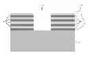
FIG. 5 schematically illustrates a hardmask layer of FIGS. 1 through 4 patterned to expose an area to be etched, in accordance with an exemplary embodiment.
DETAILED DESCRIPTION
In the following description, for the purposes of explanation, numerous specific details are set forth in order to provide a thorough understanding of exemplary embodiments. It should be apparent, however, that exemplary embodiments may be practiced without these specific details or with an equivalent arrangement. In other instances, well-known structures and devices are shown in block diagram form in order to avoid unnecessarily obscuring exemplary embodiments. In addition, unless otherwise indicated, all numbers expressing quantities, ratios, and numerical properties of ingredients, reaction conditions, and so forth used in the specification and claims are to be understood as being modified in all instances by the term “about.”
The present disclosure addresses and solves the current problem of poor etch resistance attendant upon etching semiconductor patterns therethrough. In accordance with embodiments of the present disclosure, a hardmask layer is formed by depositing alternating nanolayers of TiN with alternating residual stresses resulting in a hardmask layer with a net residual stress lower than either of the nanolayers and an increased hardness and etch resistance.
Methodology in accordance with embodiments of the present disclosure includes depositing a first nanolayer of TiN, and depositing a second nanolayer of TiN on the first nanolayer, wherein the first and second nanolayers have different residual stresses. The different residual stresses may be obtained by depositing the first and second nanolayers at different powers, different gas flow rates, or a combination thereof. The nanolayers may form a hardmask layer on an ILD, and the hardmask layer may be subsequently patterned to expose areas of the ILD to be etched.
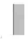
Adverting to FIG. 1, a method of forming a hardmask layer having nanolayers of varying residual stresses, in accordance with an exemplary embodiment, begins with a base layer 101. The base layer 101 may be any type of layer that may subsequently have a hardmask layer deposited on it or over it, such as an ILD in the manufacturing of a semiconductor device. The hardmask layer may be deposited directly on the base layer 101, or may be deposited over one or more additional layers between the hardmask layer and the base layer 101, depending on the specifics of the process.
Next, a first nanolayer 201 of TiN may be deposited over the base layer 101 to a thickness of less than or equal to 10 nanometers (nm), as illustrated in FIG. 2. The first nanolayer 201 may be deposited to have a first residual stress. The first residual stress may be controlled by depositing the first nanolayer 201 at a first power, such as 9 to 25 kW. Alternatively, the first residual stress may be controlled by depositing the first nanolayer 201 at a first gas flow rate of nitrogen (N2). Alternatively, the first residual stress may be controlled by depositing the first nanolayer 201 at a combination of the first power and the first gas flow rate.
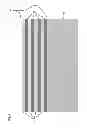
Adverting to FIG. 3, a second nanolayer 301 of TiN may be deposited over the first nanolayer 201 to a thickness of less than or equal to 10 nm. The second nanolayer 301 may be deposited to have a second residual stress, where the second residual stress is different than the first residual stress of the first nanolayer 201. The second residual stress is a function of depositing the second nanolayer 301 at a second power of 9 to 25 kW, and where the second power is different than the first power. Further, the first and second powers (and consequently the stresses) may be reversed. Thus, where the first power is, for example, 9 kW to deposit the first nanolayer 201, the second power to deposit the second nanolayer 301 may be, for example, 23 kW. Alternatively, the first power to deposit the first nanolayer 201 may be 23 kW, and the second power to deposit the second nanolayer 301 may be 9 kW.
Alternatively, the second residual stress may be controlled by depositing the second nanolayer 301 at a second gas flow rate of N2, where the second gas flow rate is different than the first gas flow rate, such as where the second gas flow rate is higher than the first gas flow rate. Alternatively, the first and second gas flow rates (and consequently the stresses) may be reversed. Thus, the second gas flow rate may be lower than the first gas flow rate.
Alternatively, the second residual stress may be controlled by depositing the second nanolayer 301 at a different power and a different gas flow rate compared to the first nanolayer 201. Indeed, the powers and the gas flow rates may be controlled to maximize the number of interfaces of the first and second nanolayers 201 and 301.
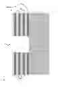
As illustrated in FIG. 4, subsequent alternating first and second nanolayers 201 and 301 may be deposited on the second nanolayer 301 to form a hardmask layer 401. The subsequent first and second nanolayers 201 and 301 may be formed by depositing the TiN while pulsing the power and/or the gas flow rate between the two powers, the two gas flow rates, or a combination thereof, as discussed above. Thus, the first and second nanolayers 201 and 301 may be repeatedly deposited N times, where N may be 1 to 150. By controlling the number of nanolayers 201 and 301, thereby controlling the number of interfaces between the nanolayers 201 and 301, as the residual stress builds in each nanolayer 201 and 301, vacancies created in the nanolayers 201 and 301 can diffuse between the interfaces to minimize the net stress of the film 401.
The hardmask layer 401 may be formed to a thickness of 1 to 10 nm and may include 2 to 300 interfaces of the first and second nanolayers 201 and 301. By forming the hardmask layer 401 of the alternating first and second nanolayers 201 and 301 with alternating residual stresses, the hardmask layer 401 may have a lower residual stress than either of the first and second nanolayers 201 and 301. The lower residual stress of the hardmask layer 401 provides enhanced hardness and etch resistance allowing the hardmask layer 401 to be used in trench first metal hardmask schemes, VIA double patterning schemes, and merged VIAs, where previous conventional hardmask layers may have failed.
Adverting to FIG. 5, the hardmask layer 401 may be subsequently patterned to form an opening 501 to form a metal pattern and/or a VIA pattern above the base layer 101 so that the base layer 101 may be subsequently etched. Based on the lower residual stress and increased hardness provided by the nanolayers of alternating residual stresses caused by pulsing the power and/or gas flow rate during the deposition, the hardmask layer 401 exhibits better etch resistance than a conventional hardmask layer.
The embodiments of the present disclosure achieve several technical effects, including providing a hardmask layer with lower residual stress and increased etch resistance such that the hardmask layer may be used in first metal hardmask schemes and VIA double patterning schemes. Embodiments of the present disclosure enjoy utility in various industrial applications as, for example, microprocessors, smart phones, mobile phones, cellular handsets, set-top boxes, DVD recorders and players, automotive navigation, printers and peripherals, networking and telecom equipment, gaming systems, and digital cameras. The present disclosure therefore enjoys industrial applicability in any of various types of highly integrated semiconductor devices.
In the preceding description, the present disclosure is described with reference to specifically exemplary embodiments thereof. It will, however, be evident that various modifications and changes may be made thereto without departing from the broader spirit and scope of the present disclosure, as set forth in the claims. The specification and drawings are, accordingly, to be regarded as illustrative and not as restrictive. It is understood that the present disclosure is capable of using various other combinations and embodiments and is capable of any changes or modifications within the scope of the inventive concept as expressed herein.
Claims
What is claimed is:1. A method comprising:
depositing a first nanolayer of titanium nitride (TiN); and
depositing a second nanolayer of TiN on the first nanolayer,
wherein the first and second nanolayers have different residual stresses.
2. A method according to claim 1, comprising depositing the first and second nanolayers at different powers, different gas flow rates, or a combination thereof to obtain the different residual stresses.
3. A method according to claim 1, comprising:
depositing the first nanolayer at a first power of 9 to 25 kilowatts (kW); and
depositing the second nanolayer at a second power of 9 to 25 kW, wherein the second power is different than the first power.
4. A method according to claim 1, comprising:
depositing the first nanolayer at a first gas flow rate of nitrogen (N2); and
depositing the second nanolayer at a second gas flow rate of N2, wherein the second gas flow rate is different than the first gas flow rate.
5. A method according to claim 1, further comprising depositing additional first and second nanolayers, alternating, on the second nanolayer, to form a film having a thickness of 1 to 10 nm.
6. A method according to claim 5, comprising forming each of the first and second nanolayers to a thickness of less than or equal 10 nanometer (nm).
7. A method according to claim 1, further comprising depositing additional first and second nanolayers, alternating, on the second nanolayer to form a film having 2 to 300 nanolayer interfaces.
8. A method according to claim 1, comprising depositing the first and second nanolayers on an interlayer dielectric (ILD) to form a hardmask layer.
9. A method according to claim 1, further comprising patterning the hardmask layer to expose areas to be etched.
10. A device comprising:
a substrate; and
a film comprising a first nanolayer of titanium nitride (TiN) having a first residual stress above the substrate, and a second nanolayer of TiN having a second residual stress on the first nanolayer,
wherein the first residual stress is different than the second residual stress.
11. A device according to claim 10, wherein a net residual stress of the film is less than the first residual stress and less than the second residual stress.
12. A device according to claim 10, wherein the film comprises multiple first and second nanolayers alternating.
13. A device according to claim 12, wherein the film comprises 2 to 300 nanolayer interfaces.
14. A device according to claim 12, wherein each of the first nanolayer and the second nanolayer have a thickness of less than or equal to 10 nm.
15. A device according to claim 10, wherein an etch resistance of the film is greater than an etch resistance of the first or second nanolayer.
16. A method comprising:
depositing a plurality of first nanolayers of titanium nitride (TiN) at a first power and a first gas flow rate over a substrate; and
depositing a plurality of second nanolayers of TiN, alternating with the first nanolayers, at a second power, different than the first power, and a second gas flow rate, different than the first gas flow rate, each second layer being deposited on a different first nanolayer,
wherein the first and second nanolayers form a film having 2 to 300 nanolayer interfaces.
17. A method according to claim 16, wherein each of the first nanolayer and the second nanolayer have a thickness of less than or equal to 10 nm.
18. A method according to claim 16, comprising:
depositing the first nanolayers at a first power of 9 to 25 kW; and
depositing the second nanolayers at a second power of 9 to 25 kW,
wherein the second power is different than the first power.
19. A method according to claim 16, comprising:
depositing the first nanolayers at a first gas flow rate of nitrogen N2; and
depositing the second nanolayers at a second gas flow rate of N2,
wherein the second gas flow rate is different than the first gas flow rate.
20. A method according to claim 16, comprising:
forming the film on an interlayer dielectric (ILD) over a substrate to form a hardmask; and
patterning the film to form openings for a metal pattern and vertical interconnect accesses (VIAs) to be etched.
Images & Drawings included:


Sources:
- United States Patent and Trademark Office - verify current appl. status at the USPTO↗
Recent applications in this class:
- » 20250266258 2025-08-21
SEMICONDUCTOR MEMORY DEVICE MANUFACTURING METHOD - » 20250246430 2025-07-31
METHOD OF MANUFACTURING A SEMICONDUCTOR DEVICE - » 20250246429 2025-07-31
Pattern Forming Method And Laminate - » 20250226223 2025-07-10
SUBSTRATE PROCESSING METHOD AND SUBSTRATE PROCESSING SYSTEM - » 20250226222 2025-07-10
SUBSTRATE PROCESSING METHOD AND SUBSTRATE PROCESSING SYSTEM - » 20250218773 2025-07-03
AMORPHOUS CARBON FILM AND DEPOSITION METHOD THEREOF - » 20250201557 2025-06-19
METHODS OF FORMING A BILAYER HARDMASK AND ASSOCIATED DEPOSITION METHODS USING A BILAYER HARDMASK - » 20250157819 2025-05-15
METHOD FOR PROCESSING A SUBSTRATE - » 20250132158 2025-04-24
USE OF TIN THIN FILM FOR BONDING AND AS MASKING FILM - » 20250132157 2025-04-24
HIGH SELECTIVITY DOPED HARDMASK FILMS
Recent applications for this Assignee:
- » 20220238386 2022-07-28
METHODS, APPARATUS, AND MANUFACTURING SYSTEM FOR SELF-ALIGNED PATTERNING OF A VERTICAL TRANSISTOR - » 20220200636 2022-06-23
Multiband receivers for millimeter wave devices - » 20220085994 2022-03-17
Public-private encryption key generation using Pcell parameter values and on-chip physically unclonable function values - » 20210066503 2021-03-04
Body-contacted field effect transistors configured for test and methods - » 20210063531 2021-03-04
Transmitter unit suitable for millimeter wave devices - » 20210057592 2021-02-25
Semiconductor detectors with butt-end coupled waveguide and method of forming the same - » 20210043727 2021-02-11
Gate-all-around field effect transistors with robust inner spacers and methods - » 20210027005 2021-01-28
Method, apparatus and system for wide metal line for SADP routing - » 20210005601 2021-01-07
Fin-type field effect transistor with reduced fin bulge and method - » 20210005454 2021-01-07
Metal on metal multiple patterning