LCD panel with anti-electrostatic discharge function and LCD device using same
US20140139792A1
2014-05-22
13/704,991
2012-11-23
✅ Patent granted
US 9,250,489 B2
2016-02-02
WO; PCT/CN2012/085094; 20121123
WO; WO2014/075331; 20140522
Paisley L Arendt
2033-06-09
Abstract:
The present disclosure provides a liquid crystal display (LCD) panel, and an LCD device. The LCD panel includes a color filter (CF) substrate, and an array substrate. A side of the CF substrate protrudes relative to the array substrate so that at least part of a common electrode of the CF substrate are exposed to the outside, and the common electrode of the CF substrate is electrically connected with a common line of the array substrate by a conducting member. The array substrate is further configured with a ground line, and discharge points are arranged between the common line of the array substrate and the ground line of the array substrate.
Assignee:
- SHENZHEN CHINA STAR OPTOELECTRONICS TECHNOLOGY CO., LTD. 1,397 🇨🇳 Shenzhen, China
Applicant:
Interested in similar patents?
Get notified when new applications in this technology area are published.
Classification:
G02F1/1343 » CPC main
Devices or arrangements for the control of the intensity, colour, phase, polarisation or direction of light arriving from an independent light source, e.g. switching, gating or modulating; Non-linear optics for the control of the intensity, phase, polarisation or colour based on liquid crystals, e.g. single liquid crystal display cells; Constructional arrangements; Operation of liquid crystal cells; Circuit arrangements; Constructional arrangements; Manufacturing methods Electrodes
G02F1/136204 » CPC main
Devices or arrangements for the control of the intensity, colour, phase, polarisation or direction of light arriving from an independent light source, e.g. switching, gating or modulating; Non-linear optics for the control of the intensity, phase, polarisation or colour based on liquid crystals, e.g. single liquid crystal display cells; Constructional arrangements; Operation of liquid crystal cells; Circuit arrangements; Liquid crystal cells structurally associated with a semi-conducting layer or substrate, e.g. cells forming part of an integrated circuit; Active matrix addressed cells Arrangements to prevent high voltage or static electricity failures
G02B6/4275 » CPC further
Light guides; Coupling light guides; Coupling light guides with opto-electronic elements; Packages, e.g. shape, construction, internal or external details; Electrical aspects Protection against electrostatic discharge [ESD]
H01L23/5286 » CPC further
Details of semiconductor or other solid state devices; Arrangements for conducting electric current within the device in operation from one component to another, i.e. interconnections, e.g. wires, lead frames including external interconnections consisting of a multilayer structure of conductive and insulating layers inseparably formed on the semiconductor body layout of the interconnection structure Arrangements of power or ground buses
H01L27/0248 » CPC further
Devices consisting of a plurality of semiconductor or other solid-state components formed in or on a common substrate including semiconductor components specially adapted for rectifying, oscillating, amplifying or switching and having at least one potential-jump barrier or surface barrier; including integrated passive circuit elements with at least one potential-jump barrier or surface barrier; Particular design considerations for integrated circuits for electrical or thermal protection, e.g. electrostatic discharge [ESD] protection
H01L2224/8511 » CPC further
Indexing scheme for arrangements for connecting or disconnecting semiconductor or solid-state bodies and methods related thereto as covered by; Methods for connecting semiconductor or other solid state bodies using means for bonding being attached to, or being formed on, the surface to be connected using a wire connector involving protection against electrical discharge, e.g. removing electrostatic charge
G02F1/1362 IPC
Devices or arrangements for the control of the intensity, colour, phase, polarisation or direction of light arriving from an independent light source, e.g. switching, gating or modulating; Non-linear optics for the control of the intensity, phase, polarisation or colour based on liquid crystals, e.g. single liquid crystal display cells; Constructional arrangements; Operation of liquid crystal cells; Circuit arrangements; Liquid crystal cells structurally associated with a semi-conducting layer or substrate, e.g. cells forming part of an integrated circuit Active matrix addressed cells
G02F1/1345 » CPC further
Devices or arrangements for the control of the intensity, colour, phase, polarisation or direction of light arriving from an independent light source, e.g. switching, gating or modulating; Non-linear optics for the control of the intensity, phase, polarisation or colour based on liquid crystals, e.g. single liquid crystal display cells; Constructional arrangements; Operation of liquid crystal cells; Circuit arrangements; Constructional arrangements; Manufacturing methods Conductors connecting electrodes to cell terminals
G02B6/42 IPC
Light guides; Coupling light guides Coupling light guides with opto-electronic elements
H01L23/528 IPC
Details of semiconductor or other solid state devices; Arrangements for conducting electric current within the device in operation from one component to another, i.e. interconnections, e.g. wires, lead frames including external interconnections consisting of a multilayer structure of conductive and insulating layers inseparably formed on the semiconductor body layout of the interconnection structure
H01L23/60 » CPC further
Details of semiconductor or other solid state devices; Structural electrical arrangements for semiconductor devices not otherwise provided for, e.g. in combination with batteries Protection against electrostatic charges or discharges, e.g. Faraday shields
H01L27/02 IPC
Devices consisting of a plurality of semiconductor or other solid-state components formed in or on a common substrate including semiconductor components specially adapted for rectifying, oscillating, amplifying or switching and having at least one potential-jump barrier or surface barrier; including integrated passive circuit elements with at least one potential-jump barrier or surface barrier
Description
TECHNICAL FIELD
The present disclosure relates to the field of a liquid crystal display (LCD), and more particularly to an LCD panel and an LCD device.
BACKGROUND
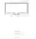
As shown in FIG. 1 and FIG. 2, a liquid crystal display (LCD) panel in the prior art mainly includes three layers: a color filter (CF) substrate 1, an array substrate 2, and a liquid crystal (LC) layer 3. Generally, most circuits of the LCD panel are arranged on the array substrate 2, thus, the CF substrate 1 and the array substrate 2 are arranged in a staggered mode, and the array substrate 2 protrudes relative to the CF substrate 1 so that some circuits of the array substrate 2 are exposed to the outside. The exposed circuits of the array substrate 2 are laminated and interconnect with an external flexible printed circuit (FPC) 4. A transparent conducting layer (also called common electrode layer 11) of the CF substrate is interconnected with a common line of the array substrate by a conducting ball (Au ball).
In order to reduce cost, manufacturers of the LCD panel often hope to cut LCD panels having more of a bigvisible area using a glass substrate having a certain size, which results in less space of the LCD panel used to locate components. In order to ensure reliability of the LCD panel, a common method is to protrude a side of the CF substrate relative to the array substrate to locate components. As shown in FIG. 2, because the staggered arrangement causes a part of the transparent conducting layer of the CF substrate 1 to be exposed to the outside, the exposed part of the transparent conducting layer may be easily affected by electrostatic discharge (ESD), and circuits and related integrated chips (ICs) may be burnt out in severe cases. Because there is no etching process in a manufacturing process of the CF substrate, eliminating influence of ESD on the exposed the transparent conducting layer of the CF substrate becomes a difficult problem for engineers. One method used at present is to coat the exposed transparent conducting layer of the CF substrate with an insulating glue for protection which may increase cost and work time.
SUMMARY
In view of the above-described problems, the aim of the present disclosure is to provide a liquid crystal display (LCD) panel and an LCD device thereof with the advantages of low cost, high electro-static discharge (ESD) interference resistance, and long service life.
A first technical scheme of the present disclosure is that: an LCD panel comprises a color filter (CF) substrate and an array substrate. A side of the CF substrate protrudes relative to the array substrate so that at least part of a common electrode of the CF substrate is exposed to the outside. The common electrode of the CF substrate is electrically connected with a common line of the array substrate by a conducting member. The array substrate is further configured with a ground line, and a plurality pairs of discharge points are arranged between the common line of the array substrate and the ground line of the array substrate. The discharge points are arranged alongside the conducting member, and the conducting member is a conducting ball (Au ball). The ground line is arranged inside the common line of the array substrate, and the ground line is arranged in parallel with the common line. A side of the array substrate protrudes relative to the CF substrate so that at least some circuits of the array substrate are exposed to the outside. The exposed circuits of the array substrate 2 are laminated and interconnect with an external flexible printed circuit (FPC). The discharge points are arranged in an area adjacent to two ends of a laminated area and an area opposite to the laminated area.
A second technical scheme of the present disclosure is that: an LCD panel comprises a CF substrate and an array substrate. A side of the CF substrate protrudes relative to the array substrate so that at least part of a common electrode of the CF substrate is exposed to the outside. The common electrode of the CF substrate is electrically connected with the common line of the array substrate by a conducing member, the array substrate is further configured with a ground line, and discharge points are arranged between the common line of the array substrate and the ground line of the array substrate.
In one example, the number of pairs of discharge points between the common line of the array substrate and the ground line of the array substrate are two or more.
In one example, the discharge points are arranged alongside the conducting member. Because the common electrode is electrically connected with the common line by the conducting member, the discharge points should be arranged alongside the conducting member. Thus, electrostatic charges can be transferred to the common line from the common electrode at a short distance.
In one example, the conducting member is a conducting ball (Au ball).
In one example, the ground line is arranged inside the common line of the array substrate, and the ground line is arragned in parallel with the common line. Thus, the discharge points can be arranged at any location of the ground line and the common line to quickly discharge electrostatic charges at a short distance.
In one example, a side of the array substrate protrudes relative to the CF substrate so that at least some circuits of the array substrate are exposed to the outside. The exposed circuits of the array substrate 2 are laminated and interconnect with the external FPC. The discharge points are arranged in an area adjacent to two ends of a laminated area and an area opposite to the laminated area.
A third technical scheme of the present disclosure is that: an LCD device comprises the LCD panel mentioned above.
Advantages of the present disclosure are summarized below: in the LCD panel of the present disclosure, because a side of the CF substrate protrudes relative to the array substrate, at least part of a common electrode of the CF substrate is exposed to the outside, and the exposed part of the common electrode is easily affected by ESD. However, the LCD panel has bigger space used to locate components, which is a trend of narrower frame design. In the present disclosure, by arranging the discharge points between the common line of the array substrate and the ground line of the array substrate, when the exposed part of the common electrode of the CF substrate is affected by ESD, the electrostatic charges are transferred to the common line of the array substrate by the conducting member and discharge points discharge between the common line and the ground line. The electrostatic charges are transferred to the ground line and then flow into earth and is completely discharged which protects electrostatic, increases the ESD interference resistance of the LCD panel, reduce the production defect rate, and increases the service life. The ground line can be a newly added ground line, and can be an original ground line moved adjacent to the common line. The discharge points are easily arranged, and are manufactured in the etching process of manufacturing the common line of the array substrate and the ground line of the array substrate without increasing manufacture cost and work time basically.
BRIEF DESCRIPTION OF FIGURES
FIG. 1 is a structural diagram of a liquid crystal display (LCD) panel in the prior art;
FIG. 2 is a sectional view of an LCD panel in the prior art;
FIG. 3 is a structural diagram of an example of an LCD panel of the present disclosure; and
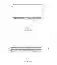
FIG. 4 is an enlarged view of a discharge point shown in FIG. 3.
DETAILED DESCRIPTION
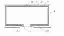
The present disclosure provides a liquid crystal display (LCD) device, comprising an LCD panel. FIG. 3 and FIG. 4 show an example of the LCD panel of the present disclosure. The LCD panel comprises a color filter (CF) substrate 1 and an array substrate 2. A side of the array substrate 2 protrudes relative to the CF substrate 1 so that at least some circuits of the array substrate 2 are exposed to the outside. The exposed circuits of the array substrate are laminated and interconnect with an external flexible printed circuit (FPC) 4. A side of the CF substrate 1 protrudes relative to the array substrate 2 so that at least part of a common electrode 11 of the CF substrate 1 is exposed to the outside. The common electrode 11 of the CF substrate 1 is electrically connected with a common line 21 of the array substrate 2 by a conducting member 6. The array substrate 2 is further configured with a ground line 22, and discharge points 23 are arranged between the common line 21 of the array substrate 2 and the ground line 22 of the array substrate 2.
In the LCD panel of the present disclosure, because the side of the CF substrate 1 protrudes relative to the array substrate 2, a part of the common electrode 11 of the CF substrate 1 is exposed to the outside, and the exposed part of the common electrode 11 of the CF substrate 1 is easily affected by electro-static discharge (ESD). However, the LCD panel has more space used to accomodate components, which is a trend of narrower frame design. In the present disclosure, by arranging the discharge points 23 between the common line 21 of the array substrate 2 and the ground line 22 of the array substrate 2, when the exposed part of the common electrode 11 of the CF substrate is affected by ESD, the electrostatic charges are transferred to the common line 21 of the array substrate 2 by the conducting member 6, and discharge points 23 discharge between the common line 21 and the ground line 22. The electrostatic charges are transferred to the ground line 22 and then flow into ground and is completely discharged. The discharging protects electrostatics, increases ESD interference resistance of the LCD panel, reduces defect rates of production, and increases service life. The ground line 22 can be a newly added ground line, and also can be an original ground line moved adjacent to the common line. The discharge points 23 are easily arranged, and are manufactured in an etching process when the common line of the array substrate and the ground line of the array substrate is manufactured without increasing manufacture cost and work time.
In the example, the conducting member 6 is a conducting ball (Au ball), where one end of the conducting ball is connected with the common electrode of the CF substrate, and the other end is connected with the common line of the array substrate. In principle, the discharge points should be arranged adjacent to the position where is easily affected by ESD. Because the common electrode 11 is electrically connected with the common line 21 by the conducting member 6, the discharge points 23 should be arranged alongside the conducting member 6. Thus, the electrostatic charges can be transferred to the common line 21 from the common electrode 11 at a short distance.
In the example, there are a plurality pairs of discharge points 23 between the common line 21 of the array substrate 2 and the ground line 22 of the array substrate 2. Because if only one pair of discharge points are arranged, sharpness of the discharge points may be damaged by multiple discharge, thereby resulting in sharp corner passivation and affecting effect of discharging of the discharge points which can be avoided by arranging a plurality pairs of discharge points.
In the example, the ground line 22 is arranged inside the common line 21 of the array substrate 2, and the ground line 22 is arranged in parallel with the common line 21. Thus, the discharge points 23 can be arranged at any location of the ground line 22 and the common line 21 to quickly discharge electrostatic charges at a short distance.
In the present disclosure, because the conducting members 6 in the prior art are arranged on a upper side and a lower side of the LCD panel in general, the discharge points 23 should be arranged on the upper side of the array substrate 2 and the lower side of the array substrate 2. Specifically, the discharge points 23 are arranged in an area adjacent to the two ends of a laminated area 5 and an area opposite to the laminated area 5. If arrangement of the areas used to arrange the discharge points 23 are reasonable, the ESD distance is short, and actual effect of the discharge can be improved.
The present disclosure is described in detail in accordance with the above contents with the specific preferred examples. However, this present disclosure is not limited to the specific examples. For the ordinary technical personnel of the technical field of the present disclosure, on the premise of keeping the conception of the present disclosure, the technical personnel can also make simple deductions or replacements, and all of which should be considered to belong to the protection scope of the present disclosure.
Claims
1. A liquid crystal display (LCD) panel, comprising:
a color filter (CF) substrate, and
an array substrate; wherein a side of the CF substrate protrudes relative to the array substrate so that at least part of a common electrode of the CF substrate is exposed to the outside; the common electrode of the CF substrate is electrically connected with a common line of the array substrate by a conducting member;
wherein the array substrate is further configured with a ground line, and a plurality pairs of discharge points are arranged between the common line of the array substrate and the ground line of the array substrate; the discharge points are arranged alongside the conducting member, and the conducting member is a conducting ball; the ground line is arranged inside the common line of the array substrate, and the ground line is arranged in parallel with the common line;
wherein a side of the array substrate protrudes relative to the CF substrate so that at least some circuits of the array substrate are exposed to the outside, wherein the exposed circuits of the array substrate are laminated and interconnect with an external flexible printed circuit (FPC); the discharge points are arranged in an area adjacent to two ends of a laminated area and an area opposite to the laminated area.
2. A liquid crystal display (LCD) panel, comprising:
a color filter (CF) substrate, and
an array substrate; wherein a side of the CF substrate protrudes relative to the array substrate so that at least part of a common electrode of the CF substrate is exposed to the outside, and the common electrode of the CF substrate is electrically connected with a common line of the array substrate by a conducting member; the array substrate is further configured with a ground line, and discharge points are arranged between the common line of the array substrate and the ground line of the array substrate.
3. The liquid crystal display (LCD) panel of claim 2, wherein the number of pairs of discharge points between the common line of the array substrate and the ground line of the array substrate are two or more.
4. The liquid crystal display (LCD) panel of claim 2, wherein the discharge points are arranged alongside the conducting member.
5. The liquid crystal display (LCD) panel of claim 2, wherein the conducting member is a conducting ball.
6. The liquid crystal display (LCD) panel of claim 2, wherein the ground line is arranged inside the common line of the array substrate, and the ground line is arranged in parallel with the common line.
7. The liquid crystal display (LCD) panel of claim 2, wherein a side of the array substrate protrudes relative to the CF substrate so that at least some circuits of the array substrate are exposed to the outside to be laminated and interconnect to the external flexible printed circuit (FPC); the discharge points are arranged in an area adjacent to two ends of a laminated area and an area opposite to the laminated area.
8. A liquid crystal display (LCD) device, comprising:
an LCD panel comprising a color filter (CF) substrate and an array substrate; a side of the CF substrate protrudes relative to the array substrate so that at least part of a common electrode of the CF substrate is exposed to the outside, and the common electrode of the CF substrate is electrically connected with a common line of the array substrate by a conducting member; the army substrate is further configured with a ground line, and discharge points are arranged between the common line of the array substrate and the ground line of the array substrate.
9. The liquid crystal display (LCD) device of claim 8, wherein the number of pairs of discharge points between the common line of the array substrate and the ground line of the array substrate are two or more.
10. The liquid crystal display (LCD) device of claim 8, wherein the discharge points are arranged alongside the conducting member.
11. The liquid crystal display (LCD) device of claim 8, wherein the ground line is arranged inside the common line of the array substrate, and the ground line is arranged in parallel with the common line.
12. The liquid crystal display (LCD) device of claim 8, wherein the conducting member is a conducting ball.
13. The liquid crystal display (LCD) device of claim 8, wherein a side of the array substrate protrudes relative to the color filter (CF) substrate so that at least some circuits of the array substrate are exposed to the outside. The exposed circuits of the array substrate are laminated and interconnect with the external (flexible printed circuit) FPC; the discharge points are arranged in an area adjacent to two ends of a laminated area and an area opposite to the laminated area.
Images & Drawings included:
Sources:
- United States Patent and Trademark Office - verify current appl. status at the USPTO↗
Recent applications in this class:
- » 20250271707 2025-08-28
Light Modulation Module and Driving Method Thereof, Display Apparatus, and Light-Emitting Apparatus - » 20250020960 2025-01-16
DISPLAY DEVICE - » 20240337881 2024-10-10
LIQUID CRYSTAL DISPLAY DEVICE AND ELECTRONIC APPLIANCE - » 20240210764 2024-06-27
LIQUID CRYSTAL LENS, DRIVING METHOD, EYEGLASSES, ELECTRONIC PRODUCT, VR DEVICE, AND AR DEVICE - » 20240184168 2024-06-06
DISPLAY PANEL, DISPLAY DEVICE, INPUT/OUTPUT DEVICE, AND DATA PROCESSING DEVICE - » 20240061293 2024-02-22
DISPLAY DEVICE - » 20240061292 2024-02-22
Display device - » 20240045276 2024-02-08
OPTICAL DEVICE - » 20240036403 2024-02-01
Array substrate, liquid crystal display panel, and display device having trapezoidal shaped electrode - » 20230205020 2023-06-29
DISPLAY DEVICE
Recent applications for this Assignee:
- » 20220052204 2022-02-17
Amorphous silicon thin film transistor and method for manufacturing the same - » 20210405424 2021-12-30
Array substrate - » 20210358953 2021-11-18
Pixel structure, array substrate, and display device - » 20210336040 2021-10-28
Manufacturing method of TFT substrate - » 20210335832 2021-10-28
Thin film transistor (TFT) array substrate and display panel - » 20210191204 2021-06-24
Pixel structure and display panel containing same - » 20210090528 2021-03-25
Display driving system - » 20210083229 2021-03-18
OLED display panel and manufacturing method thereof - » 20210083010 2021-03-18
Color filter substrate having a filter layer disposed on quantum dot layer - » 20210082358 2021-03-18
White balance method and device for LCD panel