Method and device of a LED matrix
US20140209942A1
2014-07-31
14/241,187
2012-08-29
✅ Patent granted
US 9,232,663 B2
2016-01-05
WO; PCT/IB2012/054436; 20120829
WO; WO2013/035017; 20130314
Jamie C Niesz
Meenakshy Chakravorty
2032-08-29
Abstract:
There is provided a method for manufacturing a light emitting diode, LED, matrix (100) comprising the steps of providing with a maintained integrity a conductor sheet (150) with a plurality of component areas (111) interconnected with meandering connection tracks (116), mounting a plurality of LEDs (120) to a respective component area thereby forming a subassembly (100″), trimming and stretching the subassembly thereby straightening the connection tracks such that an m×n LED conductor matrix is formed during the step of stretching.
Inventors:
- Antonius Petrus Marinus Dingemans 13 🇳🇱 Tilburg, Netherlands
- Johannes Wilhelmus Weekamp 51 🇳🇱 Beek En Donk, Netherlands
- Giovanni Cennini 33 🇳🇱 Eindhoven, Netherlands
- Gerard Kums 6 🇧🇪 Molenstede, Belgium
- Sébastien Paul René Libon 5 🇧🇪 Tervuren, Belgium
Assignee:
- Koninklijke Philips N.V. 10,434 🇳🇱 Eindhoven, Netherlands
Applicant:
Interested in similar patents?
Get notified when new applications in this technology area are published.
Classification:
H01L27/153 » CPC main
Devices consisting of a plurality of semiconductor or other solid-state components formed in or on a common substrate including semiconductor components with at least one potential-jump barrier or surface barrier specially adapted for light emission in a repetitive configuration, e.g. LED bars
H01L27/15 IPC
Devices consisting of a plurality of semiconductor or other solid-state components formed in or on a common substrate including semiconductor components with at least one potential-jump barrier or surface barrier specially adapted for light emission
H01L33/62 » CPC further
Semiconductor devices with at least one potential-jump barrier or surface barrier specially adapted for light emission; Processes or apparatus specially adapted for the manufacture or treatment thereof or of parts thereof; Details thereof characterised by the semiconductor body packages Arrangements for conducting electric current to or from the semiconductor body, e.g. lead-frames, wire-bonds or solder balls
H05K2201/09263 » CPC further
Indexing scheme relating to printed circuits covered by; Shape and layout; Shape and layout details of conductors; Conductive traces Meander
H05K2201/09263 » CPC further
Indexing scheme relating to printed circuits covered by; Shape and layout; Shape and layout details of conductors; Conductive traces Meander
H05K3/303 » CPC main
Apparatus or processes for manufacturing printed circuits; Assembling printed circuits with electric components, e.g. with resistor Surface mounted components, e.g. affixing before soldering, aligning means, spacing means
H05K3/303 » CPC main
Apparatus or processes for manufacturing printed circuits; Assembling printed circuits with electric components, e.g. with resistor Surface mounted components, e.g. affixing before soldering, aligning means, spacing means
F21K9/90 » CPC further
Light sources using semiconductor devices as light-generating elements, e.g. using light-emitting diodes [LED] or lasers Methods of manufacture
F21V21/002 » CPC further
Supporting, suspending, or attaching arrangements for lighting devices ; Hand grips making direct electrical contact, e.g. by piercing
H01L25/0753 » CPC further
Assemblies consisting of a plurality of individual semiconductor or other solid state devices ; Multistep manufacturing processes thereof all the devices being of a type provided for in the same subgroup of groups - , e.g. assemblies of rectifier diodes the devices not having separate containers the devices being of a type provided for in group the devices being arranged next to each other
H05K1/0283 » CPC further
Printed circuits; Details; Bendability or stretchability details Stretchable printed circuits
H05K1/0283 » CPC further
Printed circuits; Details; Bendability or stretchability details Stretchable printed circuits
H05K3/202 » CPC further
Apparatus or processes for manufacturing printed circuits in which conductive material is applied to the insulating support in such a manner as to form the desired conductive pattern by affixing prefabricated conductor pattern using self-supporting metal foil pattern
H05K3/202 » CPC further
Apparatus or processes for manufacturing printed circuits in which conductive material is applied to the insulating support in such a manner as to form the desired conductive pattern by affixing prefabricated conductor pattern using self-supporting metal foil pattern
H05K13/046 » CPC further
Apparatus or processes specially adapted for manufacturing or adjusting assemblages of electric components; Mounting of components, e.g. of leadless components Surface mounting
H05K13/046 » CPC further
Apparatus or processes specially adapted for manufacturing or adjusting assemblages of electric components; Mounting of components, e.g. of leadless components Surface mounting
H01L2924/0002 » CPC further
Indexing scheme for arrangements or methods for connecting or disconnecting semiconductor or solid-state bodies as covered by; Technical content checked by a classifier Not covered by any one of groups , and
H05K1/0209 » CPC further
Printed circuits; Details; Thermal arrangements, e.g. for cooling, heating or preventing overheating; Cooling of mounted components External configuration of printed circuit board adapted for heat dissipation, e.g. lay-out of conductors, coatings
H05K1/0209 » CPC further
Printed circuits; Details; Thermal arrangements, e.g. for cooling, heating or preventing overheating; Cooling of mounted components External configuration of printed circuit board adapted for heat dissipation, e.g. lay-out of conductors, coatings
H05K1/0284 » CPC further
Printed circuits; Details Details of three-dimensional rigid printed circuit boards
H05K1/0284 » CPC further
Printed circuits; Details Details of three-dimensional rigid printed circuit boards
H05K3/0058 » CPC further
Apparatus or processes for manufacturing printed circuits Laminating printed circuit boards onto other substrates, e.g. metallic substrates
H05K3/0058 » CPC further
Apparatus or processes for manufacturing printed circuits Laminating printed circuit boards onto other substrates, e.g. metallic substrates
H05K3/0097 » CPC further
Apparatus or processes for manufacturing printed circuits Processing two or more printed circuits simultaneously, e.g. made from a common substrate, or temporarily stacked circuit boards
H05K3/0097 » CPC further
Apparatus or processes for manufacturing printed circuits Processing two or more printed circuits simultaneously, e.g. made from a common substrate, or temporarily stacked circuit boards
H05K2201/09781 » CPC further
Indexing scheme relating to printed circuits covered by; Shape and layout; Shape and layout details of conductors covering at least two types of conductors provided for in - Dummy conductors, i.e. not used for normal transport of current; Dummy electrodes of components
H05K2201/09781 » CPC further
Indexing scheme relating to printed circuits covered by; Shape and layout; Shape and layout details of conductors covering at least two types of conductors provided for in - Dummy conductors, i.e. not used for normal transport of current; Dummy electrodes of components
H05K2201/10106 » CPC further
Indexing scheme relating to printed circuits covered by; Details of components or other objects attached to or integrated in a printed circuit board; Types of components Light emitting diode [LED]
H05K2201/10106 » CPC further
Indexing scheme relating to printed circuits covered by; Details of components or other objects attached to or integrated in a printed circuit board; Types of components Light emitting diode [LED]
H05K2203/04 » CPC further
Indexing scheme relating to apparatus or processes for manufacturing printed circuits covered by Soldering or other types of metallurgic bonding
H05K2203/04 » CPC further
Indexing scheme relating to apparatus or processes for manufacturing printed circuits covered by Soldering or other types of metallurgic bonding
H05K2203/1545 » CPC further
Indexing scheme relating to apparatus or processes for manufacturing printed circuits covered by; Position of the PCB during processing Continuous processing, i.e. involving rolls moving a band-like or solid carrier along a continuous production path
H05K2203/1545 » CPC further
Indexing scheme relating to apparatus or processes for manufacturing printed circuits covered by; Position of the PCB during processing Continuous processing, i.e. involving rolls moving a band-like or solid carrier along a continuous production path
H05K2203/175 » CPC further
Indexing scheme relating to apparatus or processes for manufacturing printed circuits covered by; Post-manufacturing processes Configurations of connections suitable for easy deletion, e.g. modifiable circuits or temporary conductors for electroplating; Processes for deleting connections
Y10T29/49144 » CPC further
Metal working; Method of mechanical manufacture; Electrical device making; Conductor or circuit manufacturing; On flat or curved insulated base, e.g., printed circuit, etc.; Assembling to base an electrical component, e.g., capacitor, etc. by metal fusion
H01L21/00 IPC
Processes or apparatus adapted for the manufacture or treatment of semiconductor or solid state devices or of parts thereof
H05K3/30 IPC
Apparatus or processes for manufacturing printed circuits Assembling printed circuits with electric components, e.g. with resistor
H05K3/30 IPC
Apparatus or processes for manufacturing printed circuits Assembling printed circuits with electric components, e.g. with resistor
H05K3/20 IPC
Apparatus or processes for manufacturing printed circuits in which conductive material is applied to the insulating support in such a manner as to form the desired conductive pattern by affixing prefabricated conductor pattern
H05K3/20 IPC
Apparatus or processes for manufacturing printed circuits in which conductive material is applied to the insulating support in such a manner as to form the desired conductive pattern by affixing prefabricated conductor pattern
H01L25/075 IPC
Assemblies consisting of a plurality of individual semiconductor or other solid state devices ; Multistep manufacturing processes thereof all the devices being of a type provided for in the same subgroup of groups - , e.g. assemblies of rectifier diodes the devices not having separate containers the devices being of a type provided for in group
F21S4/00 IPC
Lighting devices or systems using a string or strip of light sources
H05K13/04 IPC
Apparatus or processes specially adapted for manufacturing or adjusting assemblages of electric components Mounting of components, e.g. of leadless components
H05K13/04 IPC
Apparatus or processes specially adapted for manufacturing or adjusting assemblages of electric components Mounting of components, e.g. of leadless components
H05K1/02 IPC
Printed circuits Details
H05K1/02 IPC
Printed circuits Details
H05K3/00 IPC
Apparatus or processes for manufacturing printed circuits
H05K3/00 IPC
Apparatus or processes for manufacturing printed circuits
Description
FIELD OF THE INVENTION
The present invention relates to the field of light emitting diode (LED) lighting devices, and more particularly to a method for manufacturing a light emitting diode, LED, matrix for large area LED lighting devices, and a corresponding lighting device.
BACKGROUND OF THE INVENTION
Light emitting diodes (LEDs) in large area lighting devices have been used for some time, where a large number of LEDs are arranged as an array or matrix to evenly provide lighting over a large area. Typically, LEDs have been arranged on a printed circuit board (PCB) by means of traditional surface mounting techniques. However, recently there has been proposed other types of solutions to provide large area LED arrays.
WO 2007/125566 A1 discloses a method for manufacturing a LED array in which N electrically conducting wires are arranged in parallel creating an array of wires having a width D perpendicular to the length direction of the wires. Further, LED components are arranged to the array of wires such that each LED component is electrically connected to at least two adjacent wires, and subsequently the array of wires is stretched such that the width of the array is increased. To connect to the wires, the LED components are each arranged with a printed circuit board or lead frame with snap locks, or by means of soldering, gluing, insulation displacement connection (IDC) or similar. The proposed method provides a low cost solution for applications where large lighting area is important. However, mounting of small components is difficult on wires, and the proposed method requires that the wires have to be placed on a temporary carrier which is removed after mounting of the components.
SUMMARY OF THE INVENTION
In view of the above, an object of the invention is to provide an alternative and improved method of manufacturing a LED array, and to at least alleviate the problems discussed above.
This object is achieved by a method for manufacturing a LED matrix according to the present invention as defined in claim 1. Thus, in accordance with an aspect of the present invention, there is provided a method for manufacturing a light emitting diode, LED, matrix comprising providing a first conductor structure having a plurality of component areas interconnected with meandering connection tracks by providing a conductor sheet with a first predetermined pattern, mounting a plurality of LEDs to a respective component area of the first conductor structure thereby forming a subassembly, trimming the subassembly to provide a second conductor structure, and stretching the subassembly thereby straightening the connection tracks. The second conductor structure is arranged such that an m×n conductor matrix is formed during the step of stretching. Thereby, there is provided an effective method to manufacture a large area LED matrix in which, in a first step, a conductor structure is provided from a conducting sheet material. The sheet material may advantageously be fed from a roll and the first conductor structure may be mechanically punched out while maintaining integrity of the conductor sheet. This allows for feeding the patterned conductor sheet into a standard soldering (or optionally gluing) pick and place process for mounting of the LEDs onto a respective component area. After trimming, e.g. by means of laser cutting, or punching and/or cutting, of the conductor sheet to release any integrity governing bridges, the conductor structure is stretched such that the meandering connection tracks are straightened and the large area matrix is formed. Thus, the method is suitable for a mechanical reel-to-reel process using standard component mounting facilities which is highly advantageous for producing large volumes at low cost. Further, by performing e.g. the mounting of the components in a high density set up, efficient time and space usage of the mounting facility is provided, while still providing a large area of the final LED matrix. A further advantage with the present concept, as compared to the prior art wire solution, is that LED's (or other components) having more than two connection pads are mountable on the subassembly, when the first predetermined pattern is adapted for such component.
In embodiments of the method, before stretching, additional coatings and/or optical elements are applied. Also bending the lead frame locally may be performed, which can be beneficial e.g. for changing the orientation of the LEDs.
According to an embodiment, the method further comprises arranging the stretched subassembly onto a substrate. By decoupling the production of the LED matrix from a traditional substrate (contrary to when using a PCB based LED matrix), the substrate onto which the LED matrix is mounted may be more freely chosen.
This substrate could act as reflector and in case of metal as additional heat sink According to an embodiment of the method, the first predetermined pattern is selected for providing at least one thermal pad area in the first or second conductor structure, which is advantageous for integrating predetermined areas with facilitated thermal dissipation into the LED conductor matrix.
According to an embodiment, at least one thermal pad area is arranged at a component area, or at a connection track. The area of the thermal pad is preferably selected to provide sufficient thermal dissipation to cool a LED or component at which it is arranged. According to an embodiment of the method (and the correspondingly produced LED conductor matrix and a lighting device in which the LED conductor matrix is arranged), the areas of thermal pads arranged at a LED or component are arranged to have different size on different sides of the component, which is advantageous e.g. when the component is asymmetrically dissipating heat, or in case one of the component/LED interconnect pads dissipate more heat than the other pad (due to material choice, position in the electrical design, position on the substrate etc.)
According to an embodiment, the method further comprises providing at least one recess in the component area for receiving LEDs or LED packages of a size less then 1×1×1 mm, which is advantageous. This is applicable for Wafer Level Chip Scale Package, WLCSP, which are expected to become the lowest cost package for LED's on the market.
According to an embodiment, the step of mounting comprises defining solder areas on the first conductor structure, applying solder onto the solder areas, placing the LEDs on a respective component area, and performing soldering, which is advantageous.
According to an embodiment, the first or second conductor structure is arranged with alignment features and/or stretch alignment features, like for instance holes.
According to an embodiment, the method further comprises providing mechanical deformation of the subassembly by means of one of splitting, trimming of the subassembly to a predetermined contour.
According to an embodiment, the method further comprises deforming at least one portion of the subassembly to provide a predetermined lighting direction of at least one LED. For instance, portions onto which specific LEDs are arranged may be bent to provide a predetermined lighting direction for the LEDs, thereby enabling the use of top emitting LEDs as side emitting LEDs.
According to an embodiment, the method further comprises providing deformation of the subassembly for providing one of: optical properties, mechanical fixation of the component interconnect board, mechanical fixation of additional components, thermal properties, and connector functionality.
According to an embodiment, at least one of providing the first predetermined pattern and the second conductor structure is done by means of etching, cutting, punching, slitting or laser cutting.
According to a second and third aspects of the invention, there is provided a LED matrix produced with a method according to the invention, and a large area lighting device comprising such a LED matrix. These have the same advantages as mentioned above with respect to the method, e.g. the decoupled processing of the circuitry before mounting to the substrate allows for providing lighting devices with more optimized substrates. Further, the LED matrix produced according to the present method can be made very large without requiring interconnect between sub portions of a matrix (compare for instance with large area lighting with the standard PCB solution, which either requires use of very large PCB's, which as previously mentioned still are limited in size and expensive to produce, or use of an array of PCB's with interconnect liners between the individual PCBs).
The described invention is broadly applicable in LED products but especially interesting for LED modules and lamps, which are really large measuring up to several m2. Other objectives, features and advantages will appear from the following detailed disclosure, from the attached dependent claims as well as from the drawings.
BRIEF DESCRIPTION OF THE DRAWINGS
The above, as well as additional objects, features and advantages of the present invention, will be better understood through the following illustrative and non-limiting detailed description of preferred embodiments of the present invention, with reference to the appended drawings, where the same reference numerals will be used for similar elements, wherein:
FIGS. 1a) to c) are schematic top views, and d) to e) are perspective views of a LED matrix according to the present invention during different steps of manufacturing;
FIGS. 2a) to b) are schematic illustrations of details of embodiments of a LED matrix according to the present invention; and
FIGS. 3a) to d) are schematic illustrations of manufacturing steps of a detail of an embodiment of a LED matrix according to the present invention.
DETAILED DESCRIPTION OF PREFERRED EMBODIMENTS
An exemplifying embodiment of the method for manufacturing a LED matrix according to the present invention is now described with reference to FIGS. 1a)-e). The steps of the method are described as a continuous sequence, however some of the steps may be performed in another order or some additional process step may be interleaved. The conductor structure in the LED matrix is also referred to as a lead frame herein under.
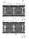
With reference now to FIG. 1a), and starting at a step [1100] of the method, a conductor sheet 150 is initially provided. The conductor sheet is preferably selected amongst a group of metal sheet materials comprising Cu, Cu/Ni, Ni/Fe, Cu plated Fe, Cu plated RVS (stainless steel), tin plated Fe, and metal plated polymers. The conductor sheet 150 is here a 200 μm thick copper sheet.
A first predetermined pattern 115 is at a step [1101] applied to the conductor sheet 150, thereby forming a first conductor structure 100, which corresponds to a specific mechanical and electronic layout while still maintaining the necessary integrity. The step of providing the first predetermined pattern is here done by means of laser cutting. Optionally, the first predetermined pattern 115 in the conductor sheet 100 is provided by means of a punching, or a masking and etching process. The first predetermined pattern 115 is selected to provide a plurality of component areas 111 dedicated for electrical and mechanical connection of LEDs 120. Each component area 111, comprises a pair of connection pads 111a, 111b separated by a gap A. The component areas 115 are further interconnected via meandering connection tracks 116 which are designed to, when stretched, form an electrical circuitry for a LED matrix.
For a typical LED matrix, a series parallel configuration of the electrical circuitry is provided, which is advantageous for being forgiving for LED failures. That is, failures arising from an open circuit or short circuit in the electrical circuitry of the LED matrix will only affect one row in the array, and a lighting application in which the LED matrix is integrated will still be functional. The connection tracks are here based on leads with a cross section of 0.2*0.2 mm and the length of the connection tracks are selected such that the finished LED matrix has a LED pitch of 75 mm in each dimension. The LED pitch for the LED matrix layout is preferably selected within a range of 50 to 100 mm, and the cross section of the connection tracks are selected depending on the material used in the conductor sheet.
As illustrated in FIGS. 1a) and 1b), the first predetermined pattern 115 is selected such that integrity of the conductor sheet 150 is governed by bridging portions 117. The first predetermined pattern 115 is here further selected for providing alignment holes 118 arranged in edge portions 125 of the conductor sheet 150 for alignment of the conductor sheet 150 in the mounting and trimming facilities during the mounting of LEDs, and stretch alignment holes 119 for applying a stretching tool, which will be described with reference to steps [1102] and [1104] respectively, herein under.
With reference now to FIG. 1b), in step [1102], the LEDs are mounted to the first conductor structure 100 forming a subassembly. The mounting may be done by means of a standard LED assembly process, i.e. solder is screen printed onto component areas connection pads 111a, 111b, and LEDs 120 are placed onto the component areas 111 followed by soldering of the LEDs 120, which soldering may be performed in a reflow soldering process.
In a step [1103] a final predetermined pattern corresponding to a second conductor structure 100′, i.e. the electronic circuitry of the LEDs 120, is provided to the subassembly by trimming of the bridging portions 117. The second conductor structure 100′ with the bridging portions 117 removed is illustrated in FIG. 1c). Further, the edge portions 125 of the conductor sheet 150 are trimmed off from the conductor circuitry. Trimming of the conductor sheet may be performed by e.g. laser cutting or punching. In a process of providing a number of subassemblies on a continuous conductor sheet, e.g. when the method is implemented in a reel-to-reel process, the processed conductor sheet is divided into a number of individual subassemblies (conductor structure with mounted LEDs).
Referring now to FIG. id), in step [1104] the subassembly, i.e. the conductor structure 100′ containing the trimmed meandering connection tracks 116 which electrically connects the LEDs 120, is stretched, thereby straightening the connection tracks 116. The stretching is performed in two dimensions such that the lead frame is expanded in two dimensions (x, y) to a final LED matrix. The maximum stretching force is preferably selected to be a factor 10 lower than the break force of the connection tracks, which depends on the selected conductor sheet material and the selected cross section of the connection tracks.
In the exemplifying embodiment, a 200 μm thick etched copper sheet provided with 13×13 LEDs interconnected with meandering (or folded) conductor portions is stretched and thereby expanded from an initial lead frame size of 30*200 mm to 600*600 mm. The area of the final LED matrix is thereby 60 times larger than the working size during manufacturing of the lead frame. Thus, the application of solder by screen printing, and mounting of components on the lead frame with meandering conductor portions, before stretching offers a very efficient, highly advantageous manufacturing method for large area LED matrices.
In FIG. 1e) the final LED array, i.e. the stretched subassembly 100″ is mounted on a substrate 200, which here is a tile, thereby forming a light tile 300. The final LED array may be arranged on any suitable substrate, for instance a reflector or an insulated heat sink. Light tiles according to the present inventions, as illustrated in FIG. 1e), are preferably manufactured with dimensions ranging from 600*600 to 600*1200 mm. Further, other applications like for instance head light applications are applicable for the present inventive concept, e.g. for TL retrofit in which dimensions of 150*150 mm are preferred.
According to an embodiment of the invention, the first predetermined pattern is selected such that thermal pads are integrated in the conductor structure. The thermal pads may be arranged at a component area, as illustrated in FIGS. 2a) and 2b). In FIG. 2a) a design for extra thermal pads 211 arranged at the component area 111 is shown, in which the thermal pad design is adapted for low power LEDs 120. For high power LEDs 220, larger thermal pads 212 are arranged at the component area 111 for facilitating thermal dissipation from the LEDs 220, as visualized in FIG. 2b).
According to an embodiment of the invention, referring now to FIG. 3, for mounting of small package LEDs 320, the component area 111 of the conductor structure is provided with a recess 311. As illustrated in the sequence performed in FIGS. 3a)-3d), here thermal pads 212 of the conductor structure (only a detail of the conductor structure is shown) are arranged at the component area 111, which comprises two dedicated connection pads 111a, 111b arranged having an initial gap A. The gap A is then reduced by means of forging tool 400, as illustrated in FIG. 3b). At the same time as the gap A is reduced, the forging tool 400 forms a recess 311 in the component area 111. The size of the recess 311 is selected to fit a small package component 320, and is here selected to fit a 0.5*0.5*0.3 mm Wafer Level Chip Scale Package, WLCSP. This step is advantageously integrated in a reel-to-reel process as described above.
The invention has mainly been described above with reference to a few embodiments. However, as is readily appreciated by a person skilled in the art, other embodiments than the ones disclosed above are equally possible within the scope of the invention, as defined by the appended claims.
Claims
1. A method for manufacturing an LED matrix comprising:
providing a first conductor structure comprising a plurality of component areas interconnected with meandering connection tracks by providing a conductor sheet with a first predetermined pattern;
mounting a plurality of LEDs to a respective component area of said first conductor structure thereby forming a subassembly;
trimming said subassembly to provide a second conductor structure; and
stretching said subassembly thereby straightening said connection tracks;
wherein said second conductor structure is arranged such that an m×n LED conductor matrix is formed during said step of stretching.
2. A method according to claim 1, further comprising:
arranging said stretched subassembly onto a substrate.
3. A method according to claim 1, wherein said first predetermined pattern is selected for providing at least one thermal pad area in said first or second conductor structure.
4. A method according to claim 3, wherein said at least one thermal pad area is arranged at a component area, or at a connection track.
5. A method according to claim 4, further comprising providing at least one recess in said component area for receiving LEDs or LED packages of a size less then 1×1×1 mm.
6. A method according to claim 5, wherein said step of mounting comprises:
defining solder areas on said first conductor structure;
applying solder onto said solder areas;
placing said LEDs on a respective component area, and performing soldering.
7. A method according to claim 6, wherein said first or second conductor structure is arranged with alignment features and/or stretch alignment features.
8. A method according to claim 7, further comprising providing mechanical deformation of said subassembly by means of one of splitting, trimming of the subassembly to a predetermined contour.
9. A method according to claim 8, further comprising deforming at least one portion of said subassembly to provide a predetermined lighting direction of at least one LED.
10. A method according to claim 9, further comprising providing deformation of said subassembly for providing one of: optical properties, mechanical fixation of said component interconnect board, mechanical fixation of additional components, thermal properties, and connector functionality.
11. A method according to claim 10, wherein at least one of providing said first predetermined pattern and said second conductor structure is done by means of etching, cutting, punching, slitting or laser cutting.
12. An LED matrix produced with a method according to claim 11.
13. A large area lighting device comprising the LED matrix according to claim 12.
Images & Drawings included:


Sources:
- United States Patent and Trademark Office - verify current appl. status at the USPTO↗
Similar patent applications:
Recent applications in this class:
- » 20250063877 2025-02-20
LED DISPLAY PANEL AND LED DISPLAY APPARATUS HAVING THE SAME - » 20240395851 2024-11-28
CHIP OF LED AND MANUFACTURING METHOD THEREOF - » 20240363673 2024-10-31
LED PACKAGE SET AND LED BULB INCLUDING SAME - » 20240055467 2024-02-15
Light emitting stacked structure including epitaxial layers connecting with electrodes and display device having the same - » 20230369381 2023-11-16
Display device, display module, electronic device, and manufacturing method of display device - » 20230299118 2023-09-21
LED STRUCTURE AND PREPARING METHOD OF LED STRUCTURE - » 20230238419 2023-07-27
ULTRAVIOLET LIGHT-EMITTING DEVICE - » 20230163155 2023-05-25
FAN-OUT LIGHT-EMITTING DIODE (LED) DEVICE SUBSTRATE WITH EMBEDDED BACKPLANE, LIGHTING SYSTEM AND METHOD OF MANUFACTURE - » 20230005984 2023-01-05
Light-emitting device and manufacturing method thereof - » 20220336523 2022-10-20
SEMICONDUCTOR DEVICE AND DISPLAY DEVICE
Recent applications for this Assignee:
- » 20250255572 2025-08-14
AUTO POSITIONING OF X-RAY TUBE SUPPORT WITH RESPECT TO DETECTOR - » 20250174211 2025-05-29
MIXING SECONDARY GRAPHICS ELEMENTS IN HDR IMAGES - » 20250068867 2025-02-27
MULTIPLE APPLICATION QR CODE - » 20250061555 2025-02-20
APPARATUS AND METHOD FOR DYNAMIC RANGE TRANSFORMING OF IMAGES - » 20250061554 2025-02-20
APPARATUS AND METHOD FOR DYNAMIC RANGE TRANSFORMING OF IMAGES - » 20240422887 2024-12-19
DYNAMIC IMAGING SYSTEM WORKFLOW OPTIMIZATION - » 20240420325 2024-12-19
Network architecture for 3D image processing - » 20240415487 2024-12-19
A FETAL MOVEMENT DETECTION METHOD FROM DOPPLER ULTRASOUND SIGNAL - » 20240381324 2024-11-14
COMMUNICATION DEVICE, SYSTEM AND METHOD FOR COMMUNICATION USING FEEBACK - » 20240349283 2024-10-17
Hybrid automatic repeat request feedback in radio systems