TFET with nanowire source
US20140239258A1
2014-08-28
13/571,657
2012-08-10
✅ Patent granted
US 8,946,680 B2
2015-02-03
-
-
Edward Wojciechowicz
Cantor Colburn LLP | Vazken Alexanian
2033-02-22
Abstract:
A tunnel field effect transistor (TFET) includes a source region, the source region comprising a first portion of a nanowire; a channel region, the channel region comprising a second portion of the nanowire; a drain region, the drain region comprising a portion of a silicon pad, the silicon pad being located adjacent to the channel region; and a gate configured such that the gate surrounds the channel region and at least a portion of the source region.
Inventors:
- Sarunya Bangsaruntip 63 🇺🇸 Mount Kisco, NY, United States
- Isaac Lauer 35 🇺🇸 Mahopac, NY, United States
- Amlan Majumdar 116 🇺🇸 White Plains, NY, United States
- Jeffrey Sleight 1 🇺🇸 Ridgefield, NY, United States
Assignee:
- INTERNATIONAL BUSINESS MACHINES CORPORATION 136,239 🇺🇸 ARMONK, NY, United States
Applicant:
Interested in similar patents?
Get notified when new applications in this technology area are published.
Classification:
H01L29/0895 » CPC further
Semiconductor devices adapted for rectifying, amplifying, oscillating or switching, or capacitors or resistors with at least one potential-jump barrier or surface barrier, e.g. PN junction depletion layer or carrier concentration layer; Details of semiconductor bodies or of electrodes thereof; Multistep manufacturing processes therefor; Semiconductor bodies ; Multistep manufacturing processes therefor characterised by their shape; characterised by the shapes, relative sizes, or dispositions of the semiconductor regions ; characterised by the concentration or distribution of impurities within semiconductor regions with semiconductor regions connected to an electrode carrying current to be rectified, amplified or switched and such electrode being part of a semiconductor device which comprises three or more electrodes Tunnel injectors
H01L29/0847 » CPC main
Semiconductor devices adapted for rectifying, amplifying, oscillating or switching, or capacitors or resistors with at least one potential-jump barrier or surface barrier, e.g. PN junction depletion layer or carrier concentration layer; Details of semiconductor bodies or of electrodes thereof; Multistep manufacturing processes therefor; Semiconductor bodies ; Multistep manufacturing processes therefor characterised by their shape; characterised by the shapes, relative sizes, or dispositions of the semiconductor regions ; characterised by the concentration or distribution of impurities within semiconductor regions with semiconductor regions connected to an electrode carrying current to be rectified, amplified or switched and such electrode being part of a semiconductor device which comprises three or more electrodes; Source or drain regions of field-effect devices of field-effect transistors with insulated gate
H01L29/0669 » CPC main
Semiconductor devices adapted for rectifying, amplifying, oscillating or switching, or capacitors or resistors with at least one potential-jump barrier or surface barrier, e.g. PN junction depletion layer or carrier concentration layer; Details of semiconductor bodies or of electrodes thereof; Multistep manufacturing processes therefor; Semiconductor bodies ; Multistep manufacturing processes therefor characterised by their shape; characterised by the shapes, relative sizes, or dispositions of the semiconductor regions ; characterised by the concentration or distribution of impurities within semiconductor regions characterised by the shape of the body the shape of the body defining a nanostructure Nanowires or nanotubes
H01L29/0665 » CPC further
Semiconductor devices adapted for rectifying, amplifying, oscillating or switching, or capacitors or resistors with at least one potential-jump barrier or surface barrier, e.g. PN junction depletion layer or carrier concentration layer; Details of semiconductor bodies or of electrodes thereof; Multistep manufacturing processes therefor; Semiconductor bodies ; Multistep manufacturing processes therefor characterised by their shape; characterised by the shapes, relative sizes, or dispositions of the semiconductor regions ; characterised by the concentration or distribution of impurities within semiconductor regions characterised by the shape of the body the shape of the body defining a nanostructure
H01L29/0673 » CPC further
Semiconductor devices adapted for rectifying, amplifying, oscillating or switching, or capacitors or resistors with at least one potential-jump barrier or surface barrier, e.g. PN junction depletion layer or carrier concentration layer; Details of semiconductor bodies or of electrodes thereof; Multistep manufacturing processes therefor; Semiconductor bodies ; Multistep manufacturing processes therefor characterised by their shape; characterised by the shapes, relative sizes, or dispositions of the semiconductor regions ; characterised by the concentration or distribution of impurities within semiconductor regions characterised by the shape of the body the shape of the body defining a nanostructure; Nanowires or nanotubes oriented parallel to a substrate
H01L29/66477 » CPC further
Semiconductor devices adapted for rectifying, amplifying, oscillating or switching, or capacitors or resistors with at least one potential-jump barrier or surface barrier, e.g. PN junction depletion layer or carrier concentration layer; Details of semiconductor bodies or of electrodes thereof; Multistep manufacturing processes therefor; Types of semiconductor device ; Multistep manufacturing processes therefor; Multistep manufacturing processes of devices having semiconductor bodies comprising group 14 or group 13/15 materials the devices being controllable only by the electric current supplied or the electric potential applied, to an electrode which does not carry the current to be rectified, amplified or switched, e.g. three-terminal devices; Unipolar field-effect transistors with an insulated gate, i.e. MISFET
H01L29/66977 » CPC further
Semiconductor devices adapted for rectifying, amplifying, oscillating or switching, or capacitors or resistors with at least one potential-jump barrier or surface barrier, e.g. PN junction depletion layer or carrier concentration layer; Details of semiconductor bodies or of electrodes thereof; Multistep manufacturing processes therefor; Types of semiconductor device ; Multistep manufacturing processes therefor Quantum effect devices, e.g. using quantum reflection, diffraction or interference effects, i.e. Bragg- or Aharonov-Bohm effects
H01L29/7391 » CPC further
Semiconductor devices adapted for rectifying, amplifying, oscillating or switching, or capacitors or resistors with at least one potential-jump barrier or surface barrier, e.g. PN junction depletion layer or carrier concentration layer; Details of semiconductor bodies or of electrodes thereof; Multistep manufacturing processes therefor; Types of semiconductor device ; Multistep manufacturing processes therefor controllable by only the electric current supplied, or only the electric potential applied, to an electrode which does not carry the current to be rectified, amplified or switched; Bipolar devices; Transistor-type devices, i.e. able to continuously respond to applied control signals controlled by field-effect, e.g. bipolar static induction transistors [BSIT] Gated diode structures
H01L29/402 » CPC further
Semiconductor devices adapted for rectifying, amplifying, oscillating or switching, or capacitors or resistors with at least one potential-jump barrier or surface barrier, e.g. PN junction depletion layer or carrier concentration layer; Details of semiconductor bodies or of electrodes thereof; Multistep manufacturing processes therefor; Electrodes ; Multistep manufacturing processes therefor Field plates
Y10S977/723 » CPC further
Nanotechnology; Nanostructure; Integrated with dissimilar structures on a common substrate On an electrically insulating substrate
Y10S977/938 » CPC further
Nanotechnology; Specified use of nanostructure for electronic or optoelectronic application in a transistor or 3-terminal device Field effect transistors, FETS, with nanowire- or nanotube-channel region
H01L29/72 IPC
Semiconductor devices adapted for rectifying, amplifying, oscillating or switching, or capacitors or resistors with at least one potential-jump barrier or surface barrier, e.g. PN junction depletion layer or carrier concentration layer; Details of semiconductor bodies or of electrodes thereof; Multistep manufacturing processes therefor; Types of semiconductor device ; Multistep manufacturing processes therefor controllable by only the electric current supplied, or only the electric potential applied, to an electrode which does not carry the current to be rectified, amplified or switched; Bipolar devices Transistor-type devices, i.e. able to continuously respond to applied control signals
H01L29/08 IPC
Semiconductor devices adapted for rectifying, amplifying, oscillating or switching, or capacitors or resistors with at least one potential-jump barrier or surface barrier, e.g. PN junction depletion layer or carrier concentration layer; Details of semiconductor bodies or of electrodes thereof; Multistep manufacturing processes therefor; Semiconductor bodies ; Multistep manufacturing processes therefor characterised by their shape; characterised by the shapes, relative sizes, or dispositions of the semiconductor regions ; characterised by the concentration or distribution of impurities within semiconductor regions with semiconductor regions connected to an electrode carrying current to be rectified, amplified or switched and such electrode being part of a semiconductor device which comprises three or more electrodes
H01L29/786 IPC
Semiconductor devices adapted for rectifying, amplifying, oscillating or switching, or capacitors or resistors with at least one potential-jump barrier or surface barrier, e.g. PN junction depletion layer or carrier concentration layer; Details of semiconductor bodies or of electrodes thereof; Multistep manufacturing processes therefor; Types of semiconductor device ; Multistep manufacturing processes therefor controllable by only the electric current supplied, or only the electric potential applied, to an electrode which does not carry the current to be rectified, amplified or switched; Unipolar devices, e.g. field effect transistors; Field effect transistors with field effect produced by an insulated gate Thin film transistors, i.e. transistors with a channel being at least partly a thin film
H01L29/40 IPC
Semiconductor devices adapted for rectifying, amplifying, oscillating or switching, or capacitors or resistors with at least one potential-jump barrier or surface barrier, e.g. PN junction depletion layer or carrier concentration layer; Details of semiconductor bodies or of electrodes thereof; Multistep manufacturing processes therefor Electrodes ; Multistep manufacturing processes therefor
H01L29/06 IPC
Semiconductor devices adapted for rectifying, amplifying, oscillating or switching, or capacitors or resistors with at least one potential-jump barrier or surface barrier, e.g. PN junction depletion layer or carrier concentration layer; Details of semiconductor bodies or of electrodes thereof; Multistep manufacturing processes therefor; Semiconductor bodies ; Multistep manufacturing processes therefor characterised by their shape; characterised by the shapes, relative sizes, or dispositions of the semiconductor regions ; characterised by the concentration or distribution of impurities within semiconductor regions
B82Y10/00 » CPC further
Nanotechnology for information processing, storage or transmission, e.g. quantum computing or single electron logic
H01L29/423 IPC
Semiconductor devices adapted for rectifying, amplifying, oscillating or switching, or capacitors or resistors with at least one potential-jump barrier or surface barrier, e.g. PN junction depletion layer or carrier concentration layer; Details of semiconductor bodies or of electrodes thereof; Multistep manufacturing processes therefor; Electrodes ; Multistep manufacturing processes therefor characterised by their shape, relative sizes or dispositions not carrying the current to be rectified, amplified or switched
H01L29/66 IPC
Semiconductor devices adapted for rectifying, amplifying, oscillating or switching, or capacitors or resistors with at least one potential-jump barrier or surface barrier, e.g. PN junction depletion layer or carrier concentration layer; Details of semiconductor bodies or of electrodes thereof; Multistep manufacturing processes therefor Types of semiconductor device ; Multistep manufacturing processes therefor
H01L29/775 » CPC further
Semiconductor devices adapted for rectifying, amplifying, oscillating or switching, or capacitors or resistors with at least one potential-jump barrier or surface barrier, e.g. PN junction depletion layer or carrier concentration layer; Details of semiconductor bodies or of electrodes thereof; Multistep manufacturing processes therefor; Types of semiconductor device ; Multistep manufacturing processes therefor controllable by only the electric current supplied, or only the electric potential applied, to an electrode which does not carry the current to be rectified, amplified or switched; Unipolar devices, e.g. field effect transistors; Field effect transistors with one dimensional charge carrier gas channel, e.g. quantum wire FET
H01L29/739 IPC
Semiconductor devices adapted for rectifying, amplifying, oscillating or switching, or capacitors or resistors with at least one potential-jump barrier or surface barrier, e.g. PN junction depletion layer or carrier concentration layer; Details of semiconductor bodies or of electrodes thereof; Multistep manufacturing processes therefor; Types of semiconductor device ; Multistep manufacturing processes therefor controllable by only the electric current supplied, or only the electric potential applied, to an electrode which does not carry the current to be rectified, amplified or switched; Bipolar devices; Transistor-type devices, i.e. able to continuously respond to applied control signals controlled by field-effect, e.g. bipolar static induction transistors [BSIT]
H01L29/78 » CPC further
Semiconductor devices adapted for rectifying, amplifying, oscillating or switching, or capacitors or resistors with at least one potential-jump barrier or surface barrier, e.g. PN junction depletion layer or carrier concentration layer; Details of semiconductor bodies or of electrodes thereof; Multistep manufacturing processes therefor; Types of semiconductor device ; Multistep manufacturing processes therefor controllable by only the electric current supplied, or only the electric potential applied, to an electrode which does not carry the current to be rectified, amplified or switched; Unipolar devices, e.g. field effect transistors; Field effect transistors with field effect produced by an insulated gate
Description
CROSS REFERENCE TO RELATED APPLICATION
This application is a divisional of U.S. application Ser. No. 12/777,881, filed on May 11, 2010 the disclosure of which are incorporated herein by reference in their entirety.
FEDERAL RESEARCH STATEMENT
This invention was made with Government support under Government Contract FA8650-08-C-7806, awarded by the Defense Advanced Research Projects Agency (DARPA). The Government has certain rights in this invention.
FIELD
This disclosure relates generally to the field of tunnel field effect transistors.
DESCRIPTION OF RELATED ART
Tunnel field effect transistors (TFETs) may be used as a replacement for or complement to metal-oxide-semiconductor FETs (MOSFETs). A TFET may comprise a nanowire channel, which may provide good electrostatic control of the channel due to gate-all-around (GAA) geometry. However, relatively high fields at the drain end of a nanowire channel TFET may lead to parasitic ambipolar behavior that increases the TFET off current, resulting in a relatively inefficient device.
SUMMARY
In one aspect, a tunnel field effect transistor (TFET) includes a source region, the source region comprising a first portion of a nanowire; a channel region, the channel region comprising a second portion of the nanowire; a drain region, the drain region comprising a portion of a silicon pad, the silicon pad being located adjacent to the channel region; and a gate configured such that the gate surrounds the channel region and at least a portion of the source region.
Additional features are realized through the techniques of the present exemplary embodiment. Other embodiments are described in detail herein and are considered a part of what is claimed. For a better understanding of the features of the exemplary embodiment, refer to the description and to the drawings.
BRIEF DESCRIPTION OF THE SEVERAL VIEWS OF THE DRAWINGS
Referring now to the drawings wherein like elements are numbered alike in the several FIGURES:
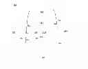
FIG. 1 illustrates an embodiment of a method of forming a TFET with a nanowire source.
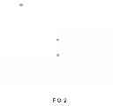
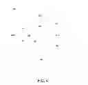
FIG. 2 illustrates an embodiment of a silicon-on-insulator (SOI) wafer.
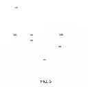
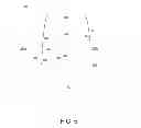
FIG. 3 illustrates an embodiment of the SOI wafer of FIG. 2 after formation of a nanowire.
FIG. 4 illustrates an embodiment of the structure of FIG. 3 after formation of a gate.
FIG. 5 illustrates an embodiment of the structure of FIG. 4 after formation of a spacer.
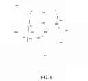
FIG. 6 illustrates an embodiment of the structure of FIG. 5 after formation of the drain region.
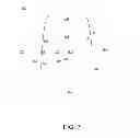
FIG. 7 illustrates an embodiment of a TFET with a nanowire source.
DETAILED DESCRIPTION
Embodiments of systems and methods for a TFET with a nanowire source are provided, with exemplary embodiments being discussed below in detail. The TFET source injection point may be located in a GAA nanowire, and the drain may be located in a planar single-gated region. This configuration suppresses ambipolar behavior in the TFET, thereby reducing the TFET off current.
FIG. 1 illustrates an embodiment of a method of forming a TFET with a nanowire source. FIG. 1 is discussed with reference to FIGS. 2-7. In block 101, a SOI wafer 200 as shown in FIG. 2 is used to form a structure 300 comprising a silicon nanowire 302 as shown in FIG. 3. SOI wafer 200 comprises silicon substrate 201 under buried oxide (BOX) 202 under silicon layer 203. To form nanowire 302, the locations of nanowire 302 and silicon pads 301A-B are lithographically defined and etched in silicon layer 203. After nanowire 302 and silicon pads 301A-B are etched, a portion of BOX 202 is removed to form recess 303 under nanowire 302 and silicon pads 301A-B. Recess 303 may be formed using a hydrofluoric (HF) acid dip in some embodiments. Nanowire 302 is located between silicon pads 301A-B, may have a length between about 50 nanometers (nm) and about 200 nm in some embodiments, and may have a diameter between about 3 nm and about 50 nm in some embodiments.
In block 102, a gate comprising dielectric layer 401 and gate polysilicon 402 is formed around nanowire 302 and in recess 303, as shown in FIG. 4. The gate has a GAA configuration. Dielectric layer 401 completely surrounds nanowire 302. Dielectric layer 401 may comprise thermally grown oxide or a high-k material in some embodiments. The gate may optionally comprise a metal layer (not shown) located between dielectric layer 401 and gate polysilicon 402. A hardmask layer 403, which may comprise silicon nitride, is then formed over the gate polysilicon 402.
In block 103, a spacer 501 is formed adjacent to the gate comprising dielectric layer 401 and gate polysilicon 402, as shown in FIG. 5. Spacer 501 may comprise a nitride in some embodiments.
In block 104, a drain region 601 is formed in silicon pad 301B by implantation of dopants, as shown in FIG. 6. Drain region 601 may be implanted with n-type dopants including but not limited to arsenic (As) or phosphorous (P). Implantation of drain region 601 may be followed by an anneal in some embodiments. Drain region 601 is located in a planar single-gated region
In block 105, silicon pad 301A and a portion of nanowire 302 are implanted with dopants to form nanowire source 701 as shown in FIG. 7. Nanowire source 701 may be implanted with p-type dopants including but not limited to boron (B) or boron diflouride (BF2). Implantation of nanowire source 701 is followed by an anneal. The resulting device comprises a TFET 700 with a nanowire source 701. A portion of nanowire source 701 comprises a GAA configuration (i.e., a portion of nanowire source 701 is located inside the gate of TFET 700). The undoped portion of nanowire 302 comprises the channel of TFET 700; the channel also comprises a GAA configuration. TFET 700 may exhibit good electrostatic control of the nanowire channel 302 while having reduced ambipolar behavior due to the GAA portion of nanowire source 701. In some embodiments, hardmask layer 403 may be removed after formation of nanowire source 701, and a top portion of gate polysilicon 402 may be silicided to form a gate contact (not shown).
The technical effects and benefits of exemplary embodiments include formation of a TFET with reduced off current.
The terminology used herein is for the purpose of describing particular embodiments only and is not intended to be limiting of the invention. As used herein, the singular forms “a”, “an”, and “the” are intended to include the plural forms as well, unless the context clearly indicates otherwise. It will be further understood that the terms “comprises” and/or “comprising,” when used in this specification, specify the presence of stated features, integers, steps, operations, elements, and/or components, but do not preclude the presence or addition of one or more other features, integers, steps, operations, elements, components, and/or groups thereof.
The corresponding structures, materials, acts, and equivalents of all means or step plus function elements in the claims below are intended to include any structure, material, or act for performing the function in combination with other claimed elements as specifically claimed. The description of the present invention has been presented for purposes of illustration and description, but is not intended to be exhaustive or limited to the invention in the form disclosed. Many modifications and variations will be apparent to those of ordinary skill in the art without departing from the scope and spirit of the invention. The embodiment was chosen and described in order to best explain the principles of the invention and the practical application, and to enable others of ordinary skill in the art to understand the invention for various embodiments with various modifications as are suited to the particular use contemplated.
Claims
1. A tunnel field effect transistor (TFET), comprising:
a source region, the source region comprising a first portion of a nanowire;
a channel region, the channel region comprising a second portion of the nanowire;
a drain region, the drain region comprising a portion of a silicon pad, the silicon pad being located adjacent to the channel region; and
a gate configured such that the gate surrounds the channel region and at least a portion of the source region.
2. The TFET of claim 1, wherein the nanowire comprises silicon, and the source region further comprises a silicon pad located adjacent to the first portion of the nanowire.
3. The TFET of claim 1, wherein the source region is doped with p-type dopants, and the drain region is doped with n-type dopants.
4. The TFET of claim 1, wherein the gate comprises a dielectric layer and a gate polysilicon region, wherein the dielectric layer is located adjacent to and surrounding the nanowire, and the gate polysilicon region is located over the dielectric layer.
5. The TFET of claim 4, wherein the dielectric layer is formed adjacent to and surrounding a first portion of the nanowire and a first portion of the second silicon pad, the gate polysilicon region is formed over the dielectric layer, and wherein the gate is located on top of the first portion of the second silicon pad, and is not located on top of any portion of the first silicon pad.
6. The TFET of claim 5, wherein the drain region is located in a second portion of the second silicon pad that is not located underneath the gate.
7. The TFET of claim 5, wherein the source is located in the first silicon pad and a second portion of the nanowire.
8. The TFET of claim 4, wherein the gate further comprises a metal layer located between the dielectric layer and the gate polysilicon region.
9. The TFET of claim 4, wherein the dielectric layer comprises one of thermally grown oxide and a high-k material.
10. The TFET of claim 1, further comprising a spacer comprising a nitride located adjacent to the gate.
Images & Drawings included:
Sources:
- United States Patent and Trademark Office - verify current appl. status at the USPTO↗
Similar patent applications:
- » 20110278542
TFET with nanowire source
Recent applications in this class:
- » 20250072070 2025-02-27
SEMICONDUCTOR DEVICES AND METHODS OF FABRICATING THE SAME - » 20250072069 2025-02-27
RECESSED VIA WITH CONDUCTIVE LINK TO ADJACENT CONTACT - » 20250063783 2025-02-20
CONTACT STRUCTURE FOR SEMICONDUCTOR DEVICE AND METHOD - » 20250063782 2025-02-20
INTEGRATED CIRCUIT DEVICE INCLUDING WIMPY TRANSISTOR STACK WITH THICK SOURCE/DRAIN ISOLATION LAYER AND METHODS OF FORMING TING THE SAME - » 20250056852 2025-02-13
SOURCE/DRAIN REGIONS IN COMPLEMENTARY FIELD EFFECT TRANSISTORS AND METHODS OF FORMING THE SAME - » 20250048698 2025-02-06
GATE-ALL-AROUND INTEGRATED CIRCUIT STRUCTURES HAVING SOURCE OR DRAIN STRUCTURES WITH EPITAXIAL NUBS - » 20250048697 2025-02-06
SEMICONDUCTOR DEVICES INCLUDING GATE STRUCTURES AND IMPURITY REGIONS - » 20250048696 2025-02-06
SEMICONDUCTOR DEVICE AND METHOD OF FABRICATING THE SAME - » 20250048695 2025-02-06
MULTI-GATE FET WITH SELF-ALIGNED TAPERED ACTIVE REGION EDGE - » 20250048694 2025-02-06
SEMICONDUCTOR DEVICE STRUCTURE AND METHODS OF FORMING THE SAME
Recent applications for this Assignee:
- » 20250294045 2025-09-18
THREAT POLICY FINE-TUNING BASED ON THE VULNERABILITY OF A SUBNET AS A SOURCE OF A MALICIOUS ATTACK - » 20250294041 2025-09-18
DEVICE POPULATION ANOMALY DETECTION - » 20250292574 2025-09-18
SCENE PARSING - » 20250292026 2025-09-18
A GENERATIVE ARTIFICIAL INTELLIGENCE COMMENTARY - » 20250291689 2025-09-18
MACHINE LEARNING MODEL TRAINING TO ASSIST IN SYSTEM DEBUG - » 20250287215 2025-09-11
PORTABLE MEDIA GEOFENCE AND DEVICE PAIRING SECURITY - » 20250285610 2025-09-11
RECIPIENT-SPECIFIC VOICE TONE ADJUSTMENT IN TELEPHONY - » 20250284728 2025-09-11
CONTEXT LARGE LANGUAGE MODEL OUTPUT EXPLANATION - » 20250278669 2025-09-04
COUNTERFACTUALS WITH FEATURE PREFERENCES FOR CONSISTENT AND DIVERSE EXPLANATIONS - » 20250274345 2025-08-28
MULTI-LAYER EDGE ARCHITECTURE SIMULATION