Depletion-mode field-effect transistor-based phototransistor
US20140363917A1
2014-12-11
14/461,038
2014-08-15
✅ Patent granted
US 9,343,608 B2
2016-05-17
-
-
Long Pham
Antony P. Ng | Russell Ng PLLC
2034-08-15
Abstract:
A depletion-mode phototransitor is disclosed. The phototransistor having a substrate, a gate, a source, a drain and a channel. The source, drain and channel are doped to be the same type of semiconductor. The substrate can be made of silicon and/or germanium. The gate can be made of either aluminum or polysilicon.
Inventors:
- Krishna C. Saraswat 10 🇺🇸 Saratoga, CA, United States
- YEUL NA 5 🇺🇸 Santa Clara, CA, United States
Assignee:
- Board of Regents, The University of Texas System 3,219 🇺🇸 Austin, TX, United States
- The Board of Trustees of the Leland Stanford Junior University 2,156 🇺🇸 Stanford, CA, United States
Applicant:
Interested in similar patents?
Get notified when new applications in this technology area are published.
Classification:
H01L31/18 » CPC further
Semiconductor devices sensitive to infra-red radiation, light, electromagnetic radiation of shorter wavelength or corpuscular radiation and specially adapted either for the conversion of the energy of such radiation into electrical energy or for the control of electrical energy by such radiation; Processes or apparatus specially adapted for the manufacture or treatment thereof or of parts thereof; Details thereof Processes or apparatus specially adapted for the manufacture or treatment of these devices or of parts thereof
H01L31/1129 » CPC main
Semiconductor devices sensitive to infra-red radiation, light, electromagnetic radiation of shorter wavelength or corpuscular radiation and specially adapted either for the conversion of the energy of such radiation into electrical energy or for the control of electrical energy by such radiation; Processes or apparatus specially adapted for the manufacture or treatment thereof or of parts thereof; Details thereof in which radiation controls flow of current through the device, e.g. photoresistors characterised by at least one potential-jump barrier or surface barrier, e.g. phototransistors; Devices sensitive to infra-red, visible or ultra-violet radiation characterised by field-effect operation, e.g. junction field-effect phototransistor; Devices with PN heterojunction gate the device being a field-effect phototransistor
H01L27/14612 » CPC further
Devices consisting of a plurality of semiconductor or other solid-state components formed in or on a common substrate including semiconductor components sensitive to infra-red radiation, light, electromagnetic radiation of shorter wavelength or corpuscular radiation and specially adapted either for the conversion of the energy of such radiation into electrical energy or for the control of electrical energy by such radiation; Devices controlled by radiation; Imager structures; Structural or functional details thereof; Pixel-elements with integrated switching, control, storage or amplification elements involving a transistor
H01L31/1136 » CPC further
Semiconductor devices sensitive to infra-red radiation, light, electromagnetic radiation of shorter wavelength or corpuscular radiation and specially adapted either for the conversion of the energy of such radiation into electrical energy or for the control of electrical energy by such radiation; Processes or apparatus specially adapted for the manufacture or treatment thereof or of parts thereof; Details thereof in which radiation controls flow of current through the device, e.g. photoresistors characterised by at least one potential-jump barrier or surface barrier, e.g. phototransistors; Devices sensitive to infra-red, visible or ultra-violet radiation characterised by field-effect operation, e.g. junction field-effect phototransistor being of the conductor-insulator-semiconductor type, e.g. metal-insulator-semiconductor field-effect transistor the device being a metal-insulator-semiconductor field-effect transistor
Y02E10/50 » CPC further
Energy generation through renewable energy sources Photovoltaic [PV] energy
Y02E10/50 » CPC further
Energy generation through renewable energy sources Photovoltaic [PV] energy
H01L31/062 » CPC further
Semiconductor devices sensitive to infra-red radiation, light, electromagnetic radiation of shorter wavelength or corpuscular radiation and specially adapted either for the conversion of the energy of such radiation into electrical energy or for the control of electrical energy by such radiation; Processes or apparatus specially adapted for the manufacture or treatment thereof or of parts thereof; Details thereof adapted as photovoltaic [PV] conversion devices characterised by at least one potential-jump barrier or surface barrier the potential barriers being only of the metal-insulator-semiconductor type
H01L27/14689 » CPC further
Devices consisting of a plurality of semiconductor or other solid-state components formed in or on a common substrate including semiconductor components sensitive to infra-red radiation, light, electromagnetic radiation of shorter wavelength or corpuscular radiation and specially adapted either for the conversion of the energy of such radiation into electrical energy or for the control of electrical energy by such radiation; Devices controlled by radiation; Imager structures; Processes or apparatus peculiar to the manufacture or treatment of these devices or parts thereof MOS based technologies
H01L31/112 IPC
Semiconductor devices sensitive to infra-red radiation, light, electromagnetic radiation of shorter wavelength or corpuscular radiation and specially adapted either for the conversion of the energy of such radiation into electrical energy or for the control of electrical energy by such radiation; Processes or apparatus specially adapted for the manufacture or treatment thereof or of parts thereof; Details thereof in which radiation controls flow of current through the device, e.g. photoresistors characterised by at least one potential-jump barrier or surface barrier, e.g. phototransistors; Devices sensitive to infra-red, visible or ultra-violet radiation characterised by field-effect operation, e.g. junction field-effect phototransistor
H01L27/146 IPC
Devices consisting of a plurality of semiconductor or other solid-state components formed in or on a common substrate including semiconductor components sensitive to infra-red radiation, light, electromagnetic radiation of shorter wavelength or corpuscular radiation and specially adapted either for the conversion of the energy of such radiation into electrical energy or for the control of electrical energy by such radiation; Devices controlled by radiation Imager structures
H01L31/113 IPC
Semiconductor devices sensitive to infra-red radiation, light, electromagnetic radiation of shorter wavelength or corpuscular radiation and specially adapted either for the conversion of the energy of such radiation into electrical energy or for the control of electrical energy by such radiation; Processes or apparatus specially adapted for the manufacture or treatment thereof or of parts thereof; Details thereof in which radiation controls flow of current through the device, e.g. photoresistors characterised by at least one potential-jump barrier or surface barrier, e.g. phototransistors; Devices sensitive to infra-red, visible or ultra-violet radiation characterised by field-effect operation, e.g. junction field-effect phototransistor being of the conductor-insulator-semiconductor type, e.g. metal-insulator-semiconductor field-effect transistor
Description
PRIORITY CLAIM
The present application is a continuation of U.S. patent application Ser. No. 13/835,662, filed on Mar. 15, 2013, the contents of which are incorporated herein by reference.
BACKGROUND OF THE INVENTION
1. Technical Field
The present invention relates to phototransistors in general, and in particular to a depletion-mode field-effect transistor-based phototransistor.
2. Description of Related Art
While the scaling down of dimensions of electronic devices has provided dramatic improvements in their performance, on-chip/off-chip interconnects have become a major performance bottleneck because the scaling also reduces cross-sectional dimensions. As a result, conventional schemes for metal interconnects become problematic in terms of latency, bandwidth and power.
The usage of optical interconnects can avoid the resistive loss and capacitive physics of metal interconnects. Optical interconnects can also help to meet the latency and bandwidth requirements. However, the energy per bit of the optical interconnects is still too high compared to that of their metal counterparts except for long wires. While some modulator schemes promise to satisfy power requirements for on-chip interconnects, lasers and receiver circuits still have technological problems. These problems are inherent in photodiodes that are commonly used as photodetectors in optical receiver circuits. Because of the diffraction limit of light, a photodiode is not scalable, and therefore a device with sub-wavelength dimensions suffers from reduced responsivity. In addition, photodiodes have a much larger footprints than many electronic devices, which may lead to large output capacitances, large dark currents, and high power consumption in receiver circuits.
In addition, typical photodiodes have a theoretical limit on the external quantum efficiency (EQE) of 1, or a responsivity of ˜0.7 A/W at 850 nm wavelength. This limitation and the large dark current require a high optical input signal in order to maintain a sufficient signal-to-noise ratio. Thus, optical emitters can consume a large amount of power. Even though previous studies on phototransistors have shown that they have a high responsivity, those devices suffered from increased dark current and a longer response time.
Rather than collecting generated electron-hole pairs directly, it is possible to use the carriers to change the band bending in the device, and thereby modulate the potential and thus the output current. Theoretically, this method has the potential to overcome theoretical limitation on EQE, but in practice, it has been impossible to demonstrate that the above-mentioned method has a better performance than that of is photodiodes. Furthermore, since these photodiodes are not scalable, large output capacitances are still problematic.
Consequently, it would be desirable to provide an improved phototransistor to be used in conjunction with optical interconnects.
SUMMARY OF THE INVENTION
In accordance with a preferred embodiment of the present invention, a phototransistor having a substrate, a gate, a source, a drain and a channel. The source, drain and channel are doped to be the same type of semiconductor. The substrate can be made of silicon and/or germanium. The gate can be made of either aluminum or polysilicon.
All features and advantages of the present invention will become apparent in the following detailed written description.
BRIEF DESCRIPTION OF THE DRAWINGS
The invention itself, as well as a preferred mode of use, further objects, and advantages thereof, will best be understood by reference to the following detailed description of an illustrative embodiment when read in conjunction with the accompanying drawings, wherein;
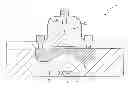
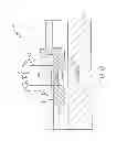
FIG. 1 is a diagram of a depletion-mode metal-oxide semiconductor field-effect transistor-based phototransistor, in accordance with a preferred embodiment of the present invention;
FIGS. 2a-2e illustrate the progression of changes in the band diagrams for the phototransistor from FIG. 1 upon illumination;
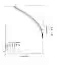
FIGS. 3a-3b are ID-VG curves for the phototransistor from FIG. 1 at various light intensities;
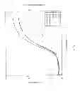
FIG. 4 shows the responsivity for the phototransistor from FIG. 1 at various light intensities;
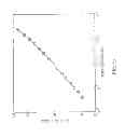
FIG. 5 depicts a plot of the gate voltage shift versus the intensity of an incident light; and
FIG. 6 shows a p-type germanium depletion-mode field-effect transistor-based phototransistor.
DETAILED DESCRIPTION OF A PREFERRED EMBODIMENT
Referring now to the drawings, and in particular to FIG. 1, there is depicted a diagram of a depletion-mode metal-oxide semiconductor field-effect transistor (MOSFET) based phototransistor, in accordance with a preferred embodiment of the present invention. As shown, a phototransistor 10 includes a floating substrate 11, a gate 12, a source 13, a drain 14 and a channel 15. Substrate 11 is preferably made of silicon. Gate 12 is preferably made of either aluminum or polysilicon. Source 13, drain 14 and channel 15 are doped to have the same type of semiconductor (e.g., n-type in FIG. 1) while substrate 11 is doped to have the opposite type of semiconductor (e.g., p-type in FIG. 1).
Phototransistor 10 can be fabricated as follows. Initially, a p-well is formed in an n-type silicon substrate (˜1e17 cm−3) (such as substrate 11 from FIG. 1) via an ion implantation with 1e14 cm−2 of boron at 50 keV. A source (such as source 13 from FIG. 1) and a drain (such as drain 14 from FIG. 1) are then formed by an ion implantation with 2e15 cm−2 of arsenic at 40 keV. Next, a channel (such as channel 15 from FIG. 1) is formed by an ion implantation with 2e13 cm−2 of arsenic at 10 keV. The ion implantation formed an n-type channel with a peak doping density of 2e19 cm−3 and a junction depth of 15 nm. Then, a layer of silicon dioxide (SiO2), e.g., 7 nm thick, is thermally grown on top of the substrate, followed by a deposition of aluminum, e.g., 200 nm thick, and a dry-etching to form a gate (such as gate 12 from FIG. 1). Another layer of low-temperature oxide, such as SiO2, can be deposited on the gate and the substrate in order to passivate the surface of the gate and substrate. Finally, a via etch and metallization are performed to make contacts for gate 12, source 13 and drain 14.
One main difference between phototransistor 10 and a conventional MOSFET is that channel 15 is doped to have the same type of semiconductor as source 13/drain 14. By doing so, the current is transported through an accumulation layer, not through a strong inversion layer (which is the characteristic of MOSFETs). Thus, substrate 11 and the interface between channel 15 and the gate dielectric are acting as floating gates for phototransistor 10, and the potential of the floating gate is controlled by both incident light and the potential of gate 12. In other words, the potential difference between substrate 11 (which is the same as the potential of the interface between channel 15 and the gate dielectric) and source 13 determines the current, and the potential of gate 12 is affecting the output current only through modulating the potential of the interface between channel 15 and the gate dielectric.
During operation, incident light can be absorbed in substrate 11 of phototransistor 10. In order to understand the physics of phototransistor 10, it is important to inspect its band diagram, which changes with an incident light.
With reference now to FIGS. 2a-2e, there are illustrated the progression of changes in the band diagrams for phototransistor 10 from FIG. 1 upon illumination by an incident light The incident light can be from a laser having a wavelength of, for example, 850 nm. The x-axis of each of FIGS. 2a-2e corresponds to the dimensions of phototransistor 10 perpendicular to the surface, and the y-axis of each of FIGS. 2a-2e corresponds to energy levels.
Initially, channel 15 is depleted and phototransistor 10 is in an off-state, as shown in FIG. 2a. An incident light is then absorbed in channel 15 and substrate 11. The incident light generates electron-hole pairs, and subsequently a quasi-Fermi level split in both channel 15 and substrate 11, as depicted in FIG. 2b. Because channel 15 and substrate 11 are made of the same material, the quasi-Fermi levels of both the electrons and holes need to be aligned in the steady state. In phototransistor 10, p-type substrate 11 is floating, while n-type channel 15 is connected to n-type source 13/drain 14. As a result, the quasi-Fermi levels of substrate 11 shift downward to be aligned with those of channel 15, as shown in FIG. 2c. Because of the quasi-Fermi level splits, the hole's quasi-Fermi levels at the oxide/channel interface and substrate 11 have a lower energy than that of the valence band; thus, the bands of channel 15 and substrate 11 need to shift downward, as depicted in FIG. 2d. As a result, the incident light increases the drain current by reducing band bending at channel 15. The band of channel 15 with the incident light is analogous to that with a lower gate voltage, as shown in FIG. 2e.
Because the absorption is taking place at substrate 11, the gate length of gate 12 can be scaled down without affecting, the light absorbed in substrate 11. In contrast, the scaling down of a conventional photodetector would reduce responsivity because of the diffraction limit of light. The region of phototransistor 10 absorbing light (i.e., substrate) is decoupled from the active region (i.e., source, drain, channel, and gate). As a result, there is no shift in the gate voltage of gate 12 as phototransistor 10 is being scale down. In addition, the shortening of gate length via scaling down can provide advantages such as a higher transconductance and lower output capacitance due to a smaller device size.
It is possible to formulate a quantitative relationship between the incident to light intensity and the effective gate voltage shift. The absorption coefficient of the 850 nm wavelength incident light in silicon (α=5.35×102 cm−1) is small enough that the generation rate in substrate 10 can be assumed to remain constant with respect to depth. The generation rate G in substrate 10 can be approximate as follows:
G=αI (1)
where I is the photon flux of incident light. Also, the recombination rate R can calculated as
R = N e τ ( 2 )
where Ne and τ are the excess carrier density and carrier lifetime, respectively.
During steady state, the generation rate G needs to be equal to the recombination rate R. Thus, the excess carrier density can be expressed as:
Ne=ατI (3)
Phototransistor 10 operates within a low injection regime at which the density of the excess carriers is relatively small compared to that of the majority carriers (i.e., electrons), but larger than that of the minority carriers (i.e., holes). As a result, only the quasi-Fermi level of the hole shifts because of the excess carriers.
Quantitatively, the difference between the quasi-Fermi level of the hole (EQp) and the original Fermi level (Ef) can be expressed as:
E f - E Qp = k T q log e ( N e + n n ) ≈ k T q log e ( α τ I n ) ( 4 )
At the oxide/channel interface, the energy difference between the quasi-Fermi level of the hole and the valence band approaches zero. Thus, the shift in quasi-Fermi level at the interface is the same as that in the gate voltage of gate 12, if the voltage drop across the gate oxide layer is negligible. As a result, the gate voltage shift (ΔVG) is
Δ V G ≈ E f - E Qp = k T q log e ( α τ I n ) ≈ k T q [ log e ( I ) + log e ( α τ n ) ] ( 5 )
From equation (5), the relationship of the intensity of light to the gate voltage shift can be formulated as
Δ V G log e ( I ) ≈ k T q ( 6 )
In sum, there is a 60 mV gate voltage shift for every decade of increment in the intensity of incident light at room temperature if there is not any non-ideal carrier recombination/transport mechanism. It is useful to examine the above-mentioned linear relationship in order to verify whether or not phototransistor 10 operates in the mechanism.
This formulation shows that the efficiency of phototransistor 10 relies on the flux of the incident light (i.e., I). This feature implies that phototransistor 10 is scalable since scaling down phototransistor 10 would not degrade the efficiency. Also, phototransistor 10 utilizes substrate 11 as a light absorber so that the diffraction limit of the incident light is not problematic.
Referring now to FIGS. 3a-3b, there are depicted two ID-VG curves for phototransistor 10 at various light intensities, with a semi-log scale showing in FIG. 3a and a linear scale showing in FIG. 3b. The proposed gate voltage of the operation is at the sub-threshold region. In an off-state (i.e., when channel 15 is fully depleted), phototransistor 10 operates as a conventional photodiode; the increment of the output current is due to the direct collection on electron-hole pairs, and the responsivity is below 0.1 A/W. However, in the sub-threshold region (i.e., when channel 15 is partially depleted), the shift in channel 15's bands induces the output current with the responsivity several orders of magnitude higher than 0.7 A/W, which is the theoretical limit of the conventional photodiode.
With reference now to FIG. 4, there is illustrated the responsivity for phototransistor 10 at various light intensities. Phototransistor 10 shows a very high responsivity of over 100 A/W, or an external quantum efficiency (EQE) of over 150 at weak intensities of incident light in the subthreshold region. A linear-scale graph shows that each curve is identical in shape and only differs in x-axis position. As a result, it is possible to calculate the gate voltage shift for various intensities of the incident light.
Referring now to FIG. 5, there is depicted a plot of the gate voltage shift versus the intensity of an incident light. It shows a linear relationship between the logarithm of the light intensity and the gate voltage shift, as stated in equation (6). The plot of FIG. 5 also suggests a strong possibility of detecting light with small intensity, even with a few orders of magnitude less than 40 nW. Such a weak intensity of light is hard to detect with a conventional photodiode because of the large dark current associated with the diode structure. In contrast, the usage of a MOSFET structure in phototransistor 10 decreases the dark current, and phototransistor 10 is able to detect very small intensity of
Phototransistor 10 on a silicon substrate can detect light with wavelength shorter than near-infrared light (i.e., visible light), which is suitable for most image sensing applications. However, for optical communication applications, the wavelength of the optical signal generally falls between 1,320 mn and 1,550 nm, which is beyond the capability of phototransistor 10 on a silicon substrate. Thus, the substrate ofphototransistor 10 has to be changed to, for example, germanium so that it can detect optical signals with communication wavelength. In order for the process to be compatible with the silicon complementary-metal oxide semiconductor (CMOS) processing technology, the germanium substrate can be grown on top of the silicon substrate.
With reference now to FIG. 6, there is illustrated a phototransistor having a germanium/silicon substrate. As shown, a phototransitor 60 includes a substrate 61, a gate 62, a source 63, a drain 64 and a channel 65. Preferably, substrate 61 is made of silicon, and channel 65 is made of a p-type germanium because p-type germanium is a much more mature process than the n-type counterpart in terms of processing technology.
As has been described, the present invention provides an improved depletion-mode MOSFET-based photodetector with extremely high responsivity and scalability. Using the generated electron-hole pairs to modulate band bending rather than collecting these pairs directly leads to a high responsivity, while collecting light at the substrate results in the scalability. Furthermore, scaling down the dimension of the photodetector of the present invention is not only theoretically possible but also advantageous in terms of responsivity and capacitance.
The photodetector of the present invention shows possibilities of solving two of the most challenging problems with the power requirements of optical interconnects, namely, power consumption in light emitters and power consumption in receivers. The high responsivity of the photodetector of the present invention requires less optical power from a light emitter; the scalability of the photodetector of the present invention opens up the possibility of a small output capacitance, which would thereby reduce power consumption in a receiver circuit.
While the invention has been particularly shown and described with reference to a preferred embodiment, it will be understood by those skilled in the art that various changes in form and detail may be made therein without departing from the spirit and scope of the invention.
Claims
What is claimed is:1. A method for fabricating a phototransistor, said method comprising:
forming a well in a substrate;
forming a source and a drain on said substrate with a dopant;
forming a channel on said substrate, wherein said channel is doped with said dopant to form the same type of semiconductor as said source and said drain such that a current, in response to an incident light at said source or said drain is transported through an accumulation layer formed within said channel; and
forming a gate on said substrate.
2. The method of claim 1, wherein said substrate is made of silicon.
3. The method of claim 1, wherein said substrate is made of germanium and silicon.
4. The method of claim 1, wherein said gate is made of aluminum.
5. The method of claim 1, wherein said gate is made of polysilicon.
6. The method of claim 1, wherein a level of said current is determined by a potential difference between said substrate and said source.
Images & Drawings included:


Sources:
- United States Patent and Trademark Office - verify current appl. status at the USPTO↗
Recent applications in this class:
- » 20240387766 2024-11-21
Germanium-Based Sensor with Junction-Gate Field Effect Transistor and Method of Fabricating Thereof - » 20240290903 2024-08-29
LIGHT SENSING TRANSISTOR - » 20240128395 2024-04-18
CONFINEMENT OF NEUTRAL EXCITONS IN A SEMICONDUCTOR LAYER STRUCTURE - » 20240105877 2024-03-28
Germanium-based sensor with junction-gate field effect transistor and method of fabricating thereof - » 20230163231 2023-05-25
Germanium-based sensor with junction-gate field effect transistor and method of fabricating thereof - » 20220302336 2022-09-22
Germanium-based sensor with junction-gate field effect transistor and method of fabricating thereof - » 20220216360 2022-07-07
Photosensor device and method of manufacturing a photosensor device - » 20220209041 2022-06-30
PHOTODIODE MANUFACTURING METHOD AND PHOTODIODE THEREOF - » 20210265521 2021-08-26
Optical sensor - » 20210217920 2021-07-15
Semiconductor heterojunction, field effect transistor and photodetector including the same
Recent applications for this Assignee:
- » 20250290917 2025-09-18
MAPPING METABOLITE- AND METAL ION-PROTEIN INTERACTOMES USING FUNCTIONAL DNA-BASED PROXIMITY LABELING - » 20250290093 2025-09-18
HIGH CAPACITY LENTIVIRAL VECTORS - » 20250289906 2025-09-18
MODULATION OF EXTRACELLULAR KINASE ACTIVITY AND FUNCTION FOR TREATMENT OF PAIN AND NEURODEGENERATIVE/NEUROIMMUNE DISEASE - » 20250289866 2025-09-18
PEPTIDES AND ENGINEERED T CELL RECEPTORS TARGETING NDC80 ANTIGEN AND METHODS OF USE - » 20250288524 2025-09-18
SPRAYED MULTI ADSORBED-DROPLET REPOSING TECHNOLOGY (SMART) - » 20250283847 2025-09-11
MICRONEEDLE-BASED PLANT SENSORS AND METHODS OF MAKING AND USING THEREOF - » 20250283846 2025-09-11
FLEXIBLE MULTIPARAMETRIC PLANT SENSORS AND METHODS OF MAKING AND USING THEREOF - » 20250281527 2025-09-11
COMPOSITIONS AND METHODS FOR THE TREATMENT OF CANCER CELLS BY INDUCTION OF CYTOTOXIC OXIDATIVE STRESS - » 20250273695 2025-08-28
BIMODAL NANOPOROUS CARBON SUPPORTS FOR FUEL CELL APPLICATIONS - » 20250272828 2025-08-28
CHARACTERIZATION OF LESIONS VIA DETERMINATION OF VASCULAR METRICS USING MRI DATA