CHEMICAL PLATING PRODUCT AND METHOD FORMING THEREOF
US20150111047A1
2015-04-23
14/337,083
2014-07-21
Abstract:
The invention discloses a chemical plating product and method forming thereof, the chemical plating product includes an insulating member (1) and a metal coating covering the insulating member (1), the metal coating includes a pre-plating scope (2) formed by a coating catalyst and a chemical copper layer (3) covering the pre-plating scope (2).
Inventors:
- Chun-Yi Chang 25 🇹🇼 New Taipei, Taiwan
- WEI-HAO SU 17 🇹🇼 New Taipei, Taiwan
- CHIN-WANG LEE 1 🇹🇼 New Taipei, Taiwan
- CHENG-LUNG CHEN 3 🇹🇼 New Taipei, Taiwan
Interested in similar patents?
Get notified when new applications in this technology area are published.
Classification:
C23C18/1633 » CPC main
Chemical coating by decomposition of either liquid compounds or solutions of the coating forming compounds, without leaving reaction products of surface material in the coating; Contact plating by reduction or substitution, e.g. electroless plating; Process or apparatus Process of electroless plating
C23C18/16 IPC
Chemical coating by decomposition of either liquid compounds or solutions of the coating forming compounds, without leaving reaction products of surface material in the coating; Contact plating by reduction or substitution, e.g. electroless plating
C23C18/38 » CPC further
Chemical coating by decomposition of either liquid compounds or solutions of the coating forming compounds, without leaving reaction products of surface material in the coating; Contact plating by reduction or substitution, e.g. electroless plating; Coating with metals Coating with copper
C23C18/32 » CPC further
Chemical coating by decomposition of either liquid compounds or solutions of the coating forming compounds, without leaving reaction products of surface material in the coating; Contact plating by reduction or substitution, e.g. electroless plating; Coating with metals Coating with nickel, cobalt or mixtures thereof with phosphorus or boron
C25D3/38 » CPC further
Electroplating: Baths therefor from solutions of copper
C25D5/02 » CPC further
Electroplating characterised by the process; Pretreatment or after-treatment of workpieces Electroplating of selected surface areas
C25D3/12 » CPC further
Electroplating: Baths therefor from solutions of nickel or cobalt
C25D3/48 » CPC further
Electroplating: Baths therefor from solutions of gold
C23C18/18 » CPC further
Chemical coating by decomposition of either liquid compounds or solutions of the coating forming compounds, without leaving reaction products of surface material in the coating; Contact plating by reduction or substitution, e.g. electroless plating Pretreatment of the material to be coated
C23C18/42 » CPC further
Chemical coating by decomposition of either liquid compounds or solutions of the coating forming compounds, without leaving reaction products of surface material in the coating; Contact plating by reduction or substitution, e.g. electroless plating; Coating with metals Coating with noble metals
Description
BACKGROUND OF THE INVENTION
1. Field of the Invention
The present invention relates to chemical plating product and method forming thereof, and more particularly to chemical plating product and method forming thereof using on electrical products.
2. Description of Related Art
Electrical products use wireless member for communication and using internet. The wireless member is an antenna assembled on the electrical products for transmitting and receiving signals. There are some methods to assemble the antenna. In the original, a punch formed three-dimensional antenna is positioned on an insulating housing through nuts. Then a three-dimensional antenna is formed on an insulating housing by laser engraving method.
Laser engraving method is using high strengthen focusing laser light to oxidation material on the focusing point to process product. This method is disclosed by Chinese patent 02127135.6 which issued on Jan. 28, 204, which disclose a laser carving electroplating method on a plastic surface, which includes: selecting a plastic material with transmission property, coating whole back surface of said plastic material with transmissive anti-plating printing ink, coating front surface of said plastic material with metal film to make pretreatment, laser carving said front surface coated with metal film to form required pattern. However, this method for forming antenna needs a laser carving machine, which adds the cost.
In addition, the traditional laser engraving coating technology need special plastic member adding with intermetallic compound, and then using laser carving technology to form metal core on the surface of the plastic member, and then coating metal on the surface of the plastic member to control the required coating pattern or scope. This technology has the disadvantages as following: need special plastic member adding with intermetallic compound which adds the cost; need laser carving machine which adds the cost.
Hence, it is desirable to provide an improved method for forming product to overcome the aforementioned disadvantages.
SUMMARY OF THE INVENTION
Accordingly, an object of the present invention is to provide a chemical plating method which can control the scope of the plated pattern.
According to one aspect of the present invention, a chemical plating product formed by chemical method, comprises an insulating member and a metal coating covering the insulative housing, the metal coating including a pre-plating scope formed by a coating catalyst and a chemical copper layer covering the pre-plating scope.
Other objects, advantages and novel features of the invention will become more apparent from the following detailed description when taken in conjunction with the accompanying drawings, in which:
BRIEF DESCRIPTION OF THE DRAWINGS
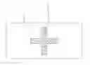
FIG. 1 is an isometric view of an insulating member according to the present invention;
FIG. 2 is an isometric view of the insulating member after coating as shown in FIG. 1; and
FIG. 3 is an isometric view of the semi-product of the chemical plating product according to the present invention.
DETAILED DESCRIPTION OF THE INVENTION
Reference will now be made to the drawings to describe the present invention in detail.
FIGS. 1 to 3 illustrate a method for forming a chemical plating product, includes: (a). provide an insulating member 1; (b). put the insulating member 1 into chemical solution to make it being chemical demoulded, and then make the surface of the insulating member 1 coarse; (c). plate the insulating member 1 to confirm the pre-plating scope 2 by coating catalyst, in this embodiment, the pre-plating scope 2 is configured with “+” shape; (d). chemical plating copper 3 on the pre-plating scope 2 to form semi-product. (e). form planar shaped organic nanopalladium metal conductive layer on the pre-plating scope 2 on the basis of step (c). (f). form stereo shaped nanopalladium metal conductive layer on the pre-plating scope 2 on the basis of step (c). (g). chemical plating copper, nickel and gold on the basis of step (d) to form product successively. (h). electro plating copper, nickel and gold on the basis of step of (d) to form product successively. (i). electro plating copper and nickel on the basis of step (d). (j). electro plating black nickel on the basis of step (i). (k). electro plating gold on the basis of step (i). Wherein make the surface of the insulating member 1 coarse to increase the bonding force between the coating metal layer and the insulating member 1. Wherein during the step of (g) to step of (k), due to the other scope of the insulating member 1 preclude the pre-plating scope 2 will not be plating with metal layer, thus can control the coating scope in the following steps. This method in this invention needs no laser carving machine to confirm the pre-plating scope 2, which reduce the cost.
Referring to FIGS. 1 to 3, the chemical plating product comprises an insulating member 1 and a metal coating covering the insulating member 1, the metal coating includes a pre-plating scope 2 formed by a coating catalyst and a chemical copper layer 3 covering the pre-plating scope 2. And make at least the pre-plating scope 2 of the insulating member 1 coarse.
The chemical plating product includes a planar shaped organic nanopalladium metal conductive layer on the pre-plating scope 2 or a stereo shaped nanopalladium metal conductive layer on the pre-plating scope 2.
In the first embodiment of the invention, chemical plating nickel and gold on the chemical copper layer. In the second embodiment of the invention, electro plating copper, nickel and gold on the chemical copper layer, due to electro plating nickel can prevent oxidation. In the third embodiment of the invention, electro plating copper, nickel and black nickel on the chemical copper layer, due to electro plating black nickel can add radio frequency of the product. In the fourth embodiment of the invention, electro plating copper, nickel and gold on the chemical copper layer to add the soldering feature.
While the preferred embodiments in accordance with the present invention has been shown and described, equivalent modifications and changes known to persons skilled in the art according to the spirit of the present invention are considered within the scope of the present invention as defined in the appended claims.
Claims
What is claimed is:1. A chemical plating product formed by chemical method, comprising:
an insulating member; and
a metal coating covering the insulative housing, the metal coating including a pre-plating scope formed by a coating catalyst and a chemical copper layer covering the pre-plating scope.
2. The chemical plating product as claimed in claim 1, wherein at least the pre-plating scope of the insulating member is chemical demoulded and is made coarse.
3. The chemical plating product as claimed in claim 2, wherein chemical plating nickel and gold on the chemical copper layer.
4. The chemical plating product as claimed in claim 2, wherein electro plating copper, nickel and gold on the chemical copper layer.
5. The chemical plating product as claimed in claim 2, wherein electro plating copper and nickel on the chemical copper layer.
6. The chemical plating product as claimed in claim 5, wherein electro plating black nickel on the electro plating nickel.
7. The chemical plating product as claimed in claim 1, wherein the coating catalyst is a planar shaped organic nanopalladium metal conductive layer.
8. The chemical plating product as claimed in claim 1, wherein the coating catalyst is a stereo shaped nanopalladium metal conductive layer.
9. A method for forming a chemical plating product, including:
(a). providing an insulating member;
(b). putting the insulating member into chemical solution to make it being chemical demoulded, and then make the surface of the insulating member coarse;
(c). plating the insulating member to confirm the pre-plating scope by coating catalyst;
(d). chemical-plating copper on the pre-plating scope.
10. The method for forming a chemical plating product as claimed in claim 9, wherein the coating catalyst in step (c) is a planar shaped organic nanopalladium metal conductive layer.
11. The method for forming a chemical plating product as claimed in claim 9, wherein the coating catalyst in step (c) is a stereo shaped nanopalladium metal conductive layer.
12. The method for forming a chemical plating product as claimed in claim 10, wherein chemical plating copper, nickel and gold on the basis of step (d).
13. The method for forming a chemical plating product as claimed in claim 10, wherein electro plating copper and nickel on the basis of step (d).
14. The method for forming a chemical plating product as claimed in claim 13, wherein electro plating black nickel on the electro plating nickel layer.
15. The method for forming a chemical plating product as claimed in claim 13, wherein electro plating gold the electro plating nickel layer.
16. A chemical plating product comprising:
an insulating member;
a coarse surface formed on the insulating member;
a catalyst layer coated upon a selected area of the coarse surface; and
a chemical copper layer covering the catalyst layer and no chemical copper layer is formed on other non-selected area of the coarse surface.
17. The chemical plating product as claimed in claim 16, further including a layers of gold, nickel and copper on the chemical copper layer.
Images & Drawings included:


Sources:
- United States Patent and Trademark Office - verify current appl. status at the USPTO↗
Recent applications in this class:
- » 20210381110 2021-12-09
Transient liquid phase bonding compositions and power electronics assemblies incorporating the same - » 20210140050 2021-05-13
Metallic coating and method - » 20200095684 2020-03-26
METHODS FOR INCREASING ADHESION BETWEEN METALLIC FILMS AND GLASS SURFACES AND ARTICLES MADE THEREFROM - » 20190249308 2019-08-15
Self-healing coatings for oil and gas applications - » 20190078212 2019-03-14
TRANSIENT LIQUID PHASE BONDING COMPOSITIONS AND POWER ELECTRONICS ASSEMBLIES INCORPORATING THE SAME - » 20180148844 2018-05-31
Deposition mask and method of manufacturing the same - » 20180051376 2018-02-22
Particulates and methods of making particulates - » 20170175271 2017-06-22
POLYMER COMPOSITION, INK COMPOSITION AND METHOD FOR SELECTIVELY METALLIZING INSULATING SUBSTRATE - » 20170081765 2017-03-23
Silver formation using stannous alkoxide complexes - » 20160177453 2016-06-23
METHOD OF PHOTOPOLYMERIZING OF ACRYLATES