Method of fabricating a uniformly aligned planar array of nanowires using atomic layer deposition
US20150132489A1
2015-05-14
14/479,760
2014-09-08
✅ Patent granted
US 9,702,059 B2
2017-07-11
-
-
Nina Bhat
2035-05-28
Abstract:
Invention for producing a relatively large uniformly aligned planar array of nanowires comprising:
-
- step 1) fabricating a template for producing nanowires in which the template comprises an alternating multilayer stack of thin film substrate layers and inert insulating thin film layers using atomic layer deposition; and
- step 2) fabricating a relatively large uniformly aligned planar array of nanowires by depositing atoms or molecules along the thin film substrate layers on at least one side of the template with the use of atomic layer deposition.
Applicant:
Interested in similar patents?
Get notified when new applications in this technology area are published.
Classification:
C23C16/45525 » CPC further
Chemical coating by decomposition of gaseous compounds, without leaving reaction products of surface material in the coating, i.e. chemical vapour deposition [CVD] processes characterised by the method of coating characterised by the method used for introducing gases into reaction chamber or for modifying gas flows in reaction chamber; Pulsed gas flow or change of composition over time Atomic layer deposition [ALD]
C23C16/04 » CPC main
Chemical coating by decomposition of gaseous compounds, without leaving reaction products of surface material in the coating, i.e. chemical vapour deposition [CVD] processes Coating on selected surface areas, e.g. using masks
C23C16/455 IPC
Chemical coating by decomposition of gaseous compounds, without leaving reaction products of surface material in the coating, i.e. chemical vapour deposition [CVD] processes characterised by the method of coating characterised by the method used for introducing gases into reaction chamber or for modifying gas flows in reaction chamber
C30B25/18 IPC
Single-crystal growth by chemical reaction of reactive gases, e.g. chemical vapour-deposition growth; Epitaxial-layer growth characterised by the substrate
C30B25/186 » CPC further
Single-crystal growth by chemical reaction of reactive gases, e.g. chemical vapour-deposition growth; Epitaxial-layer growth characterised by the substrate being specially pre-treated by, e.g. chemical or physical means
C23C16/00 IPC
Chemical deposition or plating by decomposition; Contact plating
C23C16/00 IPC
Chemical coating by decomposition of gaseous compounds, without leaving reaction products of surface material in the coating, i.e. chemical vapour deposition [CVD] processes
C30B25/04 » CPC main
Single-crystal growth by chemical reaction of reactive gases, e.g. chemical vapour-deposition growth; Epitaxial-layer growth Pattern deposit, e.g. by using masks
C30B29/60 » CPC further
Single crystals or homogeneous polycrystalline material with defined structure characterised by the material or by their shape characterised by shape
Description
BACKGROUND OF THE INVENTION
1. Field of the Invention
In general, the field of the present invention pertains to methods of fabricating nanowires. More specifically, the field of the present invention pertains to scalable methods of fabricating uniformly aligned planar arrays of nanowires.
2. Prior Art
Prior art pertinent to the present invention includes bottom-up and top-down methods of fabricating nanowires. Wherein, such prior art methods have their respective disadvantages with respect to the structure, function, and/or scalability of the nanowires which are fabricated. The method of fabricating nanowires in the present invention proposes to have advantages over pertinent prior art with respect to the structure, function, and/or scalability of the nanowires fabricated by applying a scalable method of fabricating a uniformly aligned planar array of functional nanowires.
SUMMARY OF THE INVENTION
In the preferred embodiment of the present invention, a relatively large uniformly aligned planar array of nanowires is fabricated by steps which include:
Step 1) Fabricating a template for producing nanowires in which the template comprises a multilayer stack of thin films which include thin film substrate layers which alternate with inert insulating thin film layers using atomic layer deposition; and
Step 2) Fabricating a relatively large uniformly aligned planar array of nanowires by depositing atoms or molecules along the thin film substrate layers on one side of the template with the use of atomic layer deposition.
In other preferred embodiments of the present invention, the configuration of the nanowires can be shaped by fabricating the template on a mold which has the desired shape. Wherein, the nanowires (and their respective template) would consequentially have their desired shape upon fabricating the nanowires on the shaped template.
BRIEF DESCRIPTION OF THE DRAWINGS
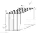
FIG. (1a) illustrates a nanowire template comprising an alternating multilayer stack of thin film substrate layers and inert insulating thin film layers produced from atomic layer deposition.
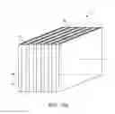
FIG. (1b) illustrates the nanowires formed on the nanowire template (illustrated in FIG. 1a) as produced by atomic layer deposition upon the substrate layers along one side of the template after the nanowire template, which is illustrated in FIG. (1a), is rotated 90 degrees.
DETAILED DESCRIPTION OF THE INVENTION
Invention for producing a relatively large uniformly aligned planar array of nanowires comprising steps which include:
Step 1) Fabricating the nanowire template (2) illustrated in FIG. (1a) using atomic layer deposition. In which case, the template comprises an alternating multilayer stack of thin film layers comprising: a) thin film substrate layers comprising, for example, a silicon-based substrate material, as illustrated, for example, by layers (4a) and (4b) in FIG. 1a); and b) inert insulating thin film layers comprising, for example, a silicon-based insulating material (which will not chemisorb the precursor applied in step 2 during the formation of the nanowires), as illustrated, for example, by layers (6a) and (6b) in FIG. (1a).
Wherein, the thin film substrate layers produced in the atomic layer deposition process in step (1) will become growth substrate layers for producing nanowires in step (2). (Note that the thick dashed line illustrated in FIG. 1a) is intended to indicate that the stack of thin film layers can include more thin film layers than the amount illustrated.); and
Step 2) Fabricating a relatively large uniformly aligned planar array of nanowires as illustrated, for example, by nanowires (8a and 8b) in FIG. (1b), by depositing atoms or molecules, by way of atomic layer deposition, along the thin film growth substrates on side (2′) of the template after rotating template (2) illustrated in FIG. 1a) 90 degrees to its position as illustrated in FIG. 1b). Note that the width of a nanowire, or a portion of a nanowire, and the width of an inert insulating layer, or a portion of an inert insulating layer, can be controlled in step (1) by the number of cycles of atomic layer deposition which is applied to form any respective layer, or portion of a layer, e.g., with the use of a masking technique for controlling the width of a portion of a nanowire or an inert insulating layer. Also, note that the thick dashed line illustrated in FIG. (1b) is intended to indicate that the composite of thin film layers and respective nanowires can include more thin film layers and respective nanowires than the amount illustrated. Furthermore, note that only the hidden outer edges of the template in FIGS. (1a) and (1b) are illustrated with dashed lines.
In other preferred embodiments of the present invention, the configuration of the nanowires can be shaped by fabricating the template on a mold which has the desired shape. Wherein, the nanowires (and their respective template) would consequentially have their desired shape upon fabricating the nanowires on the shaped template.
To broaden, the detailed description of the present invention herein describes a limited number of the embodiments of the present invention. Yet, various other embodiments of the present invention can be included in the scope of the present invention. Thus, the present invention should be interpreted in as broad a scope as possible so as to include all the equivalent embodiments of the present invention.
Claims
I claim:1. Method of fabricating a uniformly aligned planar array of nanowires comprising the steps of:
1) fabricating a template for producing nanowires using a first atomic layer deposition process, wherein the template comprises an alternating multilayer stack of thin film substrate layers and inert insulating thin film layers; and
2) fabricating the uniformly aligned planar array of nanowires by depositing particles selected from the group of atoms and molecules along the thin film substrate layers on at least one side of the template using a second atomic layer deposition process, such that the inert thin film layers resist chemisorption of the precursor particles applied to produce the nanowires in the second atomic layer deposition process.
Images & Drawings included:
Sources:
- United States Patent and Trademark Office - verify current appl. status at the USPTO↗
Recent applications in this class:
- » 20250283212 2025-09-11
INHERENTLY SELECTIVE THERMAL ATOMIC LAYER DEPOSITION OF COPPER METAL FILMS - » 20250277305 2025-09-04
Selective Thin Film Deposition Method Using Area-Selective Atomic Layer Deposition Method, and Substrates Having Thin Films Selectively Formed Thereon - » 20250263831 2025-08-21
FILM FORMING METHOD AND FILM FORMING APPARATUS - » 20250263830 2025-08-21
METHOD OF FORMING CARBON-BASED FILM AND FILM FORMING APPARATUS - » 20250257446 2025-08-14
FILM-FORMING METHOD AND SUBSTRATE-PROCESSING DEVICE - » 20250230539 2025-07-17
METHOD FOR MANUFACTURING MODIFIED SUBSTRATE AND METHOD FOR MANUFACTURING SEMICONDUCTOR DEVICE - » 20250223688 2025-07-10
METHOD AND APPARATUS FOR AREA-SELECTIVE DEPOSITION - » 20250215555 2025-07-03
METHODS AND ASSEMBLIES FOR SELECTIVE DEPOSITION OF METAL-CONTAINING MATERIAL - » 20250215554 2025-07-03
UNIFORM COATING OF A SURFACE - » 20250188599 2025-06-12
SHIELDING COMPOUND, METHOD OF FORMING THIN FILM USING SHIELDING COMPOUND, SEMICONDUCTOR SUBSTRATE FABRICATED USING METHOD, AND SEMICONDUCTOR DEVICE INCLUDING SEMICONDUCTOR SUBSTRATE