Structure and method for 3D IC package
US20150194361A1
2015-07-09
14/664,057
2015-03-20
✅ Patent granted
US 9,412,678 B2
2016-08-09
-
-
Yasser A Abdelaziez
Slater Matsil, LLP
2035-03-20
Abstract:
A chip package may include: a first die; a second die; an underfill disposed between and in physical contact with the first die and the second die; and one or more conductive elements encapsulated in the underfill and coupling the first die and the second die to each other.
Inventors:
- Chen-Hua Yu 635 🇹🇼 Hsin-Chu, Taiwan
- Shin-Puu Jeng 176 🇹🇼 Hsin-Chu, Taiwan
- Shang-Yun HOU 180 🇹🇼 Jubei City, Taiwan
- Der-Chyang Yeh 135 🇹🇼 Hsin-Chu, Taiwan
- Shang-Yun Hou 194 🇹🇼 Jubei, Taiwan
Assignee:
- TAIWAN SEMICONDUCTOR MANUFACTURING COMPANY, LTD. 8,890 🇹🇼 Hsin-Chu, Taiwan
Applicant:
Interested in similar patents?
Get notified when new applications in this technology area are published.
Classification:
H01L23/3157 » CPC main
Details of semiconductor or other solid state devices; Encapsulations, e.g. encapsulating layers, coatings, e.g. for protection characterised by the arrangement or shape Partial encapsulation or coating
H01L21/561 » CPC further
Processes or apparatus adapted for the manufacture or treatment of semiconductor or solid state devices or of parts thereof; Manufacture or treatment of semiconductor devices or of parts thereof the devices having at least one potential-jump barrier or surface barrier, e.g. PN junction, depletion layer or carrier concentration layer; Assembly of semiconductor devices using processes or apparatus not provided for in a single one of the subgroups - , e.g. sealing of a cap to a base of a container; Encapsulations, e.g. encapsulation layers, coatings Batch processing
H01L21/563 » CPC further
Processes or apparatus adapted for the manufacture or treatment of semiconductor or solid state devices or of parts thereof; Manufacture or treatment of semiconductor devices or of parts thereof the devices having at least one potential-jump barrier or surface barrier, e.g. PN junction, depletion layer or carrier concentration layer; Assembly of semiconductor devices using processes or apparatus not provided for in a single one of the subgroups - , e.g. sealing of a cap to a base of a container; Encapsulations, e.g. encapsulation layers, coatings Encapsulation of active face of flip-chip device, e.g. underfilling or underencapsulation of flip-chip, encapsulation preform on chip or mounting substrate
H01L21/565 » CPC further
Processes or apparatus adapted for the manufacture or treatment of semiconductor or solid state devices or of parts thereof; Manufacture or treatment of semiconductor devices or of parts thereof the devices having at least one potential-jump barrier or surface barrier, e.g. PN junction, depletion layer or carrier concentration layer; Assembly of semiconductor devices using processes or apparatus not provided for in a single one of the subgroups - , e.g. sealing of a cap to a base of a container; Encapsulations, e.g. encapsulation layers, coatings Moulds
H01L21/568 » CPC further
Processes or apparatus adapted for the manufacture or treatment of semiconductor or solid state devices or of parts thereof; Manufacture or treatment of semiconductor devices or of parts thereof the devices having at least one potential-jump barrier or surface barrier, e.g. PN junction, depletion layer or carrier concentration layer; Assembly of semiconductor devices using processes or apparatus not provided for in a single one of the subgroups - , e.g. sealing of a cap to a base of a container; Encapsulations, e.g. encapsulation layers, coatings Temporary substrate used as encapsulation process aid
H01L21/6835 » CPC further
Processes or apparatus adapted for the manufacture or treatment of semiconductor or solid state devices or of parts thereof; Apparatus specially adapted for handling semiconductor or electric solid state devices during manufacture or treatment thereof; Apparatus specially adapted for handling wafers during manufacture or treatment of semiconductor or electric solid state devices or components ; Apparatus not specifically provided for elsewhere for supporting or gripping using temporarily an auxiliary support
H01L21/76898 » CPC further
Processes or apparatus adapted for the manufacture or treatment of semiconductor or solid state devices or of parts thereof; Manufacture or treatment of devices consisting of a plurality of solid state components formed in or on a common substrate or of parts thereof; Manufacture of integrated circuit devices or of parts thereof; Manufacture of specific parts of devices defined in group; Applying interconnections to be used for carrying current between separate components within a device comprising conductors and dielectrics formed through a semiconductor substrate
H01L23/3114 » CPC further
Details of semiconductor or other solid state devices; Encapsulations, e.g. encapsulating layers, coatings, e.g. for protection characterised by the arrangement or shape the device being completely enclosed the device being a chip scale package, e.g. CSP
H01L23/3135 » CPC further
Details of semiconductor or other solid state devices; Encapsulations, e.g. encapsulating layers, coatings, e.g. for protection characterised by the arrangement or shape the device being completely enclosed Double encapsulation or coating and encapsulation
H01L23/3142 » CPC further
Details of semiconductor or other solid state devices; Encapsulations, e.g. encapsulating layers, coatings, e.g. for protection characterised by the arrangement or shape the device being completely enclosed Sealing arrangements between parts, e.g. adhesion promotors
H01L23/49816 » CPC further
Details of semiconductor or other solid state devices; Arrangements for conducting electric current to or from the solid state body in operation, e.g. leads, terminal arrangements ; Selection of materials therefor consisting of soldered constructions; Leads, on insulating substrates,; Additional leads joined to the metallisation on the insulating substrate, e.g. pins, bumps, wires, flat leads Spherical bumps on the substrate for external connection, e.g. ball grid arrays [BGA]
H01L23/49827 » CPC further
Details of semiconductor or other solid state devices; Arrangements for conducting electric current to or from the solid state body in operation, e.g. leads, terminal arrangements ; Selection of materials therefor consisting of soldered constructions; Leads, on insulating substrates, Via connections through the substrates, e.g. pins going through the substrate, coaxial cables
H01L23/49838 » CPC further
Details of semiconductor or other solid state devices; Arrangements for conducting electric current to or from the solid state body in operation, e.g. leads, terminal arrangements ; Selection of materials therefor consisting of soldered constructions; Leads, on insulating substrates, Geometry or layout
H01L23/5389 » CPC further
Details of semiconductor or other solid state devices; Arrangements for conducting electric current within the device in operation from one component to another, i.e. interconnections, e.g. wires, lead frames the interconnection structure between a plurality of semiconductor chips being formed on, or in, insulating substrates the chips being integrally enclosed by the interconnect and support structures
H01L24/11 » CPC further
Arrangements for connecting or disconnecting semiconductor or solid-state bodies; Methods or apparatus related thereto; Means for bonding being attached to, or being formed on, the surface to be connected, e.g. chip-to-package, die-attach, "first-level" interconnects; Manufacturing methods related thereto; Bump connectors ; Manufacturing methods related thereto Manufacturing methods
H01L24/81 » CPC further
Arrangements for connecting or disconnecting semiconductor or solid-state bodies; Methods or apparatus related thereto; Methods for connecting semiconductor or other solid state bodies using means for bonding being attached to, or being formed on, the surface to be connected using a bump connector
H01L24/96 » CPC further
Arrangements for connecting or disconnecting semiconductor or solid-state bodies; Methods or apparatus related thereto; Batch processes at chip-level, i.e. with connecting carried out on a plurality of singulated devices, i.e. on diced chips the devices being encapsulated in a common layer, e.g. neo-wafer or pseudo-wafer, said common layer being separable into individual assemblies after connecting
H01L24/97 » CPC further
Arrangements for connecting or disconnecting semiconductor or solid-state bodies; Methods or apparatus related thereto; Batch processes at chip-level, i.e. with connecting carried out on a plurality of singulated devices, i.e. on diced chips the devices being connected to a common substrate, e.g. interposer, said common substrate being separable into individual assemblies after connecting
H01L25/0655 » CPC further
Assemblies consisting of a plurality of individual semiconductor or other solid state devices ; Multistep manufacturing processes thereof all the devices being of a type provided for in the same subgroup of groups - , e.g. assemblies of rectifier diodes the devices not having separate containers the devices being of a type provided for in group the devices being arranged next to each other
H01L25/0657 » CPC further
Assemblies consisting of a plurality of individual semiconductor or other solid state devices ; Multistep manufacturing processes thereof all the devices being of a type provided for in the same subgroup of groups - , e.g. assemblies of rectifier diodes the devices not having separate containers the devices being of a type provided for in group Stacked arrangements of devices
H01L25/50 » CPC further
Assemblies consisting of a plurality of individual semiconductor or other solid state devices ; Multistep manufacturing processes thereof Multistep manufacturing processes of assemblies consisting of devices, each device being of a type provided for in group or
H01L24/13 » CPC further
Arrangements for connecting or disconnecting semiconductor or solid-state bodies; Methods or apparatus related thereto; Means for bonding being attached to, or being formed on, the surface to be connected, e.g. chip-to-package, die-attach, "first-level" interconnects; Manufacturing methods related thereto; Bump connectors ; Manufacturing methods related thereto; Structure, shape, material or disposition of the bump connectors prior to the connecting process of an individual bump connector
H01L25/03 » CPC further
Assemblies consisting of a plurality of individual semiconductor or other solid state devices ; Multistep manufacturing processes thereof all the devices being of a type provided for in the same subgroup of groups - , e.g. assemblies of rectifier diodes
H01L2224/0401 » CPC further
Indexing scheme for arrangements for connecting or disconnecting semiconductor or solid-state bodies and methods related thereto as covered by; Means for bonding being attached to, or being formed on, the surface to be connected, e.g. chip-to-package, die-attach, "first-level" interconnects; Manufacturing methods related thereto; Bonding areas; Manufacturing methods related thereto; Structure, shape, material or disposition of the bonding areas prior to the connecting process Bonding areas specifically adapted for bump connectors, e.g. under bump metallisation [UBM]
H01L2224/04105 » CPC further
Indexing scheme for arrangements for connecting or disconnecting semiconductor or solid-state bodies and methods related thereto as covered by; Means for bonding being attached to, or being formed on, the surface to be connected, e.g. chip-to-package, die-attach, "first-level" interconnects; Manufacturing methods related thereto; Bonding areas; Manufacturing methods related thereto; Structure, shape, material or disposition of the bonding areas prior to the connecting process Bonding areas formed on an encapsulation of the semiconductor or solid-state body, e.g. bonding areas on chip-scale packages
H01L2224/12105 » CPC further
Indexing scheme for arrangements for connecting or disconnecting semiconductor or solid-state bodies and methods related thereto as covered by; Means for bonding being attached to, or being formed on, the surface to be connected, e.g. chip-to-package, die-attach, "first-level" interconnects; Manufacturing methods related thereto; Bump connectors; Manufacturing methods related thereto; Structure, shape, material or disposition of the bump connectors prior to the connecting process Bump connectors formed on an encapsulation of the semiconductor or solid-state body, e.g. bumps on chip-scale packages
H01L2224/1703 » CPC further
Indexing scheme for arrangements for connecting or disconnecting semiconductor or solid-state bodies and methods related thereto as covered by; Means for bonding being attached to, or being formed on, the surface to be connected, e.g. chip-to-package, die-attach, "first-level" interconnects; Manufacturing methods related thereto; Bump connectors; Manufacturing methods related thereto; Structure, shape, material or disposition of the bump connectors after the connecting process of a plurality of bump connectors; Structure Bump connectors having different sizes, e.g. different diameters, heights or widths
H01L2224/73204 » CPC further
Indexing scheme for arrangements for connecting or disconnecting semiconductor or solid-state bodies and methods related thereto as covered by; Means for bonding being of different types provided for in two or more of groups; Location after the connecting process on the same surface; Bump and layer connectors the bump connector being embedded into the layer connector
H01L2224/73259 » CPC further
Indexing scheme for arrangements for connecting or disconnecting semiconductor or solid-state bodies and methods related thereto as covered by; Means for bonding being of different types provided for in two or more of groups; Location after the connecting process on different surfaces Bump and HDI connectors
H01L2224/81005 » CPC further
Indexing scheme for arrangements for connecting or disconnecting semiconductor or solid-state bodies and methods related thereto as covered by; Methods for connecting semiconductor or other solid state bodies using means for bonding being attached to, or being formed on, the surface to be connected using a bump connector involving a temporary auxiliary member not forming part of the bonding apparatus being a temporary or sacrificial substrate
H01L2224/81193 » CPC further
Indexing scheme for arrangements for connecting or disconnecting semiconductor or solid-state bodies and methods related thereto as covered by; Methods for connecting semiconductor or other solid state bodies using means for bonding being attached to, or being formed on, the surface to be connected using a bump connector; Arrangement of the bump connectors prior to mounting wherein the bump connectors are disposed on both the semiconductor or solid-state body and another item or body to be connected to the semiconductor or solid-state body
H01L2224/81986 » CPC further
Indexing scheme for arrangements for connecting or disconnecting semiconductor or solid-state bodies and methods related thereto as covered by; Methods for connecting semiconductor or other solid state bodies using means for bonding being attached to, or being formed on, the surface to be connected using a bump connector Specific sequence of steps, e.g. repetition of manufacturing steps, time sequence
H01L2224/83104 » CPC further
Indexing scheme for arrangements for connecting or disconnecting semiconductor or solid-state bodies and methods related thereto as covered by; Methods for connecting semiconductor or other solid state bodies using means for bonding being attached to, or being formed on, the surface to be connected using a layer connector the layer connector being supplied to the parts to be connected in the bonding apparatus by applying pressure, e.g. by injection
H01L2224/9202 » CPC further
Indexing scheme for arrangements for connecting or disconnecting semiconductor or solid-state bodies and methods related thereto as covered by; Methods for connecting semiconductor or solid state bodies including different methods provided for in two or more of groups - ; Specific sequence of method steps Forming additional connectors after the connecting process
H01L2224/96 » CPC further
Indexing scheme for arrangements for connecting or disconnecting semiconductor or solid-state bodies and methods related thereto as covered by; Batch processes at chip-level, i.e. with connecting carried out on a plurality of singulated devices, i.e. on diced chips the devices being encapsulated in a common layer, e.g. neo-wafer or pseudo-wafer, said common layer being separable into individual assemblies after connecting
H01L2224/97 » CPC further
Indexing scheme for arrangements for connecting or disconnecting semiconductor or solid-state bodies and methods related thereto as covered by; Batch processes at chip-level, i.e. with connecting carried out on a plurality of singulated devices, i.e. on diced chips the devices being connected to a common substrate, e.g. interposer, said common substrate being separable into individual assemblies after connecting
H01L2225/06513 » CPC further
Details relating to assemblies covered by the group but not provided for in its subgroups; All the devices being of a type provided for in the same subgroup of groups - the devices not having separate containers the devices being of a type provided for in group; Stacked arrangements of devices Bump or bump-like direct electrical connections between devices, e.g. flip-chip connection, solder bumps
H01L2225/06541 » CPC further
Details relating to assemblies covered by the group but not provided for in its subgroups; All the devices being of a type provided for in the same subgroup of groups - the devices not having separate containers the devices being of a type provided for in group; Stacked arrangements of devices Conductive via connections through the device, e.g. vertical interconnects, through silicon via [TSV]
H01L2924/12042 » CPC further
Indexing scheme for arrangements or methods for connecting or disconnecting semiconductor or solid-state bodies as covered by; Details of semiconductor or other solid state devices to be connected; Device type; Passive devices, e.g. 2 terminal devices; Optical Diode LASER
H01L2924/181 » CPC further
Indexing scheme for arrangements or methods for connecting or disconnecting semiconductor or solid-state bodies as covered by; Details of package parts other than the semiconductor or other solid state devices to be connected Encapsulation
H01L23/31 IPC
Details of semiconductor or other solid state devices; Encapsulations, e.g. encapsulating layers, coatings, e.g. for protection characterised by the arrangement or shape
H01L21/56 IPC
Processes or apparatus adapted for the manufacture or treatment of semiconductor or solid state devices or of parts thereof; Manufacture or treatment of semiconductor devices or of parts thereof the devices having at least one potential-jump barrier or surface barrier, e.g. PN junction, depletion layer or carrier concentration layer; Assembly of semiconductor devices using processes or apparatus not provided for in a single one of the subgroups - , e.g. sealing of a cap to a base of a container Encapsulations, e.g. encapsulation layers, coatings
H01L23/538 IPC
Details of semiconductor or other solid state devices; Arrangements for conducting electric current within the device in operation from one component to another, i.e. interconnections, e.g. wires, lead frames the interconnection structure between a plurality of semiconductor chips being formed on, or in, insulating substrates
H01L21/683 IPC
Processes or apparatus adapted for the manufacture or treatment of semiconductor or solid state devices or of parts thereof; Apparatus specially adapted for handling semiconductor or electric solid state devices during manufacture or treatment thereof; Apparatus specially adapted for handling wafers during manufacture or treatment of semiconductor or electric solid state devices or components ; Apparatus not specifically provided for elsewhere for supporting or gripping
H01L23/00 IPC
Details of semiconductor or other solid state devices
H01L25/065 IPC
Assemblies consisting of a plurality of individual semiconductor or other solid state devices ; Multistep manufacturing processes thereof all the devices being of a type provided for in the same subgroup of groups - , e.g. assemblies of rectifier diodes the devices not having separate containers the devices being of a type provided for in group
H01L21/768 IPC
Processes or apparatus adapted for the manufacture or treatment of semiconductor or solid state devices or of parts thereof; Manufacture or treatment of devices consisting of a plurality of solid state components formed in or on a common substrate or of parts thereof; Manufacture of integrated circuit devices or of parts thereof; Manufacture of specific parts of devices defined in group Applying interconnections to be used for carrying current between separate components within a device comprising conductors and dielectrics
H01L25/00 IPC
Assemblies consisting of a plurality of individual semiconductor or other solid state devices ; Multistep manufacturing processes thereof
H01L23/498 IPC
Details of semiconductor or other solid state devices; Arrangements for conducting electric current to or from the solid state body in operation, e.g. leads, terminal arrangements ; Selection of materials therefor consisting of soldered constructions Leads, on insulating substrates,
Description
PRIORITY CLAIM AND CROSS-REFERENCE
This application is a divisional of U.S. patent application Ser. No. 13/791,305, entitled “Structure and Method for 3D IC Package,” filed on Mar. 8, 2013, which application is hereby incorporated herein by reference.
BACKGROUND
Since the invention of the integrated circuit (IC), the semiconductor industry has experienced rapid growth due to continuous improvements in the integration density of various electronic components (i.e., transistors, diodes, resistors, capacitors, etc.). For the most part, this improvement in integration density has come from repeated reductions in minimum feature size, which allows more components to be integrated into a given area.
These integration improvements are essentially two-dimensional (2D) in nature, in that the volume occupied by the integrated components is essentially on the surface of the semiconductor wafer. Although dramatic improvement in lithography has resulted in considerable improvement in 2D IC formation, there are physical limits to the density that can be achieved in two dimensions. One of these limits is the minimum size needed to make these components. Also, when more devices are put into one chip, more complex designs are required.
In an attempt to further increase circuit density, three-dimensional (3D) ICs have been investigated. In a typical formation process of a 3D IC, two dies are bonded together and electrical connections are formed between each die and contact pads on a substrate. Interposer stacking is part of 3D IC technology, where a Through-Silicon-Via (TSV) embedded interposer is connected to a device silicon with a micro bump. 3D IC manufacturing process flows can be separated into two types. In a chip-on-chip-on-substrate (CoCoS) process flow, a silicon interposer chip is first attached onto a packaging substrate, and then a different device silicon chips is attached onto the interposer. In a chip-on-wafer-on-substrate (CoWoS) process flow, a device silicon chip is first attached onto a silicon interposer wafer, which is then diced. The resulting stacked silicon is then attached onto a substrate.
BRIEF DESCRIPTION OF THE DRAWINGS
For a more complete understanding of the present embodiments, and the advantages thereof, reference is now made to the following descriptions taken in conjunction with the accompanying drawings, in which:
FIG. 1 illustrates a cross section of a chip package according to an embodiment; and
FIGS. 2a through 2h illustrate a process of forming the chip package of FIG. 1 according to an embodiment.
DETAILED DESCRIPTION OF ILLUSTRATIVE EMBODIMENTS
The making and using of the present embodiments are discussed in detail below. It should be appreciated, however, that the present disclosure provides many applicable inventive concepts that can be embodied in a wide variety of specific contexts. The specific embodiments discussed are merely illustrative of specific ways to make and use the disclosed subject matter, and do not limit the scope of the different embodiments.
Described herein are embodiments of a chip package structure and a method for forming the chip package. The chip package can be used as a component in 3D IC manufacturing and may be overlaid on a substrate, a board, a wafer, or other chips or chip packages. For example, the chip package may comprise a memory device or component, a processor, other chip logic, or a combination thereof. The chip package may comprise a second chip or die positioned on a first chip or die using a CoWoS like process flow. The process flow provides wafer level packaging that skips using a substrate bonding step as in a typical CoWoS process flow.
The second die may be larger than the first die, and thus may form an overhang structure when placed on the first die during the manufacturing process. To support this overhang structure, the first die may be encapsulated in a first molding compound. After the larger second die is positioned on and electrically coupled to the first die (encapsulated in the first molding compound), an underfill may be injected between the two stacked dies. The second die and the underfill may then be encapsulated in a second molding compound over the first molding compound encapsulating the first die. The second molding compound on the first molding compound and the underfill injected between the second and first dies may provide reliable mechanical support to the overhang structure, which avoids package handling issues during the manufacturing process, such as warping. A interconnect layer or structure comprising a plurality of connectors, such as a ball grid array (BGA), may then be coupled to the first die using a redistribution layer (RDL) or the like, which is placed between the first die and the interconnect layer or structure. The resulting package provides a 3D fan-out structure.
Embodiments are described herein with respect to a specific context, namely a chip package built using a CoWoS like process flow that provides packaging level that skips a substrate bonding step typical of CoWoS process flows. The chip package comprises a system-on-chip (SoC) encapsulated in a first molding compound, and a larger chip placed on an underfill on the SoC die and encapsulated in a second molding compound on the first molding compound. The chip package also includes an interconnect structure with connectors, such as a BGA, coupled to the chip through a RDL. Other embodiments may also be applied, such as for other stacked chips/dies with an overhang structure that is supported using molding compound and underfill layers and fabricated using a similar process flow with packaging level that skips substrate bonding.
Throughout the various figures and discussion, like reference numbers refer to like components. Also, although singular components may be depicted throughout some of the figures, this is for simplicity of illustration and ease of discussion. A person having ordinary skill in the art will readily appreciate that such discussion and depiction can be and usually is applicable for many components within a structure.
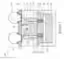
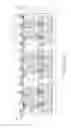
FIG. 1 illustrates a cross section of a chip package 100, according to an embodiment. The chip package 100 may include stacked chips or dies and other interconnect components. The chip package 100 may comprise a die or chip 120 coupled to a second die or chip 110, e.g., a system on chip (SoC), through an underfill 70. The second chip 110 may be encapsulated in a first molding compound 30. The chip 120 may be encapsulated with the underfill 70 in a second molding compound 94 in contact with the first molding compound 30. The second chip 110 (encapsulated in the first molding compound 30) may be coupled on the side opposite to the underfill 70 to a BGA 46 through a RDL 29. In other embodiments, other dies, chips, or chip packages may be included. Other connectors, interconnect structure, or interconnect layer may also be used instead of the BGA 46.
The second chip 110 may comprise a chip system 20 attached to a semiconductor substrate 10. The chip system 20 may comprise one or more stacked chips or chip logic, which may comprise one or more stacked dielectric, conductive, and/or semiconductor layers. For example, the stacked chips or chip logic may correspond to one or more overlaid memory devices (e.g., flash memory and DRAM memory), one or more processors or processor cores (e.g., CPU cores), other digital logic, or combinations thereof. The semiconductor substrate 10 may be a silicon substrate. The chip system 20 may also comprise any number of through vias and pads 22 that extend laterally and vertically in the stacked layers or chips of the chip system 20. The semiconductor substrate 10 may comprise second through vias 12 that are coupled to the through vias and pads 22 in the chip system 20.
The chip 120 may comprise one or more layers 90 (e.g., semiconductor, dielectric, and/or conductive layers) attached to a second semiconductor substrate 92. The one or more layers 90 may comprise a simpler logic than the chip system 20. The first molding compound 30 that encapsulates the second chip 110 and the second molding compound 94 that encapsulates the chip 120 may be similar or different polymers, molding underfill, or the like. In other embodiments, any two dies may be coupled to each other through the underfill 70. For example, a second SoC die may be coupled to the second chip 110 instead of the chip 120. A simple logic chip (e.g., a single layer on substrate) may also be coupled to the chip 120 instead of the second chip 110.
The underfill 70 may be a polymer, such as commercially available epoxy, placed (e.g., injected) between the second chip 110 and the chip 120. The underfill 70 may encapsulate conductive elements 60 (made of metal or any conductor) coupled to the second through vias 12 of the second chip 110, for example through Under-Bump Metallization (UBM) elements 62. The underfill 70 may also encapsulate second conductive elements 80 coupled to the one or more layers 90 of the chip 120, for example through second UBM elements 82. The conductive elements 60 may be aligned and coupled to the second conductive elements 80 through solder balls or bumps 72 or the like, without using an interposer between the chip 120 and the second chip 110. Thus, the conductive elements 60 and the second conductive elements 80 provide electrical coupling between the second chip 110 and the chip 120.
The RDL 29 may comprise a patterned conductive layer 26 coupled to the through vias and pads 22 of the chip system 20, and a polymer layer 27 on the patterned conductive layer 26, the second chip 110, and the first molding compound 30. The BGA 46 may include a plurality of conductive structures 44, such as conductive spheres or microbumps, which may be arranged in an array (or other orderly pattern) and attached to the patterned conductive layer 26 of the RDL 29, e.g., through third UBM elements 28. As such, the patterned conductive layer 26 provide electrical coupling between the BGA 46 and the second chip 110.
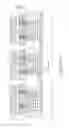
FIGS. 2a through 2h illustrate a process flow to form the chip package 100 according to an embodiment. Although this embodiment is discussed with steps performed in a particular order, steps may be performed in any logical order. FIG. 2a illustrates a step of obtaining of a SoC wafer with through vias comprising an array or series of adjacent and repeated patterns (each corresponding to a second chip 110). The SoC wafer with through vias may be made using any suitable fabrication process, where the second through vias 12 in the semiconductor substrate 10 and the through vias and pads 22 of the chip system 20 may be filled with metal or conductive material. The top surface of the chip system 20 may also include openings 23 that expose the through vias and pads 22.
FIG. 2b illustrates reconfiguration and molding steps. The steps include separating the SoC wafer into separate individual dies or second chips 110, e.g., using a chip saw, patterned etch, laser, or the like step. The individual second chips 110 may then be bonded to a carrier 50 through an adhesive layer 40. The adhesive layer 40 may be disposed, for example laminated, on the carriers 50. The second chips 110 may be placed with a spacing between the individual second chips 110 on the carrier 50. The adhesive layer 40 may be formed of a glue or may be a lamination layer formed of a foil. The carrier 50 may be any suitable substrate that provides (during intermediary steps of the fabrication process) mechanical support for the layers on top. The carrier 50 may be, for example, a silicon substrate, a silicon or glass interposer, a printed circuit board (PCB), an organic laminate substrate, or the like. In other embodiments, other types of chip packages or dies may be placed on the adhesive layer 40. The second chips 110 may be formed on the adhesive layer 40 or placed using any suitable method of placing the second chips 110 onto the adhesive layer 40 and integrating the second chips 110 into a manufacturing process flow. The first molding compound 30 may be formed to encapsulate the second chips 110 on the adhesive layer 40. The first molding compound 30 may be a polymer, a molding underfill, the like, or a combination thereof. The first molding compound 30 may be formed by injecting the first molding compound 30 to envelope the second chips 110 on the adhesive layer 40.
FIG. 2c illustrates steps for adding through vias protrusion and uBumps to the second chips 110. The steps includes grinding the first molding compound 30 to expose the top surface of the second chips 110, and extending the second through vias 12 to the exposed surface of the semiconductor substrate 10, e.g., using etching, patterning processes, laser, or other processes for making through vias. The conductive elements 60 may be placed (e.g., deposited) on the extended second through vias 12 at the surface level of the semiconductor substrates 10 of the second chips 110. The solder balls or bumps 72 or the like may then be placed (e.g., deposited) on the conductive elements 60.
FIG. 2d illustrates chip joint and underfill injection steps. The second conductive elements 80 may be placed on the chips 120 before placing the chips 120 on the second chips 110. The chips 120 may be placed using any suitable method of placing the chips 120 on the second chips 110. The chips 120 may be aligned on the respective second chips 110 to allow coupling between the second conductive elements 80 and the conductive elements 60 (through the bumps 72). Thus, the chips 120 and the second chips 110 are coupled to each other without using an interposer (e.g., a wafer). The chips 120 may be larger than the second chips 110, resulting in an overhang structure when placed on the second chips 110. The underfill 70 may then be injected between each connected pair of chips 120 and second chips 110, which provides better support to the chips 120 overhang over the second chips 110.
FIG. 2e illustrates a molding step, where the second molding compound 94 may be formed to encapsulate the chips 120 on the first molding compound 30. The second molding compound 94 may be a polymer, a molding underfill, the like, or a combination thereof. The second molding compound 94 may be formed by injecting the second molding compound 94 to envelope the chips 120 and the underfill 70 on the second chips 110 and the first molding compound 30.
FIG. 2f illustrates a carrier de-bond step, where the carrier 50 and the adhesive layer 40 are removed. The carrier 50 may be removed by dissolving or etching the adhesive layer 40 that bonds the carrier 50 to the other components/layers. Further, the chip package may be flipped. The remaining bonded layers may comprise the second chips 110 (encapsulated in the first molding compound 30) on top of the underfill 70 and the chips 120 (encapsulated in the second molding compound 94).
FIG. 2g illustrates fan-out RDL and BGA formation steps. The RDL 29 may be formed on top of the second chips 110 and the first molding compound 30. The conductive layer 26 of the RDL 29 may be formed (e.g., deposited) and patterned (e.g., using lithography processes or steps) to be in contact with the exposed through vias and pads 22. The polymer layer 27 of the RDL 29 may be formed to extend along exposed top surfaces of the first molding compound 30, the conductive layer 26, and the second chips 110. The BGA 46 may then be bonded to the RDL 29. The conductive structures 44 of the BGA 46 may be placed into contact with the conductive layer 26 of the RDL 29. In an embodiment, the BGA 46 may be coupled to the RDL 29 using a flip-chip bumping process. The conductive structures 44 of the BGA 46 may be coupled through UBM elements 28 that are formed on the conductive layer 26. The conductive structures 44 may be conductive spheres, C4 bumps, microbumps, or the like and may comprise a material such as tin, silver, lead-free tin, copper, the like, or a combination thereof.
In another embodiment, the BGA 46 may be coupled to RDL 29 by another chip bonding process that does not utilize UBM elements. The conductive layer 26 of the RDL 29 provides electrical coupling between the conductive structures 44 of the BGA 46, the through vias and pads 22 and the second through vias 12 of the second chips 110, the conductive elements 60 and the second conductive elements 80 embedded in the underfill 70, and the chips 120. This achieves a 3D fan-out structure for the chip package. In other embodiments, other interconnect structures or connectors may be coupled to the second chips 110 instead of the BGA, e.g., with or without the RDL 29, to achieve surface-mount packaging.
FIG. 2h illustrates dicing tape mount and die saw steps to obtain a plurality of similar chip/die packages, each corresponding to the chip package 100 of FIG. 1. The individual chip packages 100 may be obtained using a chip saw, patterned etch, laser, or the like step for separating the remaining bonded layers vertically along the lines between the adjacent chip/die packages. The resulting chip packages 100 may be separately sold, shipped, used, and/or integrated in devices or other packages.
As described above, the CoWoS like process flow in FIGS. 2a through 2h provides packaging without using a final substrate bonding step, as in a typical CoWoS process flow. This may simplify the manufacturing process and reduce cost. Further, the process flow provides efficient mechanical support to the resulting overhang structure (of FIGS. 2d and 2e) by encapsulating the second dies or chips 110 in the first molding compound 30 (in FIG. 2c), injecting the underfill 70 between the second chips 110 and the dies or chips 120 (in FIG. 2d), and encapsulating the chips 120 and the underfill 70 in the second molding compound 94 on the first molding compound 30 (in FIG. 2e). This may resolve overhang structure issues in fabrication, such as structure warping, and hence improve reliability and quality.
In accordance to an embodiment of the disclosure, a method of forming a chip package includes bonding a plurality of first dies on a carrier, encapsulating in a first molding compound the first dies on the carrier, coupling a plurality of second dies on the first dies using conductive elements, adding an underfill between the second dies and the first dies surrounding the conductive elements, and encapsulating in a second molding compound the second dies and the underfill.
In accordance to another embodiment of the disclosure, a chip package includes a first die, a molding compound encapsulating the first die, a second die coupled to the first die via conductive elements, an underfill between the first die and the second die encapsulating the conductive elements, a second molding compound encapsulating the second die and the underfill, a redistribution layer (RDL) coupled to one side of the first die opposite to the underfill, and a plurality of connectors providing a three-dimensional fan-out structure coupled to one side of the RDL opposite to the first die.
In accordance to another embodiment of the disclosure, a chip package includes a chip encapsulated in a molding compound and a larger chip coupled to the first chip via conductive elements, wherein the conductive elements are encapsulated in an underfill between the chip and the larger chip without an interposer and wherein the larger chip and the underfill are encapsulated in a second molding compound in contact with the molding compound.
In accordance to another embodiment of the disclosure, a method of forming a chip package comprising adding first conductive elements on a first die, adding second conductive elements on a second die larger than the first die, placing the second die on the first die to couple the second conductive elements to the first conductive elements without an interposer, and adding an underfill between the first die and the second die, wherein the underfill encapsulates the first conductive elements and the second conductive elements.
Although the present embodiments and their advantages have been described in detail, it should be understood that various changes, substitutions, and alterations can be made herein without departing from the spirit and scope of the disclosure as defined by the appended claims. Moreover, the scope of the present application is not intended to be limited to the particular embodiments of the process, machine, manufacture, composition of matter, means, methods, and steps described in the specification. As one of ordinary skill in the art will readily appreciate from the disclosure, processes, machines, manufacture, compositions of matter, means, methods, or steps, presently existing or later to be developed, that perform substantially the same function or achieve substantially the same result as the corresponding embodiments described herein may be utilized according to the present disclosure. Accordingly, the appended claims are intended to include within their scope such processes, machines, manufacture, compositions of matter, means, methods, or steps.
Claims
What is claimed is:1. A chip package comprising:
a first die;
a second die;
an underfill disposed between and in physical contact with the first die and the second die; and
one or more conductive elements encapsulated in the underfill and coupling the first die and the second die to each other.
2. The chip package of claim 1, further comprising:
a first molding compound encapsulating the first die; and
a second molding compound encapsulating the second die and the underfill, wherein peripheral regions of the first molding compound and the second molding compound physically contact each other.
3. The chip package of claim 1, wherein a width of the second die and a width of the underfill are greater than a width of the first die.
4. The chip package of claim 1, further comprising:
a redistribution layer (RDL) coupled to the first die, the RDL disposed at a side of the first die facing away from the underfill; and
an interconnect structure disposed at a side of the RDL facing away from the first die, the interconnect structure comprising a plurality of connectors for three-dimensional fan-out coupled to the RDL.
5. The chip package of claim 1, wherein the first chip comprises:
a semiconductor substrate physically contacting the underfill; and
one or more interconnection layers disposed at a side of the semiconductor substrate facing away from the underfill, the one or more interconnection layers electrically coupled to the one or more conductive elements encapsulated in the underfill by one or more through-vias extending through the semiconductor substrate.
6. The chip package of claim 1, wherein the one or more conductive elements encapsulated in the underfill comprises an under-bump metallization element, a solder element, or combinations thereof.
7. The chip package of claim 1, wherein the first die and the second die comprise a plurality of layers of stacked chip logic.
8. The chip package of claim 1, wherein the first die is a system on chip (SoC) die.
9. A chip package comprising:
a first die;
a first molding compound encapsulating the first die;
a second die coupled to the first die via conductive elements;
an underfill between the first die and the second die encapsulating the conductive elements;
a second molding compound encapsulating the second die and the underfill on the first die;
a redistribution layer (RDL) on one side of the first die opposite to the underfill; and
a plurality of connectors providing a three-dimensional fan-out structure on one side of the RDL opposite to the first die.
10. The chip package of claim 9, wherein the second die over the first die forms an overhang structure, and wherein the first molding compound encapsulating the first die, the underfill between the first die and the second die, and the second molding compound encapsulating the second die provide mechanical support to the overhang structure.
11. The chip package of claim 9, wherein the second molding compound is in contact with the first molding compound.
12. The chip package of claim 9, wherein the first die is coupled to first conductive elements and the second die is coupled to second conductive elements, and wherein the first conductive elements are coupled to the second conductive elements inside the underfill.
13. The chip package of claim 12, wherein the connectors are coupled through the RDL to a combination of through vias and pads in the first die, and wherein the through vias and pads are coupled to the first conductive elements.
14. The chip package of claim 9, wherein the first die and the second die comprise a plurality of layers of stacked chip logic.
15. A chip package comprising:
a first chip encapsulated in a first molding compound; and
a second chip wider than the first chip and coupled to the first chip via conductive elements,
wherein the conductive elements are encapsulated in an underfill between the first chip and the second chip without an interposer; and
wherein the second chip and the underfill are encapsulated in a second molding compound in contact with the first molding compound.
16. The chip package of claim 15, wherein the first chip is a system on chip (SoC) die comprising:
stacked chip logic with through vias and pads across the stacked chips logic; and
a semiconductor substrate attached to the stacked chip logic and including second through vias coupled to the through vias and pads.
17. The chip package of claim 15, wherein the second chip comprises:
one or more layers; and
a semiconductor substrate attached to the one or more layers.
18. The chip package of claim 15, wherein the conductive elements encapsulated in the underfill comprise:
first conductive elements added to the first chip;
second conductive elements added to the second chip; and
joints that couple between the first conductive elements and the second conductive elements.
19. The chip package of claim 15, further comprising:
a redistribution layer (RDL) coupled to the first chip, wherein the first chip is positioned between the underfill and the RDL; and
an interconnect structure comprising a plurality of connectors for three-dimensional fan-out coupled to the RDL, wherein the RDL is positioned between the first chip and the interconnect structure.
20. The chip package of claim 19, wherein the RDL comprises a conductive layer coupled to the first chip and further a polymer layer coupled to the conductive layer and the interconnect structure, and wherein the interconnect structure is a ball grid array (BGA) comprising a plurality of conductive spheres coupled to the conductive layer.
Images & Drawings included:


Sources:
- United States Patent and Trademark Office - verify current appl. status at the USPTO↗
Similar patent applications:
- » 20120306080
3D IC packaging structures and methods with a metal pillar - » 20140252572
Structure and method for 3D IC package
Recent applications in this class:
- » 20250259905 2025-08-14
UNDERFILL VACUUM PROCESS - » 20250218887 2025-07-03
SEMICONDUCTOR DEVICE AND MANUFACTURING METHOD OF SEMICONDUCTOR DEVICE - » 20250174508 2025-05-29
SEMICONDUCTOR DEVICE PACKAGE - » 20250149396 2025-05-08
PACKAGE STRUCTURE - » 20250118611 2025-04-10
ELECTRONIC PACKAGE ASSEMBLY AND A METHOD FOR FORMING THE SAME - » 20250096058 2025-03-20
STAIR-STEP CONFIGURATION FOR A SEMICONDUCTOR DIE OF AN INTEGRATED CIRCUIT - » 20250087545 2025-03-13
Semiconductor Device and Method of Forming FOWLP with Pre-Molded Embedded Discrete Electrical Component - » 20240429119 2024-12-26
SEMICONDUCTOR APPARATUS - » 20240421019 2024-12-19
ELECTRONIC PACKAGE WITH REDISTRIBUTION LAYER PLATE FORMED VIA TEMPORARY PLUG - » 20240395648 2024-11-28
SEMICONDUCTOR DEVICE
Recent applications for this Assignee:
- » 20240266341 2024-08-08
HYBRID BONDING WITH UNIFORM PATTERN DENSITY - » 20240224489 2024-07-04
SEMICONDUCTOR DEVICE - » 20240170063 2024-05-23
CONTENT ADDRESSABLE MEMORY ARRAY DEVICE STRUCTURE - » 20240161819 2024-05-16
MEMORY DEVICE AND MANUFACTURING THEREOF - » 20240153896 2024-05-09
SEMICONDUCTOR PACKAGE SYSTEM AND METHOD - » 20240120409 2024-04-11
Method for non-resist nanolithography - » 20240113080 2024-04-04
Semiconductor Device with Discrete Blocks - » 20240105632 2024-03-28
Method for forming a semiconductor device including forming a first interconnect structure on one side of a substrate having first metal feature closer the substrate than second metal feature and forming first and second tsv on other side of substrate connecting to the metal features - » 20240096816 2024-03-21
Method of manufacture overlay mark using laser marking process for semiconductor device - » 20240096383 2024-03-21
MEMORY DEVICE