Light-emitting device and manufacturing method thereof
US20150280091A1
2015-10-01
14/732,722
2015-06-06
✅ Patent granted
US 9,276,186 B2
2016-03-01
-
-
Michael Lebentritt
Andrew C. Cheng
2035-06-06
Abstract:
A method for manufacturing a light-emitting device is provided, including: providing a base, which includes a heat dissipation layer made of graphene; forming a buffer layer on the heat dissipation layer; and forming a light emission unit on the buffer layer. The light-emitting device so made includes a graphene-made heat dissipation layer that effectively dissipates away heat emitting from an emissive layer of the light emission unit so as to effectively reduce the temperature of the light-emitting device and extend the service life of the light-emitting device. Particularly, when the light-emitting device is a light-emitting diode, the emissive layer thereof is a quantum dot emissive layer for effectively improving color saturation of the light-emitting diode and enhancing color displaying performance of the light-emitting diode.
Inventors:
- Yuchun Hsiao 85 🇨🇳 Shenzhen, China
- Guofu Tang 58 🇨🇳 Shenzhen, China
- Chong Huang 101 🇨🇳 Shenzhen, China
- Chong Huang 27 🇨🇳 Guangdong, China
- Yuchun Hsiao 48 🇨🇳 Guangdong, China
- Guofu Tang 34 🇨🇳 Guangdong, China
Assignee:
- Shenzhen China Star Optoelectronics Technology Co Ltd. 3,202 🇨🇳 Shenzhen, Guangdong, China
- SHENZHEN CHINA STAR OPTOELECTRONICS TECHNOLOGY CO., LTD. 1,397 🇨🇳 Shenzhen, China
Applicant:
Interested in similar patents?
Get notified when new applications in this technology area are published.
Classification:
H01L33/641 » CPC main
Semiconductor devices with at least one potential-jump barrier or surface barrier specially adapted for light emission; Processes or apparatus specially adapted for the manufacture or treatment thereof or of parts thereof; Details thereof characterised by the semiconductor body packages; Heat extraction or cooling elements characterized by the materials
H01L33/02 » CPC further
Semiconductor devices with at least one potential-jump barrier or surface barrier specially adapted for light emission; Processes or apparatus specially adapted for the manufacture or treatment thereof or of parts thereof; Details thereof characterised by the semiconductor bodies
H01L33/42 » CPC further
Semiconductor devices with at least one potential-jump barrier or surface barrier specially adapted for light emission; Processes or apparatus specially adapted for the manufacture or treatment thereof or of parts thereof; Details thereof characterised by the electrodes; Materials therefor Transparent materials
H01L33/44 » CPC further
Semiconductor devices with at least one potential-jump barrier or surface barrier specially adapted for light emission; Processes or apparatus specially adapted for the manufacture or treatment thereof or of parts thereof; Details thereof characterised by the coatings, e.g. passivation layer or anti-reflective coating
H01L33/502 » CPC further
Semiconductor devices with at least one potential-jump barrier or surface barrier specially adapted for light emission; Processes or apparatus specially adapted for the manufacture or treatment thereof or of parts thereof; Details thereof characterised by the semiconductor body packages; Wavelength conversion elements characterised by the materials, e.g. binder Wavelength conversion materials
H01L51/5012 » CPC further
Solid state devices using organic materials as the active part, or using a combination of organic materials with other materials as the active part; Processes or apparatus specially adapted for the manufacture or treatment of such devices, or of parts thereof specially adapted for light emission, e.g. organic light emitting diodes [OLED] or polymer light emitting devices [PLED] Electroluminescent [EL] layer
H01L51/5072 » CPC further
Solid state devices using organic materials as the active part, or using a combination of organic materials with other materials as the active part; Processes or apparatus specially adapted for the manufacture or treatment of such devices, or of parts thereof specially adapted for light emission, e.g. organic light emitting diodes [OLED] or polymer light emitting devices [PLED]; Carrier transporting layer Electron transporting layer
H01L51/5206 » CPC further
Solid state devices using organic materials as the active part, or using a combination of organic materials with other materials as the active part; Processes or apparatus specially adapted for the manufacture or treatment of such devices, or of parts thereof specially adapted for light emission, e.g. organic light emitting diodes [OLED] or polymer light emitting devices [PLED]; Details of devices; Electrodes Anodes, i.e. with high work-function material
H01L51/529 » CPC further
Solid state devices using organic materials as the active part, or using a combination of organic materials with other materials as the active part; Processes or apparatus specially adapted for the manufacture or treatment of such devices, or of parts thereof specially adapted for light emission, e.g. organic light emitting diodes [OLED] or polymer light emitting devices [PLED]; Details of devices Arrangements for heating or cooling
H01L51/5253 » CPC further
Solid state devices using organic materials as the active part, or using a combination of organic materials with other materials as the active part; Processes or apparatus specially adapted for the manufacture or treatment of such devices, or of parts thereof specially adapted for light emission, e.g. organic light emitting diodes [OLED] or polymer light emitting devices [PLED]; Details of devices; Passivation; Containers; Encapsulation, e.g. against humidity Protective coatings
H01L51/5262 » CPC further
Solid state devices using organic materials as the active part, or using a combination of organic materials with other materials as the active part; Processes or apparatus specially adapted for the manufacture or treatment of such devices, or of parts thereof specially adapted for light emission, e.g. organic light emitting diodes [OLED] or polymer light emitting devices [PLED]; Details of devices Arrangements for extracting light from the device
H01L51/56 » CPC further
Solid state devices using organic materials as the active part, or using a combination of organic materials with other materials as the active part; Processes or apparatus specially adapted for the manufacture or treatment of such devices, or of parts thereof specially adapted for light emission, e.g. organic light emitting diodes [OLED] or polymer light emitting devices [PLED] Processes or apparatus specially adapted for the manufacture or treatment of such devices or of parts thereof
H01L51/0045 » CPC further
Solid state devices using organic materials as the active part, or using a combination of organic materials with other materials as the active part; Processes or apparatus specially adapted for the manufacture or treatment of such devices, or of parts thereof; Selection of organic semiconducting materials, e.g. organic light sensitive or organic light emitting materials Carbon containing materials, e.g. carbon nanotubes, fullerenes
H01L2251/308 » CPC further
Indexing scheme relating to organic semiconductor devices covered by group; Materials; Inorganic materials; Oxides, e.g. metal oxides; Transparent conductive oxides [TCO] composed of indium oxides, e.g. ITO
H01L33/64 IPC
Semiconductor devices with at least one potential-jump barrier or surface barrier specially adapted for light emission; Processes or apparatus specially adapted for the manufacture or treatment thereof or of parts thereof; Details thereof characterised by the semiconductor body packages Heat extraction or cooling elements
H01L51/52 IPC
Solid state devices using organic materials as the active part, or using a combination of organic materials with other materials as the active part; Processes or apparatus specially adapted for the manufacture or treatment of such devices, or of parts thereof specially adapted for light emission, e.g. organic light emitting diodes [OLED] or polymer light emitting devices [PLED] Details of devices
H01L33/50 IPC
Semiconductor devices with at least one potential-jump barrier or surface barrier specially adapted for light emission; Processes or apparatus specially adapted for the manufacture or treatment thereof or of parts thereof; Details thereof characterised by the semiconductor body packages Wavelength conversion elements
H01L51/50 IPC
Solid state devices using organic materials as the active part, or using a combination of organic materials with other materials as the active part; Processes or apparatus specially adapted for the manufacture or treatment of such devices, or of parts thereof specially adapted for light emission, e.g. organic light emitting diodes [OLED] or polymer light emitting devices [PLED]
H01L51/00 IPC
Solid state devices using organic materials as the active part, or using a combination of organic materials with other materials as the active part; Processes or apparatus specially adapted for the manufacture or treatment of such devices, or of parts thereof
Description
CROSS REFERENCE TO RELATED APPLICATIONS
This is a divisional application of co-pending patent application Ser. No. 13/985,927, “Light-Emitting Device and Manufacturing Method Thereof”, filed on Aug. 16, 2013.
BACKGROUND OF THE INVENTION
1. Field of the Invention
The present invention relates to the field of light-emitting devices, and in particular to a method for manufacturing a light-emitting device that has excellent heat dissipation performance.
2. The Related Arts
Light-emitting diodes (LEDs) and organic electroluminescent displays (OELDs) are two commonly used light-emitting devices at present.
The light-emitting diode comprises a semiconductor P-N junction structure to cause injections of minority charge carriers (electrons or holes) and to give of light through re-combination of the minority charge carriers. In other words, if a positive voltage is applied to a specific element of the semiconductor, the electrons and the holes, when passing through an intermediate structure between an anode and a cathode, re-combine with each other. Such a state has a energy less than that of the state where the electrons and the holes are separate from each other and thus, emission of light results due to the difference of energy at this moment.
The organic electroluminescence display comprises thin coatings of organic materials on a glass substrate, so that when an electrical currently is conduct to pass, the organic coatings get luminous.
A currently available white LED generally comprises a blue die with an external package of yellow YAG fluorescent powder so as to result in a combination of lights to generate a white light; however, the color rendering index thereof is low. Further, the base layer of an LED often comprises sapphire, which has relatively low thermal conductivity (generally less than 50 W/m·K) and this leads to poor heat dissipation of the LED, thus affecting the luminous efficiency and lifespan of the LED.
Similarly, the glass substrate of the OLED is also of thermal conductivity that is not high, similarly suffering the issue of heat dissipation.
SUMMARY OF THE INVENTION
An object of the present invention is to provide a light-emitting device that has excellent heat dissipation performance, an extended life of service, and improved color displaying performance.
Another object of the present invention is to provide a manufacturing method of a light-emitting device, which has a simple process and which makes a light-emitting device having excellent heat dissipation performance and an extended life of service, and the light-emitting device also showing improved color displaying performance.
To achieve the objects, the present invention provides a light-emitting device, which comprises: a heat dissipation layer, a buffer layer formed on the heat dissipation layer, and a light emission unit formed on the buffer layer. The heat dissipation layer is made of graphene.
The light emission unit comprises: an electron transporting layer formed on the buffer layer, an emissive layer formed on the electron transporting layer, an N type ohmic contact electrode formed on the electron transporting layer and located at one side of the emissive layer, a hole transporting layer formed on the emissive layer, a transparent conductive layer formed on the hole transporting layer, and a P type ohmic contact electrode formed on the transparent conductive layer.
The emissive layer is a quantum dot emissive layer.
The transparent conductive layer is an indium tin oxides layer.
The light emission unit comprises: an anode formed on a buffer layer, a hole transporting layer formed on the anode, an organic emissive layer formed on the hole transporting layer, an electron transporting layer formed on the organic emissive layer, and a cathode formed on the electron transporting layer.
A manufacturing method of a light-emitting device comprises the following steps:
(1) providing a base, wherein the base comprises a heat dissipation layer and the heat dissipation layer is made of graphene;
(2) forming a buffer layer on the heat dissipation layer; and
(3) forming a light emission unit on the buffer layer.
The light emission unit comprises: an electron transporting layer formed on the buffer layer, an emissive layer formed on the electron transporting layer, an N type ohmic contact electrode formed on the electron transporting layer and located at one side of the emissive layer, a hole transporting layer formed on the emissive layer, a transparent conductive layer formed on the hole transporting layer, and a P type ohmic contact electrode formed on the transparent conductive layer.
The emissive layer is a quantum dot emissive layer.
The transparent conductive layer is an indium tin oxides layer.
The light emission unit comprises: an anode formed on a buffer layer, a hole transporting layer formed on the anode, an organic emissive layer formed on the hole transporting layer, an electron transporting layer formed on the organic emissive layer, and a cathode formed on the electron transporting layer.
A manufacturing method of a light-emitting device comprises the following steps:
(1) providing a base, wherein the base comprises a heat dissipation layer and the heat dissipation layer is made of graphene;
(2) forming a buffer layer on the heat dissipation layer; and
(3) forming a light emission unit on the buffer layer;
wherein the light emission unit comprises: an electron transporting layer formed on the buffer layer, an emissive layer formed on the electron transporting layer, an N type ohmic contact electrode formed on the electron transporting layer and located at one side of the emissive layer, a hole transporting layer formed on the emissive layer, a transparent conductive layer formed on the hole transporting layer, and a P type ohmic contact electrode formed on the transparent conductive layer.
The emissive layer is a quantum dot emissive layer.
The transparent conductive layer is an indium tin oxides layer.
The efficacy of the present invention is that the present invention provides a light-emitting device and a manufacturing method thereof, in which a heat dissipation layer is made of graphene to effectively dissipate away the heat emitting from the emissive layer so as to effectively reduce the temperature of the light-emitting device and extend the service life of the light-emitting device. Particularly, when the light-emitting device is a light-emitting diode, the emissive layer thereof is a quantum dot emissive layer for effectively improving color saturation of the light-emitting diode and enhancing color displaying performance of the light-emitting diode.
For better understanding of the features and technical contents of the present invention, reference will be made to the following detailed description of the present invention and the attached drawings. However, the drawings are provided for the purposes of reference and illustration and are not intended to impose undue limitations to the present invention.
BRIEF DESCRIPTION OF THE DRAWINGS
The technical solution, as well as beneficial advantages, of the present invention will be apparent from the following detailed description of an embodiment of the present invention, with reference to the attached drawings. In the drawings:
FIG. 1 is a schematic view showing the structure of a first embodiment of a light-emitting device according to the present invention;
FIG. 2 is a schematic plan view showing the structure of a first embodiment of a light-emitting device according to the present invention; and
FIG. 3 is a flow chart illustrating a manufacturing method of a light-emitting device according to the present invention.
DETAILED DESCRIPTION OF THE PREFERRED EMBODIMENTS
To further expound the technical solution adopted in the present invention and the advantages thereof, a detailed description is given to a preferred embodiment of the present invention and the attached drawings.
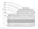
Referring to FIG. 1, the present invention provides a light-emitting device, which comprises: a heat dissipation layer 2, a buffer layer 4 formed on the heat dissipation layer 2, and a light emission unit 6 formed on the buffer layer 4. The heat dissipation layer 2 is made of graphene.
Graphene has thermal conductivity of 4000-6000 W/m·K, which can effectively transfers heat emitting from the light emission unit 6 to the surroundings so as to effectively reduce the temperature of the light-emitting device ad extend the service life of the light-emitting device.
Referring to FIG. 1, in the instant embodiment, the light-emitting device comprises a light-emitting diode (LED) and the light emission unit 6 comprises: an electron transporting layer 62 formed on the buffer layer 4, an emissive layer 64 formed on the electron transporting layer 62, an N type ohmic contact electrode 66 formed on the electron transporting layer 62 and located at one side of the emissive layer 64, a hole transporting layer 67 formed on the emissive layer 64, a transparent conductive layer 68 formed on the hole transporting layer 67, and a P type ohmic contact electrode 69 formed on the transparent conductive layer 68.
In the instant embodiment, the emissive layer 64 is a quantum dot emissive layer, which effectively improves color saturation of the light-emitting diode and enhance color displaying performance of the light-emitting diode.
The transparent conductive layer 68 is an ITO (Indium Tin Oxides) layer.
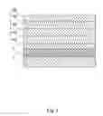
Referring to FIG. 2, in another embodiment, the light-emitting device is an organic electroluminescence display (OLED), which comprises a light emission unit 6′ comprising: an anode 602 formed on a buffer layer 4, a hole transporting layer 604 formed on the anode 602, an organic emissive layer 606 formed on the hole transporting layer 604, an electron transporting layer 608 formed on the organic emissive layer 606, and a cathode 609 formed on the electron transporting layer 608.
Referring to FIG. 3, with additional reference to FIGS. 1 and 2, a manufacturing method of a light-emitting device comprises the following steps:
Step 101: providing a base, wherein the base comprises a heat dissipation layer 2 and the heat dissipation layer 2 is made of graphene.
Graphene has thermal conductivity of 4000-6000 W/m·K, which can effectively transfers heat emitting from the light-emitting device to the surroundings so as to effectively reduce the temperature of the light-emitting device ad extend the service life of the light-emitting device.
Step 102: forming a buffer layer 4 on the heat dissipation layer 2.
Step 103: forming a light emission unit 6 on the buffer layer 4.
In the instant embodiment, the light-emitting device comprises a light-emitting diode (LED) and the light emission unit 6 comprises: an electron transporting layer 62 formed on the buffer layer 4, an emissive layer 64 formed on the electron transporting layer 62, an N type ohmic contact electrode 66 formed on the electron transporting layer 62 and located at one side of the emissive layer 64, a hole transporting layer 67 formed on the emissive layer 64, a transparent conductive layer 68 formed on the hole transporting layer 67, and a P type ohmic contact electrode 69 formed on the transparent conductive layer 68.
The emissive layer 64 is a quantum dot emissive layer, which effectively improves color saturation of the light-emitting diode and enhance color displaying performance of the light-emitting diode. The transparent conductive layer 68 is an ITO (Indium Tin Oxides) layer.
In another embodiment, the light-emitting device is an organic electroluminescence display (OLED), which comprises a light emission unit 6′ comprising: an anode 602 formed on a buffer layer 4, a hole transporting layer 604 formed on the anode 602, an organic emissive layer 606 formed on the hole transporting layer 604, an electron transporting layer 608 formed on the organic emissive layer 606, and a cathode 609 formed on the electron transporting layer 608.
In summary, the present invention provides a light-emitting device and a manufacturing method thereof, in which a heat dissipation layer is made of graphene to effectively dissipate away the heat emitting from the emissive layer so as to effectively reduce the temperature of the light-emitting device and extend the service life of the light-emitting device. Particularly, when the light-emitting device is a light-emitting diode, the emissive layer thereof is a quantum dot emissive layer for effectively improving color saturation of the light-emitting diode and enhancing color displaying performance of the light-emitting diode.
Based on the description given above, those having ordinary skills of the art may easily contemplate various changes and modifications of the technical solution and technical ideas of the present invention and all these changes and modifications are considered within the protection scope of right for the present invention.
Claims
What is claimed is:1. A method for manufacturing a light-emitting device, comprising the following steps:
providing a base, wherein the base comprises a heat dissipation layer made of graphene;
forming a buffer layer on the heat dissipation layer; and
forming a light emission unit on the buffer layer.
2. The method as claimed in claim 1, wherein the light emission unit comprises: an electron transporting layer formed on the buffer layer, an emissive layer formed on the electron transporting layer, an N type ohmic contact electrode formed on the electron transporting layer and located at one side of the emissive layer, a hole transporting layer formed on the emissive layer, a transparent conductive layer formed on the hole transporting layer, and a P type ohmic contact electrode formed on the transparent conductive layer.
3. The method as claimed in claim 2, wherein the emissive layer is a quantum dot emissive layer.
4. The method as claimed in claim 2, wherein the transparent conductive layer is an indium tin oxides layer.
5. The method as claimed in claim 1, wherein the light emission unit comprises: an anode formed on a buffer layer, a hole transporting layer formed on the anode, an organic emissive layer formed on the hole transporting layer, an electron transporting layer formed on the organic emissive layer, and a cathode formed on the electron transporting layer.
6. A method for manufacturing a light-emitting device, comprising the following steps:
providing a base, wherein the base comprises a heat dissipation layer made of graphene;
forming a buffer layer on the heat dissipation layer; and
forming a light emission unit on the buffer layer;
wherein the light emission unit comprises: an electron transporting layer formed on the buffer layer, an emissive layer formed on the electron transporting layer, an N type ohmic contact electrode formed on the electron transporting layer and located at one side of the emissive layer, a hole transporting layer formed on the emissive layer, a transparent conductive layer formed on the hole transporting layer, and a P type ohmic contact electrode formed on the transparent conductive layer.
7. The method as claimed in claim 6, wherein the emissive layer is a quantum dot emissive layer.
8. The method as claimed in claim 6, wherein the transparent conductive layer is an indium tin oxides layer.
Images & Drawings included:


Sources:
- United States Patent and Trademark Office - verify current appl. status at the USPTO↗
Similar patent applications:
- » 20240038955
LIGHT-EMITTING DEVICE, MANUFACTURING METHOD THEREOF, AND LIGHT-EMITTING MODULE - » 20150008455
Molded resin body for surface-mounted light-emitting device, manufacturing method thereof, and surface-mounted light-emitting device - » 20190244939
Chip-on-board display module, manufacturing method thereof, light-emitting diode device and manufacturing method thereof - » 20220375989
Light-emitting device and manufacturing method thereof and manufacturing method of light-emitting apparatus - » 20120112188
Semiconductor light-emitting device, manufacturing method thereof, and lamp - » 20160043148
Pixel structure and manufacturing method thereof, light-emitting device, array substrate and display device - » 20100051981
Semiconductor light-emitting device, manufacturing method thereof, and lamp - » 20070278947
Light-emitting element, manufacturing method thereof, light-emitting device, and electronic device - » 20090008672
LIGHT-EMITTING DEVICE, MANUFACTURING METHOD THEREOF, AND LAMP - » 20050073249
Organic light-emitting device, manufacturing method thereof, and electronic apparatus thereof
Recent applications in this class:
- » 20240395997 2024-11-28
LIGHTING APPARATUS - » 20240154081 2024-05-09
INSULATION SHEET FOR DISPLAY LIGHT SOURCE, AND INSULATION LIGHT SOURCE MODULE, INSULATION BACKLIGHT UNIT, AND DISPLAY DEVICE COMPRISING SAME - » 20240015996 2024-01-11
DISPLAY DEVICE - » 20230387376 2023-11-30
APPARATUS, SYSTEM, AND METHOD FOR ACHIEVING BRIGHTNESS UNIFORMITY ACROSS DISPLAY ELEMENTS - » 20230299254 2023-09-21
DISPLAY DEVICE - » 20230261166 2023-08-17
Method of manufacturing light source device having a bonding layer with bumps and a bonding member - » 20230238500 2023-07-27
DISPLAY DEVICE - » 20230082985 2023-03-16
DISPLAY DEVICE - » 20220320404 2022-10-06
OPTOELECTRONIC SEMICONDUCTOR COMPONENT AND METHOD FOR PRODUCING AN OPTOELECTRONIC SEMICONDUCTOR COMPONENT - » 20220320403 2022-10-06
Semiconductor Component and Method for Producing the Same
Recent applications for this Assignee:
- » 20220052204 2022-02-17
Amorphous silicon thin film transistor and method for manufacturing the same - » 20210405424 2021-12-30
Array substrate - » 20210358953 2021-11-18
Pixel structure, array substrate, and display device - » 20210336040 2021-10-28
Manufacturing method of TFT substrate - » 20210335832 2021-10-28
Thin film transistor (TFT) array substrate and display panel - » 20210191204 2021-06-24
Pixel structure and display panel containing same - » 20210090528 2021-03-25
Display driving system - » 20210083229 2021-03-18
OLED display panel and manufacturing method thereof - » 20210083010 2021-03-18
Color filter substrate having a filter layer disposed on quantum dot layer - » 20210082358 2021-03-18
White balance method and device for LCD panel