Semiconductor device having improved heat dissipation
US20150318376A1
2015-11-05
14/797,573
2015-07-13
✅ Patent granted
US 9,640,632 B2
2017-05-02
-
-
Fernando L Toledo | Adam S Bowen
Withrow & Terranova, P.L.L.C.
2035-07-13
Abstract:
A semiconductor device having improved heat dissipation is disclosed. The semiconductor device includes a semi-insulating substrate and epitaxial layers disposed on the semi-insulating substrate wherein the epitaxial layers include a plurality of heat conductive vias that are disposed through the epitaxial layers with the plurality of heat conductive vias being spaced along a plurality of finger axes that are aligned generally parallel across a surface of the epitaxial layers. The semiconductor device further includes an electrode having a plurality of electrically conductive fingers that are disposed along the plurality of finger axes such that the electrically conductive fingers are in contact with the first plurality of heat conductive vias.
Assignee:
- QORVO US, INC. 1,095 🇺🇸 Greensboro, NC, United States
Applicant:
Interested in similar patents?
Get notified when new applications in this technology area are published.
Classification:
H01L21/76898 » CPC further
Processes or apparatus adapted for the manufacture or treatment of semiconductor or solid state devices or of parts thereof; Manufacture or treatment of devices consisting of a plurality of solid state components formed in or on a common substrate or of parts thereof; Manufacture of integrated circuit devices or of parts thereof; Manufacture of specific parts of devices defined in group; Applying interconnections to be used for carrying current between separate components within a device comprising conductors and dielectrics formed through a semiconductor substrate
H01L23/3677 » CPC further
Details of semiconductor or other solid state devices; Arrangements for cooling, heating, ventilating or temperature compensation ; Temperature sensing arrangements; Selection of materials, or shaping, to facilitate cooling or heating, e.g. heatsinks; Cooling facilitated by shape of device Wire-like or pin-like cooling fins or heat sinks
H01L29/2003 » CPC further
Semiconductor devices adapted for rectifying, amplifying, oscillating or switching, or capacitors or resistors with at least one potential-jump barrier or surface barrier, e.g. PN junction depletion layer or carrier concentration layer; Details of semiconductor bodies or of electrodes thereof; Multistep manufacturing processes therefor; Semiconductor bodies ; Multistep manufacturing processes therefor characterised by the materials of which they are formed including, apart from doping materials or other impurities, only AB compounds Nitride compounds
H01L29/66 IPC
Semiconductor devices adapted for rectifying, amplifying, oscillating or switching, or capacitors or resistors with at least one potential-jump barrier or surface barrier, e.g. PN junction depletion layer or carrier concentration layer; Details of semiconductor bodies or of electrodes thereof; Multistep manufacturing processes therefor Types of semiconductor device ; Multistep manufacturing processes therefor
H01L29/20 IPC
Semiconductor devices adapted for rectifying, amplifying, oscillating or switching, or capacitors or resistors with at least one potential-jump barrier or surface barrier, e.g. PN junction depletion layer or carrier concentration layer; Details of semiconductor bodies or of electrodes thereof; Multistep manufacturing processes therefor; Semiconductor bodies ; Multistep manufacturing processes therefor characterised by the materials of which they are formed including, apart from doping materials or other impurities, only AB compounds
H01L21/283 » CPC further
Processes or apparatus adapted for the manufacture or treatment of semiconductor or solid state devices or of parts thereof; Manufacture or treatment of semiconductor devices or of parts thereof the devices having at least one potential-jump barrier or surface barrier, e.g. PN junction, depletion layer or carrier concentration layer the devices having semiconductor bodies comprising elements of Group IV of the Periodic System or AB compounds with or without impurities, e.g. doping materials; Manufacture of electrodes on semiconductor bodies using processes or apparatus not provided for in groups - Deposition of conductive or insulating materials for electrodes conducting electric current
H01L23/34 » CPC further
Details of semiconductor or other solid state devices Arrangements for cooling, heating, ventilating or temperature compensation ; Temperature sensing arrangements
H01L23/4824 » CPC further
Details of semiconductor or other solid state devices; Arrangements for conducting electric current to or from the solid state body in operation, e.g. leads, terminal arrangements ; Selection of materials therefor consisting of lead-in layers inseparably applied to the semiconductor body Pads with extended contours, e.g. grid structure, branch structure, finger structure
H01L29/66431 » CPC further
Semiconductor devices adapted for rectifying, amplifying, oscillating or switching, or capacitors or resistors with at least one potential-jump barrier or surface barrier, e.g. PN junction depletion layer or carrier concentration layer; Details of semiconductor bodies or of electrodes thereof; Multistep manufacturing processes therefor; Types of semiconductor device ; Multistep manufacturing processes therefor; Multistep manufacturing processes of devices having semiconductor bodies comprising group 14 or group 13/15 materials the devices being controllable only by the electric current supplied or the electric potential applied, to an electrode which does not carry the current to be rectified, amplified or switched, e.g. three-terminal devices; Unipolar field-effect transistors with a heterojunction interface channel or gate, e.g. HFET, HIGFET, SISFET, HJFET, HEMT
H01L29/7786 » CPC further
Semiconductor devices adapted for rectifying, amplifying, oscillating or switching, or capacitors or resistors with at least one potential-jump barrier or surface barrier, e.g. PN junction depletion layer or carrier concentration layer; Details of semiconductor bodies or of electrodes thereof; Multistep manufacturing processes therefor; Types of semiconductor device ; Multistep manufacturing processes therefor controllable by only the electric current supplied, or only the electric potential applied, to an electrode which does not carry the current to be rectified, amplified or switched; Unipolar devices, e.g. field effect transistors; Field effect transistors with two-dimensional charge carrier gas channel, e.g. HEMT ; with two-dimensional charge-carrier layer formed at a heterojunction interface with direct single heterostructure, i.e. with wide bandgap layer formed on top of active layer, e.g. direct single heterostructure MIS-like HEMT
H01L29/0657 » CPC further
Semiconductor devices adapted for rectifying, amplifying, oscillating or switching, or capacitors or resistors with at least one potential-jump barrier or surface barrier, e.g. PN junction depletion layer or carrier concentration layer; Details of semiconductor bodies or of electrodes thereof; Multistep manufacturing processes therefor; Semiconductor bodies ; Multistep manufacturing processes therefor characterised by their shape; characterised by the shapes, relative sizes, or dispositions of the semiconductor regions ; characterised by the concentration or distribution of impurities within semiconductor regions characterised by the shape of the body
H01L29/0696 » CPC further
Semiconductor devices adapted for rectifying, amplifying, oscillating or switching, or capacitors or resistors with at least one potential-jump barrier or surface barrier, e.g. PN junction depletion layer or carrier concentration layer; Details of semiconductor bodies or of electrodes thereof; Multistep manufacturing processes therefor; Semiconductor bodies ; Multistep manufacturing processes therefor characterised by their shape; characterised by the shapes, relative sizes, or dispositions of the semiconductor regions ; characterised by the concentration or distribution of impurities within semiconductor regions characterised by the shape, relative sizes or dispositions of the semiconductor regions or junctions between the regions; Surface layout of cellular field-effect devices, e.g. multicellular DMOS transistors or IGBTs
H01L2924/0002 » CPC further
Indexing scheme for arrangements or methods for connecting or disconnecting semiconductor or solid-state bodies as covered by; Technical content checked by a classifier Not covered by any one of groups , and
H01L21/768 IPC
Processes or apparatus adapted for the manufacture or treatment of semiconductor or solid state devices or of parts thereof; Manufacture or treatment of devices consisting of a plurality of solid state components formed in or on a common substrate or of parts thereof; Manufacture of integrated circuit devices or of parts thereof; Manufacture of specific parts of devices defined in group Applying interconnections to be used for carrying current between separate components within a device comprising conductors and dielectrics
H01L21/02 IPC
Processes or apparatus adapted for the manufacture or treatment of semiconductor or solid state devices or of parts thereof Manufacture or treatment of semiconductor devices or of parts thereof
H01L29/778 IPC
Semiconductor devices adapted for rectifying, amplifying, oscillating or switching, or capacitors or resistors with at least one potential-jump barrier or surface barrier, e.g. PN junction depletion layer or carrier concentration layer; Details of semiconductor bodies or of electrodes thereof; Multistep manufacturing processes therefor; Types of semiconductor device ; Multistep manufacturing processes therefor controllable by only the electric current supplied, or only the electric potential applied, to an electrode which does not carry the current to be rectified, amplified or switched; Unipolar devices, e.g. field effect transistors; Field effect transistors with two-dimensional charge carrier gas channel, e.g. HEMT ; with two-dimensional charge-carrier layer formed at a heterojunction interface
H01L23/367 IPC
Details of semiconductor or other solid state devices; Arrangements for cooling, heating, ventilating or temperature compensation ; Temperature sensing arrangements; Selection of materials, or shaping, to facilitate cooling or heating, e.g. heatsinks Cooling facilitated by shape of device
H01L23/482 IPC
Details of semiconductor or other solid state devices; Arrangements for conducting electric current to or from the solid state body in operation, e.g. leads, terminal arrangements ; Selection of materials therefor consisting of lead-in layers inseparably applied to the semiconductor body
H01L29/06 IPC
Semiconductor devices adapted for rectifying, amplifying, oscillating or switching, or capacitors or resistors with at least one potential-jump barrier or surface barrier, e.g. PN junction depletion layer or carrier concentration layer; Details of semiconductor bodies or of electrodes thereof; Multistep manufacturing processes therefor; Semiconductor bodies ; Multistep manufacturing processes therefor characterised by their shape; characterised by the shapes, relative sizes, or dispositions of the semiconductor regions ; characterised by the concentration or distribution of impurities within semiconductor regions
Description
RELATED APPLICATIONS
This application is a Divisional of U.S. patent application Ser. No. 13/974,488, filed Aug. 23, 2013, which claims the benefit of U.S. provisional patent application number 61/693,076, filed Aug. 24, 2012, the disclosures of which are incorporated herein by reference in their entireties.
FIELD OF THE DISCLOSURE
The present disclosure relates to heat dissipation in semiconductor devices used in power applications.
BACKGROUND
An important property for semiconductor devices used in power applications is thermal resistance, which is a property of a material that is associated with heat conductivity. For example, a material with a high thermal resistance is not a good conductor of heat, whereas a material with a low thermal resistance will conduct heat relatively well. The thermal resistance of certain regions within a semiconductor device will directly determine the maximum heat dissipation of the semiconductor device for a given junction temperature rating. Consequently, it is desirable to minimize the thermal resistance of certain locations within a semiconductor device in order to dissipate heat.
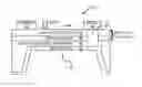
FIG. 1A is a cross-sectional view of a prior art gallium nitride (GaN) high electron mobility transistor (HEMT) 10 depicting a buffer layer 12 between GaN device layers 14 and a semi-insulating substrate 16. The buffer layer 12 and the GaN device layers 14 make up epitaxial layers 18. A source electrode 20, a gate electrode 22 and a drain electrode 24 are disposed onto a surface 26 of the epitaxial layers 18. Heat dissipated in the GaN HEMT 10 must flow through the epitaxial layers 18 to reach the semi-insulating substrate 16, which is selected of a material that provides a relatively low thermal resistivity. For example, the bulk thermal conductivity of GaN is 1.3 W/cm.K compared to a thermal conductivity of around about 3.6 W/cm.K to around about 4.9 W/cm.K for various silicon carbide (SiC) polytypes. Therefore, SiC is a desirable material for the semi-insulating substrate 16. However, due to a lattice mismatch between GaN and common substrates such as SiC, silicon (Si), and Sapphire, a GaN nucleation along with the buffer layer 12 have a high dislocation density, which significantly increases the thermal resistivity of the epitaxial layers 18.
FIG. 1B is a plan view of the prior art GaN HEMT 10 depicting through-wafer vias 28 that are electrically coupled to a bus 30 of the source electrode 20 near the periphery of a die 32. The location of the through-wafer vias 28 prevents the through-wafer vias 28 from efficiently dissipating the heat generated by the GaN HEMT 10 because the largest heat density occurs within a central region of the die 32 in close proximity to drain fingers 34 that are interdigitated with source fingers 36, and gate fingers 38. As a result, there remains a need for a semiconductor device having a structure that dissipates heat with a relatively greater efficiency.
SUMMARY
A semiconductor device having improved heat dissipation is disclosed. The semiconductor device includes a semi-insulating substrate and epitaxial layers disposed on the semi-insulating substrate wherein the epitaxial layers include a plurality of heat conductive vias that are disposed through the epitaxial layers with the plurality of heat conductive vias being spaced along a plurality of finger axes that are aligned generally parallel across a surface of the epitaxial layers. The semiconductor device further includes an electrode having a plurality of electrically conductive fingers that are disposed along the plurality of finger axes such that the electrically conductive fingers are in contact with the first plurality of heat conductive vias. An advantage of the disclosed semiconductor device is that a greater heat density generated within the epitaxial layers is dissipated more efficiently through the plurality of heat conductive vias because they are located where a majority of the heat is generated.
Those skilled in the art will appreciate the scope of the disclosure and realize additional aspects thereof after reading the following detailed description in association with the accompanying drawings.
BRIEF DESCRIPTION OF THE DRAWINGS
The accompanying drawings incorporated in and forming a part of this specification illustrate several aspects of the disclosure, and together with the description serve to explain the principles of the disclosure.
FIG. 1A is a cross-sectional view of a prior art gallium nitride (GaN) high electron mobility transistor (HEMT) depicting a buffer layer between GaN device layers and a semi-insulating substrate.
FIG. 1B is a plan view of the prior art GaN HEMT depicting through-wafer vias electrically coupled to a bus of the source electrode near the edge of a die periphery.
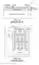
FIG. 2A is a cross-sectional view of an exemplary semiconductor device in the form of a GaN HEMT having heat conductive vias coupled to drain and source electrodes in accordance with the present disclosure.
FIG. 2B is a plan view of the GaN HEMT of FIG. 2A showing pluralities of heat conductive vias in contact with drain and source fingers.
FIG. 3 is a cross-sectional view of an exemplary embodiment of a semiconductor device in the form of a GaN HEMT in which heat conductive vias are further extended into a semi-insulating substrate.
FIG. 4A is a cross-sectional view of an exemplary embodiment of a semiconductor device in the form of a GaN HEMT having through-wafer vias that provide an electrical connection to heat conductive vias.
FIG. 4B is a plan view of the GaN HEMT of FIG. 4A showing a plurality of heat conductive vias in contact with drain fingers and the through-wafer vias.
DETAILED DESCRIPTION
The embodiments set forth below represent the necessary information to enable those skilled in the art to practice the disclosure and illustrate the best mode of practicing the disclosure. Upon reading the following description in light of the accompanying drawings, those skilled in the art will understand the concepts of the disclosure and will recognize applications of these concepts not particularly addressed herein. It should be understood that these concepts and applications fall within the scope of the disclosure and the accompanying claims.
It will be understood that when an element such as a layer, region, or substrate is referred to as being “over,” “on,” “in,” or extending “onto” another element, it can be directly over, directly on, directly in, or extend directly onto the other element or intervening elements may also be present. In contrast, when an element is referred to as being “directly over,” “directly on,” “directly in,” or extending “directly onto” another element, there are no intervening elements present. It will also be understood that when an element is referred to as being “connected” or “coupled” to another element, it can be directly connected or coupled to the other element or intervening elements may be present. In contrast, when an element is referred to as being “directly connected” or “directly coupled” to another element, there are no intervening elements present.
Relative terms such as “below” or “above” or “upper” or “lower” or “horizontal” or “vertical” may be used herein to describe a relationship of one element, layer, or region to another element, layer, or region as illustrated in the Figures. It will be understood that these terms and those discussed above are intended to encompass different orientations of the device in addition to the orientation depicted in the Figures. Moreover, the term high resistivity and the term semi-insulating are used interchangeably throughout the disclosure. Furthermore, the term semi-insulating refers to being electrically insulating.
FIG. 2A is a cross-sectional view of an exemplary semiconductor device 40 in the form of a GaN HEMT with a buffer layer 42 between GaN device layer(s) 44 and a semi-insulating substrate 46. The buffer layer 42 and the GaN device layer(s) 44 make up epitaxial layers 48. A source electrode 50, a gate electrode 52 and a drain electrode 54 are disposed onto a surface 56 of the epitaxial layers 48. FIG. 2A also shows one of a first plurality of heat conductive vias 58 that that are disposed through the epitaxial layers 48 to collectively thermally couple the source electrode 50 to the semi-insulating substrate 46. Similarly, FIG. 2A further shows one of a second plurality of heat conductive vias 60 that are disposed through the epitaxial layers 48 to collectively thermally couple the drain electrode 54 to the semi-insulating substrate 46.
The semi-insulating substrate 46 has a bulk electrical resistivity that ranges from around about 107 ohm-cm to around about 1012 ohm-cm. As a result of this high bulk resistivity range, no significant electrical current flows through the semi-insulating substrate 46 between the source electrode 50 and the drain electrode 54. Suitable materials for the semi-insulating substrate 46 include, but are not limited to high electrical resistivity silicon carbon (SiC), silicon (Si), gallium nitride (GaN), zinc oxide (ZnO), aluminum oxide (Al2O3), and gallium oxide (Ga2O3).
FIG. 2B is a plan view of the semiconductor device 40 of FIG. 2A showing the first plurality of the heat conductive vias 58 being spaced along a first plurality of finger axes 62 that are aligned generally parallel across the surface 56 of the epitaxial layers 48. The source electrode 50 includes a first plurality of electrically conductive fingers 64 that are disposed along the first plurality of finger axes 62 such that the first plurality of electrically conductive fingers 64 are in contact with the first plurality of the heat conductive vias 58. Each of the second plurality of the heat conductive vias 60 are spaced along a second plurality of finger axes 66 that are interdigitated with the first plurality of finger axes 62. The drain electrode 54 includes a second plurality of electrically conductive fingers 68 that are disposed along the second plurality of finger axes 66 such that the second plurality of electrically conductive fingers 68 is in contact with the second plurality of the heat conductive vias 60. Excess heat generated around the first plurality of electrically conductive fingers 64 and the second plurality of electrically conductive fingers 68 is relatively efficiently conducted through the first plurality of the heat conductive vias 58 and the second plurality of the heat conductive vias 60 to the semi-insulating substrate 46 where the excess heat is dissipated.
FIG. 3 is a cross-sectional view of an exemplary embodiment of the semiconductor device 40 in which the first plurality of the heat conductive vias 58 and the second plurality of the heat conductive vias 60 are further extended into a semi-insulating substrate 46. By extending the first plurality of the heat conductive vias 58 and the second plurality of the heat conductive vias 60 into the semi-insulating substrate 46, even greater heat dissipation can be realized.
FIG. 4A is a cross-sectional view of an exemplary semiconductor device 70 in the form of a GaN HEMT with a buffer layer 72 between GaN device layer(s) 74 and a semi-insulating substrate 76. The buffer layer 72 and the GaN device layer(s) 74 make up epitaxial layers 78. A source electrode 80, a gate electrode 82 and a drain electrode 84 are disposed onto a surface 86 of the epitaxial layers 78. FIG. 4A shows one of a plurality of heat conductive vias 88 that are disposed through the epitaxial layers 78 to collectively thermally couple the drain electrode 84 to the semi-insulating substrate 76. In addition, FIG. 4A shows one of a plurality of through hole vias 90 disposed into the semi-insulating substrate 76 to collectively thermally and electrically couple the drain electrode 84 to a back metal 92. Through hole vias 90 are relatively large compared to heat conductive vias 88 therefore direct contact between through hole vias 90 and drain electrode 84 would require relatively wider drain electrodes 84 which would undesirably increase chip size.
FIG. 4B is a plan view of the semiconductor device 70 of FIG. 4A showing the plurality of the heat conductive vias 88 being spaced along a plurality of finger axes 94 that are aligned generally parallel across the surface 86 of the epitaxial layers 78. The drain electrode 84 includes a plurality of electrically conductive fingers 96 that are disposed along the plurality finger axes 94 such that the plurality of electrically conductive fingers 96 are in contact with the plurality of the heat conductive vias 88. In this exemplary embodiment, each of the plurality of heat conductive vias 88 are filled with an electrically conductive material such as metal. Excess heat generated around the plurality of electrically conductive fingers 96 is relatively efficiently conducted through the plurality of the heat conductive vias 88 to the semi-insulating substrate 76 and the back metal 92 where the excess heat is dissipated. While FIGS. 4A and 4B only show the drain being electrically and thermally coupled to the back metal 92 it is to be understood that the drain and/or source can be routed to the back metal 92 to improve thermal and/or electrical performance while reducing die area by eliminating a need for bond pads (not shown) on the front side of a die.
Those skilled in the art will recognize improvements and modifications to the embodiments of the present disclosure. All such improvements and modifications are considered within the scope of the concepts disclosed herein and the claims that follow.
Claims
What is claimed is:1. A method of fabricating a semiconductor device having improved heat dissipation comprising:
providing a semi-insulating substrate;
disposing epitaxial layers on the semi-insulating substrate;
disposing a plurality of heat conductive vias through the epitaxial layers with the plurality of heat conductive vias being spaced along a plurality of finger axes that are aligned generally parallel across a surface of the epitaxial layers; and
disposing an electrode with a plurality of electrically conductive fingers along the plurality of finger axes such that the plurality of electrically conductive fingers are in contact with the plurality of heat conductive vias.
2. The method of claim 1 wherein the plurality of heat conductive vias extend into the semi-insulating substrate.
3. The method of claim 1 further including disposing a second plurality of heat conductive vias through the epitaxial layers with the second plurality of heat conductive vias being spaced along a second plurality of finger axes that are interdigitated with the plurality of finger axes, and disposing a second electrode with a second plurality of electrically conductive fingers along the second plurality of finger axes such that the second plurality of electrically conductive fingers are in contact with the second plurality of heat conductive vias.
4. The method of claim 1 further including extending the plurality of heat conductive vias into the semi-insulating substrate.
5. The method of claim 1 further including filling the plurality of heat conductive vias with an electrically conductive material.
6. The method of claim 5 further disposing a through-hole via into the semi-insulating substrate to electrically couple and thermally couple the plurality of heat conductive vias to a back metal.
7. The method of claim 1 wherein the semi-insulating substrate is made of silicon carbide (SiC) polytypes.
8. The method of claim 7 wherein the SiC polytypes have a bulk thermal conductivity that ranges from around about 3.6 W/cm.K to around about 4.9 W/cm.K.
9. The method of claim 1 wherein a bulk electrical resistivity of the semi-insulating substrate ranges from around about 107 ohm-cm to around about 1012 ohm-cm.
10. The method of claim 9 further including selecting material for making up the semi-insulating substrate from at least one member of the group consisting of SiC, silicon (Si), GaN, zinc oxide (ZnO), aluminum oxide (Al2O3), and gallium oxide (Ga2O3).
11. The method of claim 1 wherein the semiconductor device is a GaN HEMT.
Images & Drawings included:


Sources:
- United States Patent and Trademark Office - verify current appl. status at the USPTO↗
Similar patent applications:
- » 10772252
Semiconductor device with improved heat dissipation, and a method of making semiconductor device - » 20060019430
Semiconductor device with improved heat dissipation, and a method of making semiconductor device - » 20060068522
Semiconductor device with improved heat dissipation, and a method of making semiconductor device - » 20060113647
Semiconductor device with improved heat dissipation - » 20080036073
Semiconductor device and method for manufacturing a semiconductor device having improved heat dissipation capabilities - » 20070117272
Method of making a semiconductor device with improved heat dissipation - » 20080036057
Semiconductor device having improved heat dissipation capabilities - » 10290959
Low profile semiconductor device having improved heat dissipation - » 10217089
Semiconductor devices with improved heat dissipation and method for fabricating same - » 20080296773
Power semiconductor device with improved heat dissipation
Recent applications in this class:
- » 20250072026 2025-02-27
HEMT WITH STAIR-LIKE COMPOUND LAYER AT DRAIN - » 20250072025 2025-02-27
HIGH ELECTRON MOBILITY TRANSISTOR AND METHOD FOR MANUFACTURING THE SAME - » 20250072024 2025-02-27
TRANSISTOR WITH THERMAL PLUG - » 20250040164 2025-01-30
METHOD FOR MANUFACTURING AN OHMIC CONTACT FOR A HEMT DEVICE - » 20250040163 2025-01-30
MANUFACTURING PROCESS OF A SEMICONDUCTOR ELECTRONIC DEVICE INTEGRATING DIFFERENT ELECTRONIC COMPONENTS AND SEMICONDUCTOR ELECTRONIC DEVICE - » 20250031398 2025-01-23
GAN-BASED HEMT STRUCTURE HAVING MULTI-THRESHOLD VOLTAGE, AND PREPARATION METHOD AND APPLICATION THEREFOR - » 20240429306 2024-12-26
SEMICONDUCTOR HETEROSTRUCTURES WITH QUATERNARY III-NITRIDE ALLOY - » 20240371969 2024-11-07
SEMICONDUCTOR DEVICE STRUCTURES AND METHODS OF MANUFACTURING THE SAME - » 20240371968 2024-11-07
HIGH ELECTRON MOBILITY TRANSISTOR - » 20240355902 2024-10-24
CARRIER STRUCTURE FOR ETCH-BACK SILICON-ON-INSULATOR PROCESS
Recent applications for this Assignee:
- » 20240412935 2024-12-12
MEMS SWITCH WITH BEAM CONTACT PORTION CONTINUOUSLY EXTENDING BETWEEN INPUT AND OUTPUT TERMINAL ELECTRODES - » 20240333158 2024-10-03
EFFICIENCY IMPROVEMENT IN A POWER MANAGEMENT INTEGRATED CIRCUIT - » 20240267022 2024-08-08
TOP ELECTRODES AND DIELECTRIC SPACER LAYERS FOR BULK ACOUSTIC WAVE RESONATORS - » 20240258982 2024-08-01
METHOD FOR MANUFACTURING ACOUSTIC DEVICES WITH IMPROVED PERFORMANCE - » 20240250041 2024-07-25
Electronic component with lid to manage radiation feedback - » 20240235513 2024-07-11
Methods and structures for generating smooth electrodes and electrode structures with a uniformly smooth surface - » 20240223129 2024-07-04
Systems and methods for providing an envelope tracking supply voltage - » 20240195391 2024-06-13
CONSOLIDATED ACOUSTIC TRANSFORMER IN TRANSMISSION CHAIN - » 20240178096 2024-05-30
SYSTEM IN PACKAGE WITH FLIP CHIP DIE OVER MULTI-LAYER HEATSINK STANCHION - » 20240173813 2024-05-30
Methods for thinning substrates for semiconductor devices