Low color shift display panel
US20160049124A1
2016-02-18
14/799,831
2015-07-15
✅ Patent granted
US 10,395,607 B2
2019-08-27
-
-
Brian M Butcher
Bacon&Thomas, PLLC
2037-11-17
Abstract:
A low color shift display panel includes a pixel array. The pixel array includes a first sub-pixel and a second sub-pixel. Each of the first sub-pixel and second sub-pixel respectively includes a data line, a gate line, a first transistor coupled to the data line and a first liquid crystal capacitor, a second transistor coupled to the data line and a second liquid crystal capacitor, and a third transistor coupled to a common voltage and the second transistor. The first sub-pixel has a first ratio which is the width-to-length ratio of the third transistor divided by the width-to-length ratio of the second transistor. The second sub-pixel has a second ratio which is the width-to-length ratio of the third transistor divided by the width-to-length ratio of the second transistor. The second ratio is smaller than the first ratio.
Assignee:
- InnoLux Corporation 2,163 🇹🇼 Miao-Li County, Taiwan
Applicant:
Interested in similar patents?
Get notified when new applications in this technology area are published.
Classification:
G09G3/3674 » CPC further
Control arrangements or circuits, of interest only in connection with visual indicators other than cathode-ray tubes for presentation of an assembly of a number of characters, e.g. a page, by composing the assembly by combination of individual elements arranged in a matrix no fixed position being assigned to or needed to be assigned to the individual characters or partial characters by control of light from an independent source using liquid crystals; Control of matrices with row and column drivers Details of drivers for scan electrodes
G09G3/3685 » CPC further
Control arrangements or circuits, of interest only in connection with visual indicators other than cathode-ray tubes for presentation of an assembly of a number of characters, e.g. a page, by composing the assembly by combination of individual elements arranged in a matrix no fixed position being assigned to or needed to be assigned to the individual characters or partial characters by control of light from an independent source using liquid crystals; Control of matrices with row and column drivers Details of drivers for data electrodes
G09G3/3696 » CPC further
Control arrangements or circuits, of interest only in connection with visual indicators other than cathode-ray tubes for presentation of an assembly of a number of characters, e.g. a page, by composing the assembly by combination of individual elements arranged in a matrix no fixed position being assigned to or needed to be assigned to the individual characters or partial characters by control of light from an independent source using liquid crystals; Control of matrices with row and column drivers Generation of voltages supplied to electrode drivers
G09G3/007 » CPC further
Control arrangements or circuits, of interest only in connection with visual indicators other than cathode-ray tubes Use of pixel shift techniques, e.g. by mechanical shift of the physical pixels or by optical shift of the perceived pixels
G09G2300/0443 » CPC further
Aspects of the constitution of display devices; Structural and physical details of display devices; Pixel structures with several sub-pixels for the same colour in a pixel, not specifically used to display gradations
G09G2300/0452 » CPC further
Aspects of the constitution of display devices; Structural and physical details of display devices; Pixel structures Details of colour pixel setup, e.g. pixel composed of a red, a blue and two green components
G09G2300/0456 » CPC further
Aspects of the constitution of display devices; Structural and physical details of display devices; Pixel structures with a reflective area and a transmissive area combined in one pixel, such as in transflectance pixels
G09G2300/0478 » CPC further
Aspects of the constitution of display devices; Structural and physical details of display devices; Details of the physics of pixel operation related to liquid crystal pixels
G09G2310/0216 » CPC further
Command of the display device; Addressing, scanning or driving the display screen or processing steps related thereto; Addressing of scan or signal lines Interleaved control phases for different scan lines in the same sub-field, e.g. initialization, addressing and sustaining in plasma displays that are not simultaneous for all scan lines
G09G2320/02 » CPC further
Control of display operating conditions Improving the quality of display appearance
G09G3/00 IPC
Control arrangements or circuits, of interest only in connection with visual indicators other than cathode-ray tubes
G09G3/3607 » CPC main
Control arrangements or circuits, of interest only in connection with visual indicators other than cathode-ray tubes for presentation of an assembly of a number of characters, e.g. a page, by composing the assembly by combination of individual elements arranged in a matrix no fixed position being assigned to or needed to be assigned to the individual characters or partial characters by control of light from an independent source using liquid crystals for displaying colours or for displaying grey scales with a specific pixel layout, e.g. using sub-pixels
G09G3/36 IPC
Control arrangements or circuits, of interest only in connection with visual indicators other than cathode-ray tubes for presentation of an assembly of a number of characters, e.g. a page, by composing the assembly by combination of individual elements arranged in a matrix no fixed position being assigned to or needed to be assigned to the individual characters or partial characters by control of light from an independent source using liquid crystals
G09G3/3648 » CPC further
Control arrangements or circuits, of interest only in connection with visual indicators other than cathode-ray tubes for presentation of an assembly of a number of characters, e.g. a page, by composing the assembly by combination of individual elements arranged in a matrix no fixed position being assigned to or needed to be assigned to the individual characters or partial characters by control of light from an independent source using liquid crystals; Control of matrices with row and column drivers using an active matrix
G09G2300/0426 » CPC further
Aspects of the constitution of display devices; Structural and physical details of display devices; Structural details of the set of electrodes Layout of electrodes and connections
G09G2300/0447 » CPC further
Aspects of the constitution of display devices; Structural and physical details of display devices; Pixel structures with several sub-pixels for the same colour in a pixel, not specifically used to display gradations for multi-domain technique to improve the viewing angle in a liquid crystal display, such as multi-vertical alignment [MVA]
G09G2300/0814 » CPC further
Aspects of the constitution of display devices; Active matrix structure, i.e. with use of active elements, inclusive of non-linear two terminal elements, in the pixels together with light emitting or modulating elements; Several active elements per pixel in active matrix panels used for selection purposes, e.g. logical AND for partial update
G09G2300/0842 » CPC further
Aspects of the constitution of display devices; Active matrix structure, i.e. with use of active elements, inclusive of non-linear two terminal elements, in the pixels together with light emitting or modulating elements; Several active elements per pixel in active matrix panels forming a memory circuit, e.g. a dynamic memory with one capacitor
G09G2320/0242 » CPC further
Control of display operating conditions; Improving the quality of display appearance Compensation of deficiencies in the appearance of colours
G09G2320/068 » CPC further
Control of display operating conditions; Adjustment of display parameters for control of viewing angle adjustment
G09G2320/0666 » CPC further
Control of display operating conditions; Adjustment of display parameters for control of colour parameters, e.g. colour temperature
G09G2320/0673 » CPC further
Control of display operating conditions; Adjustment of display parameters for control of gamma adjustment, e.g. selecting another gamma curve
Description
BACKGROUND OF THE INVENTION
1. Field of the Invention
The present invention relates to a display panel and, more particularly, to a low color shift display panel.
2. Description of Related Art
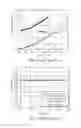
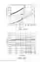
Generally, the side view of the display image may have the phenomenon of color difference and color shift, which is resulted from different optical RGB retardation. In order to solve the phenomenon of color difference and color shift, each sub-pixel, such as the green sub-pixel, the blue sub-pixel, and the red sub-pixel, in the pixel array of a display panel in current design is typically provided with several transistors, and a channel design value, i.e. a width-to-length (W/L) ratio, for the transistor in each sub-pixel is identical, which would affect the color shift performance of the display panel. With reference to FIGS. 1(A) and 1(B), there are shown first and second measurement diagrams for a prior display panel including green sub-pixels, blue sub-pixels, and red sub-pixels, wherein the channel design value (W/L ratio) of the transistor in each sub-pixel is identical. As shown in the dashed box 11 of FIG. 1(A) illustrating a diagram of 64-128 gray levels vs. side view gamma, it can be seen that the green sub-pixel, the blue sub-pixel, and the red sub-pixel are in a divergence state. As shown in FIG. 1(B) illustrating a diagram of chromaticity vs. gray levels, by comparing the normal view of white color coordinate (Wx, Wy) with the side view thereof, it can be seen a significant difference in chromaticity between normal view and side view. When watching the gamma curves in side view, it is found that the red gamma curve is higher than the green gamma curve, the green gamma curve is higher than the blue curve and, when being converted into gray levels, there is a divergence in the 64-128 gray levels, resulting in an undesired yellowish effect.
Therefore, it is desirable to provide a low color shift display panel for effectively preventing color difference and color shift from affecting the image quality.
SUMMARY OF THE INVENTION
The object of the present invention is to provide a low color shift display panel, with which, when watching from one side of the panel, the same effect of being able to avoid color difference and color shift as watching from the front can be obtained.
To achieve the object, there is provided a display panel, which comprises: a pixel array including at least a first sub-pixel and a second sub-pixel. Each of the first sub-pixel and the second sub-pixel respectively includes: a data line; a gate line; a first transistor coupled between the data line and a first liquid crystal capacitor and having a gate coupled to the gate line; a second transistor coupled between the data line and a second liquid crystal capacitor and having a gate coupled to the gate line; and a third transistor coupled between a common voltage and the second transistor and having a gate coupled to the gate line, wherein the first sub-pixel has a first ratio, which is the width-to-length ratio of the third transistor divided by the width-to-length ratio of the second transistor in the first sub-pixel, wherein the second sub-pixel has a second ratio, which is the width-to-length ratio of the third transistor divided by the width-to-length ratio of the second transistor in the second sub-pixel, and wherein the second ratio is smaller than the first ratio.
Therefore, the low color shift display panel according to the present invention is capable of reducing color difference and color shift by adjusting the width-to-length ratios of the transistors, so that watching the display image in side view is as same as watching in normal view.
BRIEF DESCRIPTION OF THE DRAWINGS
FIG. 1(A) schematically illustrates a first measurement diagram of a prior display panel;
FIG. 1(B) schematically illustrates a second measurement diagram of a prior display panel;
FIG. 2 is a schematic diagram of a display panel according to the present invention;
FIG. 3 is a schematic diagram of a pixel array according to the present invention;
FIG. 4(A) schematically illustrates a first measurement diagram of a display panel according to the present invention; and
FIG. 4(B) schematically illustrates a second measurement diagram of a display panel according to the present invention.
DETAILED DESCRIPTION OF THE PREFERRED EMBODIMENT
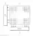
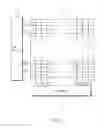
With reference to FIGS. 2 and 3, there are shown schematic diagrams of a display panel and a pixel array according to the present invention. As shown in the figures, the display panel 13 includes: a pixel array 1; a gate driver 14 for connecting a plurality of gate lines G1-Gn of the pixel array 1; a data driver 15 for connecting a plurality of data lines D1-Dn of the pixel array 1. The pixel array 1 includes a first sub-pixel 2, a second sub-pixel 3, and a third sub-pixel 4. Each of the first sub-pixel 2, the second sub-pixel 3, and the third sub-pixel 4 includes: a data line 5; a gate line Gi; a first transistor 8 coupled between the data line 5 and a first liquid crystal capacitor 6 and having a gate coupled to the gate line Gi; a second transistor 9 coupled between the data line 5 and a second liquid crystal capacitor 7 and having a gate coupled to the gate line Gi; and a third transistor 10 coupled between a common voltage Vcom and the second transistor 7 and having a gate coupled to the gate line Gi. That is, the first sub-pixel 2 is connected to the data line Dj+1, the second sub-pixel 3 is connected to the data line Dj+2, and the third sub-pixel 4 is connected to the data line Dj. Preferably, in this embodiment, the first sub-pixel 2 is a green (G) sub-pixel, the second sub-pixel 3 is a blue (B) sub-pixel, and the third sub-pixel 4 is a red (R) sub-pixel, such that the first sub-pixel 2, the second sub-pixel 3, and the third sub-pixel 4 form a complete pixel of a typical liquid crystal display.
The first sub-pixel 2 has a first ratio, which is a value of the width-to-length ratio of the third transistor 10 divided by the width-to-length ratio of the second transistor 9 in the first sub-pixel 2. That is, the first ratio is (W3/L3)/(W2/L2), where W3 and L3 are the channel width and the channel length of the third transistor 10 and W2 and L2 are the channel width and the channel length of the second transistor 9 in the first sub-pixel 2. The second sub-pixel 3 has a second ratio, which is a value of the width-to-length ratio of the third transistor 10 divided by the width-to-length ratio of the second transistor 9 in the second sub-pixel 3. That is, the second ratio is (W3/L3)/(W2/L2), where W3 and L3 are the channel width and the channel length of the third transistor 10 and W2 and L2 are the channel width and the channel length of the second transistor 9 in the second sub-pixel 3. The third sub-pixel 4 has a third ratio, which is a value of the width-to-length ratio of the third transistor 10 divided by the width-to-length ratio of the second transistor 9 in the third sub-pixel 4. That is, the third ratio is (W3/L3)/(W2/L2), where W3 and L3 are the channel width and the channel length of the third transistor 10 and W2 and L2 are the channel width and the channel length of the second transistor 9 in the third sub-pixel 4. In the low color shift display panel of the present invention, the second ratio is smaller than the first ratio and the third ratio is larger than the first ratio. By setting the first ratio, the second ratio, and the third ratio, it is able to adjust the side view performance of the display panel.
In this embodiment, the first ratio is between 0.1 and 0.5, the second ratio is larger than 0.8 times the first ratio, and the third ratio is smaller than 1.2 times the first ratio.
In another embodiment, the first ratio is between 0.2 and 0.4. Preferably, the first ratio is 0.3.
In another embodiment, the second ratio is larger than or equal to 0.9 times the first ratio. Preferably, the second ratio is 0.9 times the first ratio.
In another embodiment, the third ratio is smaller than or equal to 1.1 times the first ratio. Preferably, the third ratio is 1.1 times the first ratio.
FIGS. 4(A) and 4(B) schematically illustrate first and second measurement diagrams of a display panel, respectively, according to the present invention, wherein the second ratio is 0.9 times the first ratio and the third ratio is 1.1 times the first ratio, so that a proportion among the first ratio, the second ratio, and the third ratio is 1:0.9:1.1. As shown in a dashed box 12 of 64-128 gray-level vs. side-view gamma diagram of FIG. 4(A), it is seen that the first (G) sub-pixel 2, the second (B) sub-pixel 3, and the third (R) sub-pixel 4 are in a convergence state. As shown in the chromaticity vs. gray-level diagram of FIG. 4(B), by comparing the white color coordinate (Wx, Wy) of normal view with that of side view, it can be seen that the difference between normal view and side view is getting smaller in chromaticity, so as to reduce the effect of color difference and color shift.
With the low color shift display panel 13 of the present invention, due to that the ratio of each sub-pixel has been properly adjusted, the color difference and color shift can be avoided when watching the display panel in side view, so as to further avoid affecting the image quality and dramatically improve the display quality.
Although the present invention has been explained in relation to its preferred embodiment, it is to be understood that many other possible modifications and variations can be made without departing from the spirit and scope of the invention as hereinafter claimed.
Claims
What is claimed is:1. A display panel, comprising:
a pixel array including at least a first sub-pixel and a second sub-pixel;
wherein each of the first sub-pixel and the second sub-pixel respectively including:
a data line;
a gate line;
a first transistor coupled between the data line and a first liquid crystal capacitor and having a gate coupled to the gate line;
a second transistor coupled between the data line and a second liquid crystal capacitor and having a gate coupled to the gate line; and
a third transistor coupled between a common voltage and the second transistor and having a gate coupled to the gate line,
wherein the first sub-pixel has a first ratio, which is a width-to-length ratio of the third transistor divided by a width-to-length ratio of the second transistor in the first sub-pixel,
wherein the second sub-pixel has a second ratio, which is a width-to-length ratio of the third transistor divided by a width-to-length ratio of the second transistor in the second sub-pixel, and
wherein the second ratio is smaller than the first ratio.
2. The display panel of claim 1, wherein the second ratio is larger than 0.8 times the first ratio.
3. The display panel of claim 1, wherein the second ratio is larger than 0.9 times the first ratio.
4. The display panel of claim 1, wherein the first sub-pixel is a green sub-pixel, and the second sub-pixel is a blue sub-pixel.
5. The display panel of claim 1, wherein the pixel array further includes a third sub-pixel, and the third sub-pixel includes:
a data line;
a gate line;
a first transistor coupled between the data line and a first liquid crystal capacitor and having a gate coupled to the gate line;
a second transistor coupled between the data line and a second liquid crystal capacitor and having a gate coupled to the gate line; and
a third transistor coupled between a common voltage and the second transistor and having a gate coupled to the gate line,
wherein the third sub-pixel has a third ratio, which is a width-to-length ratio of the third transistor divided by a width-to-length ratio of the second transistor in the third sub-pixel, and
wherein the third ratio is larger than the first ratio.
6. The display panel of claim 5, wherein the third ratio is smaller than 1.2 times the first ratio.
7. The display panel of claim 5, wherein the third ratio is smaller than 1.1 times the first ratio.
8. The display panel of claim 5, wherein the third sub-pixel is a red sub-pixel.
9. The display panel of claim 1, wherein the first ratio is between 0.1 and 0.5.
10. The display panel of claim 1, wherein the first ratio is between 0.2 and 0.4.
Images & Drawings included:
Sources:
- United States Patent and Trademark Office - verify current appl. status at the USPTO↗
Similar patent applications:
Recent applications in this class:
- » 20250285601 2025-09-11
DISPLAY SYSTEM - » 20250246164 2025-07-31
ARRAY SUBSTRATE, SHIFT REGISTER UNIT AND DISPLAY APPARATUS - » 20250246163 2025-07-31
ENHANCED COLOR GAMUT PERFORMANCE OF A LIQUID CRYSTAL DISPLAY - » 20250232740 2025-07-17
DISPLAY DEVICE - » 20250232739 2025-07-17
DISPLAY DEVICE - » 20250225945 2025-07-10
DISPLAY PANEL AND DISPLAY APPARATUS - » 20250210004 2025-06-26
APPARATUS FOR COMPENSATING VIEWING ANGLE OF DISPLAY DEVICE AND METHOD THEREOF - » 20250210003 2025-06-26
DISPLAY DEVICE AND ELECTRONIC DEVICE - » 20250118272 2025-04-10
LIQUID CRYSTAL DISPLAY PANEL AND COMPENSATION METHOD THEREOF - » 20250104663 2025-03-27
DISPLAY SUBSTRATE AND DISPLAY DEVICE
Recent applications for this Assignee:
- » 20250291213 2025-09-18
ELECTRONIC DEVICE - » 20250287733 2025-09-11
DISPLAY DEVICE - » 20250285598 2025-09-11
ELECTRONIC DEVICE - » 20250285582 2025-09-11
DISPLAY DEVICE - » 20250285571 2025-09-11
DISPLAY DEVICE - » 20250277973 2025-09-04
TRANSPORTATION APPARATUS - » 20250271964 2025-08-28
ELECTRONIC DEVICE - » 20250261513 2025-08-14
DISPLAY DEVICE - » 20250258383 2025-08-14
ELECTRONIC DEVICE - » 20250254994 2025-08-07
ELECTRONIC DEVICE