Compound semiconductor single crystal ingot for photoelectric conversion devices, photoelectric conversion device, and production method for compound semiconductor single crystal ingot for photoelectric conversion devices
US20160056313A1
2016-02-25
14/780,921
2014-03-11
✅ Patent granted
US 9,362,431 B2
2016-06-07
WO; PCT/JP2014/056230; 20140311
WO; WO2014/156597; 20141002
David Porta | Meenakshi Sahu
Birch, Stewart, Kolasch & Birch, LLP
2034-03-11
Abstract:
The present invention increases the conversion efficiency of a photoelectric conversion element that uses cadmium zinc telluride or cadmium telluride (Cd(Zn)Te) compound semiconductor single crystals containing a group 1A element as an impurity. A heat-resistant pot is filled with raw material and a group 1A element, which is reacted with a portion of the raw material, and the container is heated, thereby melting the raw material into a melt and diffusing the dissociated group 1A element in the melt, producing single crystals from the melt. Compound semiconductor single crystals for photoelectric conversion elements having a hole concentration of 4×1015 cm−3 to 1×1018 cm−3 are produced in this manner. Using a substrate (2) that has been cut out from the compound semiconductor single crystals for photoelectric conversion elements enables the conversion efficiency of a photoelectric conversion element (10) to be increased.
Inventors:
- Ryuichi HIRANO 12 🇯🇵 Tokyo, Japan
- Akira NODA 2 🇯🇵 Kitaibaraki-shi, Ibaraki, Japan
- Ryuichi HIRANO 2 🇯🇵 Chiyoda-ku, Tokyo, Japan
- Akira Noda 10 🇯🇵 Kitaibaraki, Japan
Assignee:
- JX NIPPON MINING & METALS CORPORATION 317 🇯🇵 Tokyo, Japan
- JX NIPPON MINING & METALS CORPORATION 472 🇯🇵 Tokyo, Japan
Applicant:
Interested in similar patents?
Get notified when new applications in this technology area are published.
Classification:
C30B11/002 » CPC further
Single-crystal growth by normal freezing or freezing under temperature gradient, e.g. Bridgman-Stockbarger method Crucibles or containers for supporting the melt
C30B11/00 » CPC further
Single-crystal growth by normal freezing or freezing under temperature gradient, e.g. Bridgman-Stockbarger method
C30B29/48 » CPC further
Single crystals or homogeneous polycrystalline material with defined structure characterised by the material or by their shape; Inorganic compounds or compositions; Sulfur-, selenium- or tellurium-containing compounds AB compounds wherein A is Zn, Cd or Hg, and B is S, Se or Te
C30B11/065 » CPC further
Single-crystal growth by normal freezing or freezing under temperature gradient, e.g. Bridgman-Stockbarger method adding crystallising materials or reactants forming it to the melt at least one but not all components of the crystal composition being added before crystallising, e.g. synthesis
H01L31/0296 IPC
Semiconductor devices sensitive to infra-red radiation, light, electromagnetic radiation of shorter wavelength or corpuscular radiation and specially adapted either for the conversion of the energy of such radiation into electrical energy or for the control of electrical energy by such radiation; Processes or apparatus specially adapted for the manufacture or treatment thereof or of parts thereof; Details thereof characterised by their semiconductor bodies characterised by the material; Inorganic materials including, apart from doping material or other impurities, only AB compounds, e.g. CdS, ZnS, HgCdTe
H01L31/02963 » CPC further
Semiconductor devices sensitive to infra-red radiation, light, electromagnetic radiation of shorter wavelength or corpuscular radiation and specially adapted either for the conversion of the energy of such radiation into electrical energy or for the control of electrical energy by such radiation; Processes or apparatus specially adapted for the manufacture or treatment thereof or of parts thereof; Details thereof characterised by their semiconductor bodies characterised by the material; Inorganic materials including, apart from doping material or other impurities, only AB compounds, e.g. CdS, ZnS, HgCdTe characterised by the doping material
H01L31/02966 » CPC further
Semiconductor devices sensitive to infra-red radiation, light, electromagnetic radiation of shorter wavelength or corpuscular radiation and specially adapted either for the conversion of the energy of such radiation into electrical energy or for the control of electrical energy by such radiation; Processes or apparatus specially adapted for the manufacture or treatment thereof or of parts thereof; Details thereof characterised by their semiconductor bodies characterised by the material; Inorganic materials including, apart from doping material or other impurities, only AB compounds, e.g. CdS, ZnS, HgCdTe including ternary compounds, e.g. HgCdTe
C30B11/06 IPC
Single-crystal growth by normal freezing or freezing under temperature gradient, e.g. Bridgman-Stockbarger method adding crystallising materials or reactants forming it to the melt at least one but not all components of the crystal composition being added
H01L31/036 » CPC main
Semiconductor devices sensitive to infra-red radiation, light, electromagnetic radiation of shorter wavelength or corpuscular radiation and specially adapted either for the conversion of the energy of such radiation into electrical energy or for the control of electrical energy by such radiation; Processes or apparatus specially adapted for the manufacture or treatment thereof or of parts thereof; Details thereof characterised by their semiconductor bodies characterised by their crystalline structure or particular orientation of the crystalline planes
H01L31/04 » CPC further
Semiconductor devices sensitive to infra-red radiation, light, electromagnetic radiation of shorter wavelength or corpuscular radiation and specially adapted either for the conversion of the energy of such radiation into electrical energy or for the control of electrical energy by such radiation; Processes or apparatus specially adapted for the manufacture or treatment thereof or of parts thereof; Details thereof adapted as photovoltaic [PV] conversion devices
H01L31/1832 » CPC further
Semiconductor devices sensitive to infra-red radiation, light, electromagnetic radiation of shorter wavelength or corpuscular radiation and specially adapted either for the conversion of the energy of such radiation into electrical energy or for the control of electrical energy by such radiation; Processes or apparatus specially adapted for the manufacture or treatment thereof or of parts thereof; Details thereof; Processes or apparatus specially adapted for the manufacture or treatment of these devices or of parts thereof the active layers comprising only AB compounds, e.g. CdS, ZnS, CdTe comprising ternary compounds, e.g. Hg Cd Te
H01L31/18 IPC
Semiconductor devices sensitive to infra-red radiation, light, electromagnetic radiation of shorter wavelength or corpuscular radiation and specially adapted either for the conversion of the energy of such radiation into electrical energy or for the control of electrical energy by such radiation; Processes or apparatus specially adapted for the manufacture or treatment thereof or of parts thereof; Details thereof Processes or apparatus specially adapted for the manufacture or treatment of these devices or of parts thereof
Y02E10/543 » CPC further
Energy generation through renewable energy sources; Photovoltaic [PV] energy Solar cells from Group II-VI materials
Y02E10/543 » CPC further
Energy generation through renewable energy sources; Photovoltaic [PV] energy Solar cells from Group II-VI materials
G01T1/20 IPC
Measuring X-radiation, gamma radiation, corpuscular radiation, or cosmic radiation; Measuring radiation intensity with scintillation detectors
H01L31/073 » CPC further
Semiconductor devices sensitive to infra-red radiation, light, electromagnetic radiation of shorter wavelength or corpuscular radiation and specially adapted either for the conversion of the energy of such radiation into electrical energy or for the control of electrical energy by such radiation; Processes or apparatus specially adapted for the manufacture or treatment thereof or of parts thereof; Details thereof adapted as photovoltaic [PV] conversion devices characterised by at least one potential-jump barrier or surface barrier the potential barriers being only of the PN heterojunction type comprising only AB compound semiconductors, e.g. CdS/CdTe solar cells
Description
TECHNICAL FIELD
The present invention relates to a compound semiconductor single crystal used in photoelectric conversion devices of solar cells, a photoelectric conversion device using this compound semiconductor single crystal, and a method for producing this compound semiconductor single crystal.
BACKGROUND ART
Group II-VI compound semiconductors such as cadmium telluride (CdTe) and cadmium zinc telluride (CdZnTe) are known as semiconductor materials for forming substrates of devices for detecting radiation or infrared rays. Crystals of CdTe and CdZnTe (hereafter “Cd(Zn)Te”) containing no impurity (undoped) or containing a group 1A element, such as sodium (Na) or lithium (Li), show p-type electric properties. In other words, a p-type Cd(Zn)Te crystal can be prepared by adding an appropriate amount of impurity, such as Na or Li, to the crystal.
A trace amount of Na or Li, which is contained in the quartz component of a crucible used for producing crystals, intrudes a Cd(Zn)Te crystal during its production process without intentions of manufacturers. The concentrations of these impurities, however, must be reduced in production of the Cd(Zn)Te crystal for a radiation detecting device. Thus, the solidification rate of Cd(Zn)Te has been limited for growing a Cd(Zn)Te crystal, in other words, its crystal growth has been finished before the melt has completely solidified, so as to leave Na and Li in the melt (see Patent document 1).
RELATED ART DOCUMENTS
Patent Documents
- [Patent Document 1] Japanese Patent Application Laid-Open No. 11-228299
- [Patent Document 2] Japanese Patent Application Laid-Open No. 05-347425
- [Patent Document 3] Japanese Patent Application Laid-Open No. 09-074210
- [Patent Document 4] WO2012-114803
SUMMARY OF THE INVENTION
Problems to be Solved by the Invention
The Cd(Zn)Te crystal is also used as substrate materials for cells (photoelectric conversion devices) of solar cells. A photoelectric conversion device including a Cd(Zn)Te crystal has been proposed and developed which has a structure including a p-type semiconductor layer made of a Cd(Zn)Te crystal, an n-type semiconductor layer made of, for example, cadmium sulfide (CdS), a front electrode, and a rear electrode (see Patent documents 2 and 3). Photoelectric conversion devices including substrates made of a Cd(Zn)Te crystal can be produced by a simple manufacturing process at significantly low manufacturing cost compared to devices produced with any other material, such as silicon (Si), and their future market expansion is expected.
The Cd(Zn)Te crystal for photoelectric conversion devices must have a reduced resistivity unlike radiation detecting devices used under high voltage. It is known that the carrier concentration in the crystal should be increased to reduce the resistivity. The increased carrier concentration also leads to improved conversion efficiency. Thus, in the production of a Cd(Zn)Te crystal containing Na or Li for photoelectric conversion devices, the Na or Li concentration in the crystal is increased without control of diffusion of Na or Li to a crucible.
Such addition of Na or Li, however, limits the hole concentration to about 1×1015 cm−3 at most, which causes the conversion efficiency of the photoelectric conversion device to be lowered compared to those prepared with any other semiconductor crystal such as Si.
Polycrystalline CdTe thin films have been produced from powdered CdTe having an acceptor concentration in the range of 1×1017 cm−3 to 1×1018 cm−3 by a close-spaced sublimation (CSS) method (Patent document 4).
This patent document, however, discloses only an example using antimony as an acceptor and thus it is not clear that a desired acceptor concentration can be achieved using Na or Li as an impurity. Furthermore, only a polycrystalline thin film can be produced by this method. Since a large number of grain boundaries are present in the polycrystalline matrix, carriers produced by photoexcitation are readily scattered, which shortens the carrier lifetime. As a result, polycrystalline solar cells cannot have high conversion efficiency compared to monocrystalline cells.
A recent demand is to further improve the conversion efficiency of a photoelectric conversion device of Cd(Zn)Te. At present, however, a method for efficiently incorporating Na or Li to a single crystal has not been developed yet other than utilizing diffusion of Na or Li from a crucible as described in Patent document 1.
An object of the present invention, which has been made to solve the above problems, is to improve the conversion efficiency of a photoelectric conversion device including a compound semiconductor single crystal containing at least one group 1A impurity element.
Means for Solving the Problems
The invention of claim 1 is a compound semiconductor single crystal for a photoelectric conversion device containing at least one group 1A impurity element and having a hole concentration in the range of 4×1015 cm−3 to 1×1018 cm−3.
The invention of claim 2 is the compound semiconductor single crystal for a photoelectric conversion device according to claim 1, wherein the at least one group 1A element is sodium and the concentration of the sodium ranges from 2×1015 cm−3 to 1×1020 cm−3.
The invention of claim 3 is the compound semiconductor single crystal for a photoelectric conversion device according to claim 2, wherein the at least one group 1A element is sodium and lithium and the concentration of the lithium ranges from 2×1015 cm−3 to 1×1020 cm−3.
The invention of claim 4 is the compound semiconductor single crystal for a photoelectric conversion device according to claim 1, wherein the at least one group 1A element is lithium and the concentration of the lithium ranges from 2×1015 cm−3 to 1×1020 cm−3.
The invention of claim 5 is the compound semiconductor single crystal for a photoelectric conversion device according to claim 1, wherein the compound semiconductor is cadmium telluride or cadmium zinc telluride.
The invention of claim 6 is a photoelectric conversion device: including a p-type semiconductor substrate formed by a compound semiconductor single crystal for a photoelectric conversion device according to any one of the claims 1 to 5, an n-type semiconductor layer formed on a first main surface of the p-type semiconductor substrate, a first electrode formed on a surface of the n-type semiconductor layer, and a second electrode formed on a second main surface of the p-type semiconductor substrate.
The invention of claim 7 is a method for producing a compound semiconductor single crystal for a photoelectric conversion device containing at least one group 1A impurity element, the method including: filling a heat-resistant pot (crucible) with a raw material and a group 1A element reacting with part of the raw material, melting the raw material to obtain a melt by heating the pot, and diffusing the dissociated group 1A element into the melt, and growing a single crystal from the melt.
The invention of claim 8 is the method for producing a compound semiconductor single crystal for a photoelectric conversion device according to claim 7, wherein the at least one group 1A element is sodium, and the pot is filled with the raw material and sodium reacting with part of the raw material.
The invention of claim 9 is the method for producing a compound semiconductor single crystal for a photoelectric conversion device according to claim 8, wherein the at least one group 1A element is sodium and lithium, and the pot is filled with the raw material, sodium reacting with part of the raw material, and lithium reacting with part of the raw material.
The invention of claim 10 is the method for producing a compound semiconductor single crystal for a photoelectric conversion device according to claim 7, wherein the at least one group 1A element is lithium, and the pot is filled with the raw material and lithium reacting with part of the raw material.
The invention of claim 11 is the method for producing a compound semiconductor single crystal for a photoelectric conversion device according to any one of claims 7 to 10, wherein the raw materials include tellurium and cadmium or include tellurium, zinc, and cadmium, and the pot is filled with the raw materials and a group 1A element reacting with the tellurium.
The invention of claim 12 is the method for producing a compound semiconductor single crystal for a photoelectric conversion device according to claim 7, wherein the pot is composed of boron nitride.
The invention of claim 13 is the method for producing a compound semiconductor single crystal for a photoelectric conversion device according to claim 7, wherein the pot is composed of quartz.
The invention of claim 14 is the method for producing a compound semiconductor single crystal for a photoelectric conversion device according to claim 7, wherein the melt is solidified by a vertical gradient freeze (VGF) process.
Advantageous Effects of the Invention
According to the present invention, any amount of group 1A element can readily be diffused into a single crystal using a stable group 1A element reacting with part of a raw material. Hence, the hole concentration in a compound semiconductor single crystal for a photoelectric conversion device can be increased to the range of 4×1015 cm−3 to 1×1018 cm−3 which cannot be achieved by any conventional method involving diffusion of impurities from the quartz component.
Accordingly, the conversion efficiency of a photoelectric conversion device including a Cd(Zn)Te single crystal containing at least one group 1A impurity element can be improved.
BRIEF DESCRIPTION OF DRAWINGS
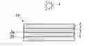
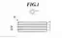
FIG. 1 is a longitudinal sectional view of a photoelectric conversion device according to an embodiment of the present invention.
EMBODIMENTS FOR CARRYING OUT THE INVENTION
First Embodiment
A first embodiment of the present invention will now be described in detail.
[Configuration of Photoelectric Conversion Device]
An overview configuration of a photoelectric conversion device of the present embodiment will be described. FIG. 1 is a schematic longitudinal sectional view of a photoelectric conversion device 10 of the present embodiment. In each layer, the upper surface (the surface facing Sun “S”) is defined as a “front surface” and the lower surface as a “rear surface” in FIG. 1.
The photoelectric conversion device 10 of the present embodiment includes a p-type semiconductor substrate (hereafter “p-type substrate 2”) cut out from a compound semiconductor single crystal for a photoelectric conversion device of the present embodiment, an n-type semiconductor layer (hereafter “n-type layer 3”) formed on the front surface (first main surface 2a) of the p-type substrate 2, a front electrode (first electrode) formed on the front surface of the n-type layer 3, a rear electrode 5 (second electrode) formed on the rear surface (second main surface 2b) of the p-type substrate 2.
The p-type substrate 2 of the present embodiment is a plate made of a single crystal of a group II-VI compound semiconductor, such as cadmium telluride (CdTe) or cadmium zinc telluride (CdZnTe). The CdTe or CdZnTe single crystal contains a group 1A element, specifically sodium (Na) or lithium (Li), as a dopant (impurity), and has a hole concentration in the range of 4×1015 cm−3 to 1×1018 cm−3. Hereafter, both CdTe and CdZnTe are collectively referred to as Cd(Zn)Te unless their distinction is necessary.
The n-type layer 3 is a thin film made of a single crystal of, for example, cadmium sulfide (hereafter “CdS”).
The front electrode 4 is a thin film made of a transparent conductive material of, for example, indium tin oxide (ITO).
The rear electrode 5 is, for example, a graphite plate.
[Method for Producing Compound Semiconductor Crystal for Photoelectric Conversion Device]
A method for producing a Cd(Zn)Te single crystal 1 will be described. This method involves preparatory, heating, and single crystal growing steps.
In the preparatory step, a quartz crucible (hereafter merely “crucible”), which is a heat-resistant pot, is filled with raw materials (Cd and Te or Cd, Te, and Zn) for the Cd(Zn)Te single crystal and further sodium telluride (Na2Te) or lithium telluride (Li2Te). Na in Na2Te or Li in Li2Te will function as a dopant in the Cd(Zn)Te single crystal later. Although the surface of elemental Na reacts with oxygen to be oxidized, the oxidation of Na and Li can be prevented by filling them as a telluride of Na or Li (one reacting with part of the raw materials). In particular, elemental Li is difficult to handle because it highly reacts with oxygen, but this method can make this filling operation safe. This crucible is then placed in a quartz ampule (hereafter “ampule”). After that, the inside of the ampule is evacuated, and the opening of the quartz ampule is melt-sealed. The ampule is then placed in a single crystal growing furnace.
After the placement of the ampule, the process proceeds to the heating step. In this step, the ampule is heated to melt the raw materials. In the present embodiment, the Cd(Zn)Te single crystal is grown by a VGF method in a VGF furnace as a single crystal growing furnace. After the placement of the ampule and the seal of the VGF furnace, the temperature in the VGF furnace is increased to melt the raw materials, Cd and Te or Cd, Te, and Zn, into the Cd(Zn)Te melt (hereafter “melt”). Na2Te or Li2Te filled in the crucible, then, dissociates, and Na or Li diffuses into the melt. Na or Li contained in the quartz component of the crucible also diffuses into the melt.
After Na or Li is sufficiently diffused into melt, the process proceeds to the single crystal growing step. In this step, a heater in the VGF furnace is adjusted such that the temperatures is low at the upper portion of the crucible placed in the furnace and high at the lower portion thereof to form a temperature distribution gradient in the furnace. While the temperature distribution gradient is being formed, the temperature of the melt is gradually lowered to grow the Cd(Zn)Te single crystal downward from the liquid surface of the melt.
An Cd(Zn)Te single crystal ingot (hereafter “ingot”) of the present embodiment containing Na or Li as an impurity is produced through the above-described steps, the ingot having a high hole concentration in the range of 4×1015 cm−3 to 1×1018 cm−3, and is suitable for photoelectric conversion device substrates.
[Production of Photoelectric Conversion Device]
A method for producing the photoelectric conversion device 10 of the present embodiment including the p-type substrate 2 made of the Cd(Zn)Te single crystal will be described. The method for producing the photoelectric conversion device 10 involves a cutting step, a lapping step, a step of forming an n-type layer, a step of forming a front electrode, a step of forming a rear electrode, and a dicing step.
In the cutting step, the both upper and lower ends of the ingot are cut off and the surface of the remaining middle portion (straight body portion) of the ingot is cut into a cylindrical shape. The ingot is then cut perpendicular to the single crystal growth direction (parallel to the circular surfaces at the both ends of the ingot) to cut out a plurality of discoidal Cd(Zn)Te wafers (hereafter “wafer 1”).
After the wafer 1 is cut out, the process proceeds to the lapping step. In this step, the cut section of the wafer 1 is polished with a lapping abrasive to remove the asperities.
After the cutting section is planarized, the process proceeds to the mirror polishing step. In this step, the lapped surface of the wafer 1 is polished with a mirror polishing abrasive to prepare a mirror finished surface.
After the wafer 1 is polished, the process proceeds to the step of forming the n-type layer. In this step, the wafer 1 and the raw materials, Cd and S, for the n-type layer 3 are placed in a vapor phase epitaxy system. A CdS thin film is then epitaxially grown on the surface of the wafer 1. This thin film is grown into the n-type layer 3 with a predetermined thickness.
After the n-type layer 3 is formed, the process proceeds to the step of forming a front electrode. In this step, the front electrode 4 of an ITO thin film is formed on the surface of the n-type layer 3. The electrode may be formed by any conventional process, including physical vapor deposition (PVD), such as sputtering, film deposition, ion-assisted vacuum deposition; and other deposition, such as chemical vapor deposition (CVD), coating, spin-coating, and spraying.
After the front electrode 4 is formed, the process proceeds to the step of forming a rear electrode. In this step, the rear electrode 5 of a graphite thin film is formed on the surface of the wafer 1. The electrode may be formed by any conventional process including coating and vapor deposition.
After the rear electrode 5 is formed, the process proceeds to the dicing step. In this step, the ends of the wafer 1 provided with the n-type layer 3, the front electrode 4, and the rear electrode 5 are formed on the main surfaces 1a or 1b is trimmed into one photoelectric conversion device 10, or the wafer 1 is divided into a plurality of substrates 1, 1. to cut out a plurality of photoelectric conversion devices 10.
The photoelectric conversion device 10 of the present embodiment is produced through the steps described above. Since the photoelectric conversion device 10 has a hole concentration in the range of 4×1015 cm−3 to 1×1018 cm−3, it has a high conversion efficiency compared to conventional devices.
Examples
A CdTe single crystal actually produced by the above-described product ion method will now be described.
A quartz crucible was filled with 3900 g of polycrystalline CdTe raw material and 1 mg of Na2Te, and was placed in an ampule. The ampule was then placed in a VGF furnace to melt the raw material and form a temperature gradient to the melt, so as to grow a single crystal downward from the upper end of the melt.
The observed surface of the produced CdTe single crystal showed no precipitate. The Na and Li concentrations measured in the CdTe single crystal were 1E+16 cm−3 and 2E+15 cm−3 respectively. The results demonstrate that the CdTe single crystal produced according to the present embodiment does not contain excess concentrations of impurities.
The hole concentration in the produced CdTe single crystal measured by a hall measurement apparatus was about 1×1018 cm−3 at most and about 4×1015 cm−3 at least.
As described above, since stable Na or Li reacting with part of Te is used in the present embodiment, any amount of Na or Li can be readily diffused into the single crystal. Thus, the hole concentration in a compound semiconductor crystal for a photoelectric conversion device can be increased to the range of 4×1015 cm−3 to 1×1018 cm−3 which cannot be achieved by any conventional process which involves diffusion of the impurity from its quartz component. In particular, because a quartz crucible is used in the present embodiment, Na and Li also diffuse from its quartz component into the melt while the crucible is being heated. In this way, the hole concentration in the compound semiconductor crystal for a photoelectric conversion device can be further increased.
As a result, the conversion efficiency of the photoelectric conversion device 10 made of Cd(Zn)Te single crystal containing Na and Li as an impurity can be improved.
Second Embodiment
A second embodiment of the present invention will now be described. The description on the same components as those in the first embodiment is omitted.
The second embodiment is different from the first embodiment in that a crucible composed of pBN (pyrolytic boron nitride) is used for filling raw materials.
After the step of filling the crucible with the raw materials and the like to the step of sealing the VGF furnace, the temperature in the VGF furnace is increased to melt the raw materials. Na2Li or Li2Te filled in the crucible then begins to dissociate, and Na or Li diffuses into the melt. Since the pBN crucible is used in the present embodiment, Na or Li does not diffuse from the crucible.
Thus, the second embodiment using the pBN crucible can achieve a high hole concentration in the range of 4×1015 cm−3 to 1×1018 cm−3 in the compound semiconductor crystal for a photoelectric conversion device without diffusion of elements other than Na and Li from the crucible, like the first embodiment.
In particular, since Li has a higher electric activation rate than Na, the hole concentration can be increased with a small amount of Li2Te without precipitation, which occurs at high concentrations of impurities.
Third Embodiment
A third embodiment of the present invention will now be described. The description on the same components as those in the first and second embodiments is omitted.
The third embodiment is different from the first and second embodiments in that both of Na2Li and Li2Te are used as group 1A elements reacting with part of the raw materials, and the material for a crucible for filling the raw materials is not limited.
After the step of filling the crucible with the raw materials to the step of sealing the VGF furnace, the temperature in the VGF furnace is increased to melt the raw materials. Na2Li and Li2Te filled in the crucible then begin to dissociate, and Na and Li diffuse into the melt.
In the third embodiment using both of Na2Li and Li2Te, the hole concentration in the compound semiconductor crystal for a photoelectric conversion device can be more readily increased to the range of 4×1015 cm−3 to 1×1018 cm−3 compared to the first and second embodiments.
Although the invention made by the present inventor has been specifically described based on the embodiments above, the present invention should not be limited to the above-described embodiments, and can be modified without departing from the spirit of the present invention.
For example, the method for producing the CdTe or CdZnTe single crystal is described in the embodiments. The present invention can also be applied to all methods for producing any compound semiconductor crystals for photoelectric conversion devices containing group 1A elements as dopants, including not only polycrystalline CdTe and CdZnTe but also monocrystalline zinc telluride (ZnTe).
In the photoelectric conversion device 10 of the embodiment, the n-type layer 3 of a thin-film is formed on the main surface of a plate made of the Cd(Zn)Te single crystal, but the Cd(Zn)Te thin layer may be formed on a surface made of, for example, a glass, on which the n-type layer 3 may be formed. In this case, the polycrystalline Cd(Zn)Te is produced by the method of the present embodiment, from which a thin film can be formed by, for example, a close-spaced sublimation process.
In the embodiments, ITO is used for the front electrode. Alternatively, any other transparent and conductive material may be employed. Furthermore, the rear electrode may be composed of a metal or any other conductive material in place of graphite.
The embodiments disclosed herein are all for illustration only in all respects and not intended to be limiting. The scope of the present invention should be defined not by the above description but by the appended claims, and all modifications are intended to be included without departing from the meaning and scope equivalent to the claims.
INDUSTRIAL APPLICABILITY
The present invention can applied to the cells of solar batteries, for example.
EXPLANATION OF REFERENCE NUMERALS
- 10: photoelectric conversion device
- 2: p-type semiconductor substrate (compound semiconductor single crystal for a photoelectric conversion device, Cd(Zn)Te single crystal)
- 2a: first main surface
- 2b: second main surface
- 3: n-type semiconductor layer
- 4: front electrode (first electrode)
- 5: rear electrode (second electrode)
Claims
1. A compound semiconductor single crystal ingot of cadmium telluride or cadmium zinc telluride for a photoelectric conversion device containing at least one group 1A impurity element and having a hole concentration in the range of 4×1015 cm−3 to 1×1018 cm−3.
2. The compound semiconductor single crystal ingot for a photoelectric conversion device according to claim 1, wherein the at least one group 1A element comprises sodium and the concentration of the sodium ranges from 2×1015 cm−3 to 1×1020 cm−3.
3. The compound semiconductor single crystal ingot for a photoelectric conversion device according to claim 2, wherein the at least one group 1A element comprises sodium and lithium and the concentration of the lithium ranges from 2×1015 cm−3 to 1×1020 cm−3.
4. The compound semiconductor single crystal ingot for a photoelectric conversion device according to claim 1, wherein the at least one group 1A element is comprises lithium and the concentration of the lithium ranges from 2×1015 cm−3 to 1×1020 cm−3.
5. (canceled)
6. A photoelectric conversion device: comprising
a p-type semiconductor substrate by cut out from a compound semiconductor single crystal ingot for a photoelectric conversion device according to claim 1,
an n-type semiconductor layer formed on a first main surface of the p-type semiconductor substrate,
a first electrode formed on a surface of the n-type semiconductor layer, and
a second electrode formed on a second main surface of the p-type semiconductor substrate.
7. A method for producing a compound semiconductor single crystal ingot of cadmium telluride or cadmium zinc telluride for a photoelectric conversion device containing at least one group 1A impurity element, the method comprising:
filling a heat-resistant pot with a raw material and a group 1A element combined with part of the raw material,
melting the raw material to obtain a melt by heating the pot, and diffusing the dissociated group 1 A element into the melt, and
growing a single crystal having a hole concentration in the range of 4×1015 cm−3 to 1×1018 cm−3 from the melt.
8. The method for producing a compound semiconductor single crystal ingot for a photoelectric conversion device according to claim 7, wherein
the at least one group 1A element is sodium, and
the pot is filled with the raw material and sodium telluride.
9. The method for producing a compound semiconductor single crystal ingot for a photoelectric conversion device according to claim 8, wherein
the at least one group 1A element is sodium and lithium, and
the pot is filled with the raw material, sodium telluride, and lithium telluride.
10. The method for producing a compound semiconductor single crystal ingot for a photoelectric conversion device according to claim 7, wherein
the at least one group 1A element is lithium, and
the pot is filled with the raw material and lithium telluride.
11. (canceled)
12. The method for producing a compound semiconductor single crystal ingot for a photoelectric conversion device according to claim 7, wherein the pot is composed of boron nitride.
13. The method for producing a compound semiconductor single crystal ingot for a photoelectric conversion device according to claim 7, wherein the pot is composed of quartz.
14. The method for producing a compound semiconductor single crystal ingot for a photoelectric conversion device according to claim 7, wherein the melt is solidified by a vertical gradient freeze process.
Images & Drawings included:
Sources:
- United States Patent and Trademark Office - verify current appl. status at the USPTO↗
Recent applications in this class:
- » 20230275164 2023-08-31
Image Sensor and Method for Forming the Same - » 20230197869 2023-06-22
OPTOELECTRONIC DEVICE - » 20220393048 2022-12-08
OPTOELECTRONIC DEVICE - » 20210020798 2021-01-21
Power photodiode structures, methods of making, and methods of use - » 20200365748 2020-11-19
Optoelectronic device - » 20180315870 2018-11-01
Optoelectronic device - » 20160268459 2016-09-15
Photoelectric conversion element, photoelectric conversion module, and solar photovoltaic power generation system - » 20160268458 2016-09-15
Photoelectric conversion device - » 20150249170 2015-09-03
Optoelectronic device - » 20130264606 2013-10-10
GROUP III NITRIDE SEMICONDUCTOR SUBSTRATE AND METHOD FOR PRODUCING THE SAME, AND SEMICONDUCTOR LIGHT-EMITTING DEVICE AND METHOD FOR PRODUCING THE SAME
Recent applications for this Assignee:
- » 20250083227 2025-03-13
COPPER ALLOY POWDER FOR LAMINATION SHAPING, LAMINATION SHAPED PRODUCT PRODUCTION METHOD, AND LAMINATION SHAPED PRODUCT - » 20240186604 2024-06-06
TREATMENT METHOD FOR BATTERY WASTE - » 20240079582 2024-03-07
POSITIVE ELECTRODE ACTIVE MATERIAL FOR LITHIUM ION BATTERIES, POSITIVE ELECTRODE FOR LITHIUM ION BATTERIES, LITHIUM ION BATTERY, POSITIVE ELECTRODE ACTIVE MATERIAL FOR ALL-SOLID LITHIUM ION BATTERIES, POSITIVE ELECTRODE FOR ALL-SOLID LITHIUM ION BATTERIES, ALL-SOLID LITHIUM ION BATTERY, METHOD FOR PRODUCING POSITIVE ELECTRODE ACTIVE MATERIAL FOR LITHIUM ION BATTERIES, AND METHOD FOR PRODUCING POSITIVE ELECTRODE ACTIVE MATERIAL FOR ALL-SOLID LITHIUM ION BATTERIES - » 20240057305 2024-02-15
Electromagnetic shielding material - » 20230392289 2023-12-07
INDIUM PHOSPHIDE SUBSTRATE, METHOD FOR MANUFACTURING INDIUM PHOSPHIDE SUBSTRATE, AND SEMICONDUCTOR EPITAXIAL WAFER - » 20230378274 2023-11-23
INDIUM PHOSPHIDE SUBSTRATE, METHOD FOR MANUFACTURING INDIUM PHOSPHIDE SUBSTRATE, AND SEMICONDUCTOR EPITAXIAL WAFER - » 20230374700 2023-11-23
Indium phosphide substrate, semiconductor epitaxial wafer, method for producing indium phosphide single-crystal ingot and method for producing indium phosphide substrate - » 20230312369 2023-10-05
METHOD FOR PRODUCING MIXED METAL SALT - » 20230304130 2023-09-28
METHOD FOR RECOVERING LITHIUM FROM LITHIUM ION BATTERY SCRAP - » 20230285986 2023-09-14
Peptide and method for using same