Integrated circuit with a thermally conductive underfill and methods of forming same
US20160118364A1
2016-04-28
14/989,181
2016-01-06
✅ Patent granted
US 10,269,757 B2
2019-04-23
-
-
Kimberly N Rizkallah | Dilinh P Nguyen
Slater Matsil, LLP
2036-03-13
Abstract:
An integrated circuit includes a substrate and at least one chip. Each chip is disposed over the substrate or the other chip. Solder bumps are disposed between the substrate and the at least one chip. An insulating film is disposed around the solder bumps and provides electrical insulation for the solder bumps except areas for interconnections. A thermally conductive underfill is disposed between the substrate, the at least one chip, and the solder bumps.
Assignee:
- TAIWAN SEMICONDUCTOR MANUFACTURING COMPANY, LTD. 8,890 🇹🇼 Hsin-Chu, Taiwan
Applicant:
Interested in similar patents?
Get notified when new applications in this technology area are published.
Classification:
H01L21/563 » CPC further
Processes or apparatus adapted for the manufacture or treatment of semiconductor or solid state devices or of parts thereof; Manufacture or treatment of semiconductor devices or of parts thereof the devices having at least one potential-jump barrier or surface barrier, e.g. PN junction, depletion layer or carrier concentration layer; Assembly of semiconductor devices using processes or apparatus not provided for in a single one of the subgroups - , e.g. sealing of a cap to a base of a container; Encapsulations, e.g. encapsulation layers, coatings Encapsulation of active face of flip-chip device, e.g. underfilling or underencapsulation of flip-chip, encapsulation preform on chip or mounting substrate
H01L24/06 » CPC further
Arrangements for connecting or disconnecting semiconductor or solid-state bodies; Methods or apparatus related thereto; Means for bonding being attached to, or being formed on, the surface to be connected, e.g. chip-to-package, die-attach, "first-level" interconnects; Manufacturing methods related thereto; Bonding areas ; Manufacturing methods related thereto; Structure, shape, material or disposition of the bonding areas prior to the connecting process of a plurality of bonding areas
H01L24/17 » CPC further
Arrangements for connecting or disconnecting semiconductor or solid-state bodies; Methods or apparatus related thereto; Means for bonding being attached to, or being formed on, the surface to be connected, e.g. chip-to-package, die-attach, "first-level" interconnects; Manufacturing methods related thereto; Bump connectors ; Manufacturing methods related thereto; Structure, shape, material or disposition of the bump connectors after the connecting process of a plurality of bump connectors
H01L24/32 » CPC further
Arrangements for connecting or disconnecting semiconductor or solid-state bodies; Methods or apparatus related thereto; Means for bonding being attached to, or being formed on, the surface to be connected, e.g. chip-to-package, die-attach, "first-level" interconnects; Manufacturing methods related thereto; Layer connectors, e.g. plate connectors, solder or adhesive layers; Manufacturing methods related thereto; Structure, shape, material or disposition of the layer connectors after the connecting process of an individual layer connector
H01L24/83 » CPC further
Arrangements for connecting or disconnecting semiconductor or solid-state bodies; Methods or apparatus related thereto; Methods for connecting semiconductor or other solid state bodies using means for bonding being attached to, or being formed on, the surface to be connected using a layer connector
H01L23/00 IPC
Details of semiconductor or other solid state devices
H01L21/56 IPC
Processes or apparatus adapted for the manufacture or treatment of semiconductor or solid state devices or of parts thereof; Manufacture or treatment of semiconductor devices or of parts thereof the devices having at least one potential-jump barrier or surface barrier, e.g. PN junction, depletion layer or carrier concentration layer; Assembly of semiconductor devices using processes or apparatus not provided for in a single one of the subgroups - , e.g. sealing of a cap to a base of a container Encapsulations, e.g. encapsulation layers, coatings
H01L24/81 » CPC main
Arrangements for connecting or disconnecting semiconductor or solid-state bodies; Methods or apparatus related thereto; Methods for connecting semiconductor or other solid state bodies using means for bonding being attached to, or being formed on, the surface to be connected using a bump connector
H01L24/16 » CPC further
Arrangements for connecting or disconnecting semiconductor or solid-state bodies; Methods or apparatus related thereto; Means for bonding being attached to, or being formed on, the surface to be connected, e.g. chip-to-package, die-attach, "first-level" interconnects; Manufacturing methods related thereto; Bump connectors ; Manufacturing methods related thereto; Structure, shape, material or disposition of the bump connectors after the connecting process of an individual bump connector
H01L24/29 » CPC further
Arrangements for connecting or disconnecting semiconductor or solid-state bodies; Methods or apparatus related thereto; Means for bonding being attached to, or being formed on, the surface to be connected, e.g. chip-to-package, die-attach, "first-level" interconnects; Manufacturing methods related thereto; Layer connectors, e.g. plate connectors, solder or adhesive layers; Manufacturing methods related thereto; Structure, shape, material or disposition of the layer connectors prior to the connecting process of an individual layer connector
H01L24/92 » CPC further
Arrangements for connecting or disconnecting semiconductor or solid-state bodies; Methods or apparatus related thereto; Methods for connecting semiconductor or solid state bodies including different methods provided for in two or more of groups - Specific sequence of method steps
H01L25/0657 » CPC further
Assemblies consisting of a plurality of individual semiconductor or other solid state devices ; Multistep manufacturing processes thereof all the devices being of a type provided for in the same subgroup of groups - , e.g. assemblies of rectifier diodes the devices not having separate containers the devices being of a type provided for in group Stacked arrangements of devices
H01L24/13 » CPC further
Arrangements for connecting or disconnecting semiconductor or solid-state bodies; Methods or apparatus related thereto; Means for bonding being attached to, or being formed on, the surface to be connected, e.g. chip-to-package, die-attach, "first-level" interconnects; Manufacturing methods related thereto; Bump connectors ; Manufacturing methods related thereto; Structure, shape, material or disposition of the bump connectors prior to the connecting process of an individual bump connector
H01L2224/1601 » CPC further
Indexing scheme for arrangements for connecting or disconnecting semiconductor or solid-state bodies and methods related thereto as covered by; Means for bonding being attached to, or being formed on, the surface to be connected, e.g. chip-to-package, die-attach, "first-level" interconnects; Manufacturing methods related thereto; Bump connectors; Manufacturing methods related thereto; Structure, shape, material or disposition of the bump connectors after the connecting process of an individual bump connector Structure
H01L2224/73204 » CPC further
Indexing scheme for arrangements for connecting or disconnecting semiconductor or solid-state bodies and methods related thereto as covered by; Means for bonding being of different types provided for in two or more of groups; Location after the connecting process on the same surface; Bump and layer connectors the bump connector being embedded into the layer connector
H01L2224/8192 » CPC further
Indexing scheme for arrangements for connecting or disconnecting semiconductor or solid-state bodies and methods related thereto as covered by; Methods for connecting semiconductor or other solid state bodies using means for bonding being attached to, or being formed on, the surface to be connected using a bump connector; Post-treatment of the bump connector or bonding area Applying permanent coating, e.g. protective coating
H01L2224/831 » CPC further
Indexing scheme for arrangements for connecting or disconnecting semiconductor or solid-state bodies and methods related thereto as covered by; Methods for connecting semiconductor or other solid state bodies using means for bonding being attached to, or being formed on, the surface to be connected using a layer connector the layer connector being supplied to the parts to be connected in the bonding apparatus
H01L2224/83855 » CPC further
Indexing scheme for arrangements for connecting or disconnecting semiconductor or solid-state bodies and methods related thereto as covered by; Methods for connecting semiconductor or other solid state bodies using means for bonding being attached to, or being formed on, the surface to be connected using a layer connector; Bonding techniques using a polymer adhesive, e.g. an adhesive based on silicone, epoxy, polyimide, polyester Hardening the adhesive by curing, i.e. thermosetting
H01L2224/92 » CPC further
Indexing scheme for arrangements for connecting or disconnecting semiconductor or solid-state bodies and methods related thereto as covered by; Methods for connecting semiconductor or solid state bodies including different methods provided for in two or more of groups - Specific sequence of method steps
H01L2225/06517 » CPC further
Details relating to assemblies covered by the group but not provided for in its subgroups; All the devices being of a type provided for in the same subgroup of groups - the devices not having separate containers the devices being of a type provided for in group; Stacked arrangements of devices Bump or bump-like direct electrical connections from device to substrate
H01L2225/06589 » CPC further
Details relating to assemblies covered by the group but not provided for in its subgroups; All the devices being of a type provided for in the same subgroup of groups - the devices not having separate containers the devices being of a type provided for in group; Stacked arrangements of devices Thermal management, e.g. cooling
H01L21/44 IPC
Processes or apparatus adapted for the manufacture or treatment of semiconductor or solid state devices or of parts thereof; Manufacture or treatment of semiconductor devices or of parts thereof the devices having at least one potential-jump barrier or surface barrier, e.g. PN junction, depletion layer or carrier concentration layer the devices having semiconductor bodies not provided for in groups, , , and with or without impurities, e.g. doping materials Manufacture of electrodes on semiconductor bodies using processes or apparatus not provided for in groups -
H01L25/065 IPC
Assemblies consisting of a plurality of individual semiconductor or other solid state devices ; Multistep manufacturing processes thereof all the devices being of a type provided for in the same subgroup of groups - , e.g. assemblies of rectifier diodes the devices not having separate containers the devices being of a type provided for in group
H01L24/33 » CPC further
Arrangements for connecting or disconnecting semiconductor or solid-state bodies; Methods or apparatus related thereto; Means for bonding being attached to, or being formed on, the surface to be connected, e.g. chip-to-package, die-attach, "first-level" interconnects; Manufacturing methods related thereto; Layer connectors, e.g. plate connectors, solder or adhesive layers; Manufacturing methods related thereto; Structure, shape, material or disposition of the layer connectors after the connecting process of a plurality of layer connectors
H01L2225/06513 » CPC further
Details relating to assemblies covered by the group but not provided for in its subgroups; All the devices being of a type provided for in the same subgroup of groups - the devices not having separate containers the devices being of a type provided for in group; Stacked arrangements of devices Bump or bump-like direct electrical connections between devices, e.g. flip-chip connection, solder bumps
H01L24/73 » CPC further
Arrangements for connecting or disconnecting semiconductor or solid-state bodies; Methods or apparatus related thereto Means for bonding being of different types provided for in two or more of groups , , , , , , ,
H01L2224/83104 » CPC further
Indexing scheme for arrangements for connecting or disconnecting semiconductor or solid-state bodies and methods related thereto as covered by; Methods for connecting semiconductor or other solid state bodies using means for bonding being attached to, or being formed on, the surface to be connected using a layer connector the layer connector being supplied to the parts to be connected in the bonding apparatus by applying pressure, e.g. by injection
Description
PRIORITY
This application is a continuation of U.S. patent application Ser. No. 13/628,564, filed Sep. 27, 2012, entitled “Integrated Circuit with a Thermally Conductive Underfill and Methods of Forming Same,” which claims priority to U.S. Provisional Patent Application Ser. No. 61/681,941, filed Aug. 10, 2012, which applications are incorporated herein by reference.
TECHNICAL FIELD
The present disclosure relates generally to an integrated circuit and more particularly to a bump underfill.
BACKGROUND
For flip-chip bonding or 3D chip stacking, underfill material is used to fill up the gap between chips and/or a chip and a substrate/printed circuit board (PCB). However, some flip-chips or 3D chips suffer degradation or damage from high temperature due to accumulated heat arising from poor thermal conductivity through the underfill material that hinders cooling of the chips.
BRIEF DESCRIPTION OF THE DRAWINGS
Reference is now made to the following descriptions taken in conjunction with the accompanying drawings, in which:
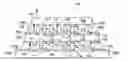
FIG. 1 is a schematic diagram of an exemplary integrated circuit underfill structure according to some embodiments; and
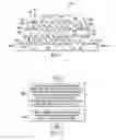
FIG. 2 is a flowchart of a method of fabricating the exemplary integrated circuit underfill structure in FIG. 1 according to some embodiments.
DETAILED DESCRIPTION
The making and using of various embodiments are discussed in detail below. It should be appreciated, however, that the present disclosure provides many applicable inventive concepts that can be embodied in a wide variety of specific contexts. The specific embodiments discussed are merely illustrative of specific ways to make and use, and do not limit the scope of the disclosure.
In addition, the present disclosure may repeat reference numerals and/or letters in the various examples. This repetition is for the purpose of simplicity and clarity and does not in itself dictate a relationship between the various embodiments and/or configurations discussed. Moreover, the formation of a feature on, connected to, and/or coupled to another feature in the present disclosure that follows may include embodiments in which the features are formed in direct contact, and may also include embodiments in which additional features may be formed interposing the features, such that the features may not be in direct contact. In addition, spatially relative terms, for example, “lower,” “upper,” “horizontal,” “vertical,” “above,” “over,” “below,” “beneath,” “up,” “down,” “top,” “bottom,” etc. as well as derivatives thereof (e.g., “horizontally,” “downwardly,” “upwardly,” etc.) are used for ease of the present disclosure of one features relationship to another feature. The spatially relative terms are intended to cover different orientations of the device including the features.
FIG. 1 is a schematic diagram of an exemplary integrated circuit underfill structure according to some embodiments. An integrated circuit 100 includes a substrate 102 and (integrated circuit) chips 104 and 106. The substrate 102 can be a silicon substrate (or any other suitable material), another integrated circuit chip, or a printed circuit board (PCB). The substrate 102 and/or chips 104 and 106 may include electrical devices or components fabricated on the surface, e.g., transistors, resistors, capacitors, etc. in some embodiments. The chip 104 can be an interposer in some embodiments.
The chip 104 is disposed over the substrate 102 and the chip 106 is disposed over the chip 104. Even though two chips 104 and 106 are shown over the substrate 102, there can be one chip, three or more chips over the substrate 102 stacked vertically. The substrate 102 and the chips 104 and 106 can be flip-chip bonded, 2.5D die-stacked, 3D die-stacked, or combined by any other methods. Solder bumps 112 and 114 are disposed between the substrate 102 and the chips 104 and 106, and provide interconnections. The solder bumps 112 and 114 can be micro solder bumps or ball grid array (BGA) solder bumps, for example, and have diameter/heights ranging from 10 μm to 800 μm in some embodiments.
Insulating films 108a and 108b are disposed around the solder bumps 112 and 114 respectively. The insulating films 108a and 108b provide electrical insulation for the solder bumps 112 and 114 except areas for interconnections such as 117. In some embodiments, the insulating films 108a and 108b cover some chip areas such as 118 between the solder bumps 112 or 114. In some embodiments, the substrate 102 and chips 104 and 106 may also have passivation or dielectric layers on the surfaces (not shown) for electrical insulation, such as silicon nitride or silicon dioxide.
The insulating films 108a and 108b are conformal to the solder bumps 112 and 114 (i.e. they maintain the general shape of the underlying topography, by having a uniform thickness), and have a thickness ranging from 500 angstrom to 20 μm in some embodiments. The insulating films 108a and 108b are formed (or coated) by atomic layer deposition or chemical vapor deposition, for example. The insulating films 108a and 108b comprise silicon dioxide, hafnium oxide, titanium oxide, zirconium oxide, polymer, aluminum oxide, other metal oxide, any combination thereof, or any other suitable material.
Thermally conductive underfill 110a and 110b, disposed between the substrate 102, the chips 104 and 106, and the solder bumps 112 and 114, provide protection and mechanical strength for the integrated circuit 100. Also, the underfill 110a and 110b compensate for any thermal expansion difference between the substrate 102 and chips 104 and 106. The underfill 110a and 110b are formed by dispensing and curing the underfill and the dispensing is performed by needle dispensing or jet dispensing in some embodiments.
The underfill 110a and 110b have a thermal conductivity of at least 0.5 W/mK in some embodiments for good heat conductivity. Heat dissipation is indicated by arrows 116, for example. In some embodiments, the underfill 110a and 110b comprise polymer such as commercially available Epo-TEK T7109 epoxy, which has a thermal conductivity of about 1.5 W/mK and an electrical resistivity of about 1013 ohm-cm. This provides a better thermal conductivity compared to some other material such as commercially available LOCTITE epoxy, which has a thermal conductivity of about 0.2 W/mK and an electrical resistivity of about 1016 ohm-cm. As a result, the integrated circuit 100 has improved thermal conductivity between the substrate 102 and stacked chips 104 and 106.
FIG. 2 is a flowchart of a method of fabricating the exemplary integrated circuit underfill structure in FIG. 1 according to some embodiments. At step 202, an insulating film is formed around solder bumps disposed between a substrate and at least one chip. The insulating film provides electrical insulation for the solder bumps except areas for interconnections. Each chip is disposed over the substrate or the other chip. The insulating film is formed (or coated) by atomic layer deposition or chemical vapor deposition, for example.
The insulating film is conformal to the solder bumps and has a thickness ranging from 500 angstrom to 20 μm in some embodiments. The insulating film comprises silicon dioxide, hafnium oxide, titanium oxide, zirconium oxide, polymer, aluminum oxide, other metal oxide, any combination thereof, or any other suitable material. The insulating film is formed to cover chip areas between the solder bumps in some embodiments.
At step 204, a thermally conductive underfill is formed between the substrate, the at least one chip, and the solder bumps. The thermally conductive underfill has a thermal conductivity of at least 0.5 W/mK in some embodiments for better heat conductivity. The thermally conductive underfill comprises polymer. In some embodiments, the underfill comprises commercially available Epo-TEK T7109 epoxy, which has a thermal conductivity of about 1.5 W/mK and an electrical resistivity of about 1013 ohm-cm. The underfill is formed by dispensing and curing the underfill, and the dispensing is performed by needle dispensing or jet dispensing in some embodiments.
According to some embodiments, an integrated circuit includes a substrate and at least one chip. Each chip is disposed over the substrate or the other chip. Solder bumps are disposed between the substrate and the at least one chip. An insulating film is disposed around the solder bumps and provides electrical insulation for the solder bumps except areas for interconnections. A thermally conductive underfill is disposed between the substrate, the at least one chip, and the solder bumps.
According to some embodiments, a method includes forming an insulating film around solder bumps disposed between a substrate and at least one chip. Each chip is disposed over the substrate or the other chip. The insulating film provides electrical insulation for the solder bumps except areas for interconnections. A thermally conductive underfill is formed between the substrate, the at least one chip, and the solder bumps.
According to some embodiments, an integrated circuit includes a substrate and at least one chip. Each chip is disposed over the substrate or the other chip. Solder bumps are disposed between the substrate and the at least one chip and provide interconnections. An insulating film is disposed around the solder bumps. The insulating film provides electrical insulation for the solder bumps except the interconnections provided by the solder bumps. A thermally conductive underfill is disposed between the substrate, the at least one chip, and the solder bumps. The thermally conductive underfill comprises polymer having a thermal conductivity of at least 0.5 W/mK.
A skilled person in the art will appreciate that there can be many embodiment variations of this disclosure. Although the embodiments and their features have been described in detail, it should be understood that various changes, substitutions and alterations can be made herein without departing from the spirit and scope of the embodiments. Moreover, the scope of the present application is not intended to be limited to the particular embodiments of the process, machine, manufacture, and composition of matter, means, methods and steps described in the specification. As one of ordinary skill in the art will readily appreciate from the disclosed embodiments, processes, machines, manufacture, compositions of matter, means, methods, or steps, presently existing or later to be developed, that perform substantially the same function or achieve substantially the same result as the corresponding embodiments described herein may be utilized according to the present disclosure.
The above method embodiment shows exemplary steps, but they are not necessarily required to be performed in the order shown. Steps may be added, replaced, changed order, and/or eliminated as appropriate, in accordance with the spirit and scope of embodiment of the disclosure. Embodiments that combine different claims and/or different embodiments are within the scope of the disclosure and will be apparent to those skilled in the art after reviewing this disclosure.
Claims
What is claimed is:1. A method comprising:
coating an insulating film on solder bumps disposed between a substrate and a chip; and
forming a thermally conductive underfill between the substrate, the chip, and the solder bumps, the thermally conductive underfill surrounding the solder bumps and the insulating film on the solder bumps.
2. The method of claim 1, wherein the forming the thermally conductive underfill further comprises:
dispensing the thermally conductive underfill between the substrate, the chip, and the solder bumps; and
curing the dispensed thermally conductive underfill.
3. The method of claim 2, wherein the dispensing the thermally conductive underfill is performed by needle dispensing or jet dispensing the thermally conductive underfill.
4. The method of claim 1, wherein the insulating film has a substantially uniform thickness on sidewalls of the solder bumps as measured from the sidewalls of the solder bumps in a direction substantially perpendicular to the sidewalls of the solder bumps.
5. The method of claim 1, wherein the thermally conductive underfill has a thermal conductivity of at least 0.5 W/mK.
6. The method of claim 1, wherein the thermally conductive underfill comprises a polymer.
7. The method of claim 1, wherein the insulating film comprises aluminum oxide, hafnium oxide, silicon dioxide, titanium oxide, zirconium oxide, polymer, or any combination thereof.
8. The method of claim 1, wherein the coating the insulating film on solder bumps further comprises forming the insulating film on solder bumps by a chemical vapor deposition process.
9. The method of claim 1, wherein the coating the insulating film on solder bumps further comprises forming the insulating film on solder bumps by an atomic layer deposition process.
10. A method comprising:
bonding a first side of a first chip to a substrate with a first set of conductive connectors;
forming a first insulating film on the first set of conductive connectors; and
forming a first thermally conductive underfill between the substrate, the first side of the first chip, and the first set of conductive connectors, the first thermally conductive underfill surrounding the first set of conductive connectors and the first insulating film on the first set of conductive connectors.
11. The method of claim 10, wherein the first set of conductive connectors comprise a solder material.
12. The method of claim 10, wherein the first insulating film has a substantially uniform thickness on sidewalls of the first set of conductive connectors as measured from the sidewalls of the first set of conductive connectors in a direction substantially perpendicular to the sidewalls of the first set of conductive connectors.
13. The method of claim 10 further comprising:
bonding a second chip to a second side of the first chip with a second set of conductive connectors, the second side being opposite the first side;
forming a second insulating film on the first set of conductive connectors; and
forming a second thermally conductive underfill between the second side of the first chip, the second chip, and the second set of conductive connectors, the second thermally conductive underfill surrounding the second set of conductive connectors and the second insulating film on the second set of conductive connectors.
14. The method of claim 10, wherein the first thermally conductive underfill has a thermal conductivity of at least 0.5 W/mK.
15. The method of claim 10, wherein the first thermally conductive underfill comprises a polymer.
16. The method of claim 10, wherein the forming a first insulating film on the first set of conductive connectors further comprises forming the first insulating film on the first set of conductive connectors by a chemical vapor deposition process.
17. A device comprising:
a first set of solder bumps bonding a substrate to a first chip;
a first insulating film contacting the first set of solder bumps, a first surface of the first chip, and a surface of the substrate; and
a first thermally conductive underfill between the substrate, the first chip, and the first set of solder bumps.
18. The device of claim 17, wherein the first thermally conductive underfill has a thermal conductivity of at least 0.5 W/mK.
19. The device of claim 17, wherein the first insulating film has a substantially uniform thickness on sidewalls of the first set of solder bumps as measured from the sidewalls of the first set of solder bumps in a direction substantially perpendicular to the sidewalls of the first set of solder bumps.
20. The device of claim 17 further comprising:
a second set of solder bumps bonding a second chip to the first chip, the first chip being between the second chip and the substrate;
a second insulating film contacting the second set of solder bumps, a second surface of the first chip, and a surface of the second chip; and
a second thermally conductive underfill between the substrate, the second chip, and the second set of solder bumps.
Images & Drawings included:
Sources:
- United States Patent and Trademark Office - verify current appl. status at the USPTO↗
Similar patent applications:
Recent applications in this class:
- » 20250273622 2025-08-28
ELECTRONIC PACKAGE AND MANUFACTURING METHOD THEREOF - » 20250266391 2025-08-21
LASER ASSISTED BONDING METHOD - » 20250259964 2025-08-14
MOLDED SPACER FOR SURFACE MOUNT TECHNOLOGY - » 20250246576 2025-07-31
ELECTRONIC DEVICE AND A METHOD FOR FORMING THE SAME - » 20250226358 2025-07-10
PRE-ATTACHED ENGINEERED SOLDERS FOR ULTRA-LOW RESIDUE SOLDERING - » 20250226357 2025-07-10
ELECTRICAL CIRCUIT FORMATION METHOD AND ELECTRICAL CIRCUIT FORMATION DEVICE - » 20250219019 2025-07-03
SEMICONDUCTOR DEVICE AND METHOD FOR MANUFACTURING THE SAME - » 20250219018 2025-07-03
SEMICONDUCTOR PACKAGING METHOD, SEMICONDUCTOR ASSEMBLY COMPONENT AND ELECTRONIC DEVICE - » 20250219017 2025-07-03
DIE-BONDING METHOD FOR PREVENTING DIE FROM BENDING - » 20250210584 2025-06-26
METHOD OF BONDING LIGHT EMITTING ELEMENT AND METHOD OF MANUFACTURING DISPLAY DEVICE, HAVING THE SAME
Recent applications for this Assignee:
- » 20240266341 2024-08-08
HYBRID BONDING WITH UNIFORM PATTERN DENSITY - » 20240224489 2024-07-04
SEMICONDUCTOR DEVICE - » 20240170063 2024-05-23
CONTENT ADDRESSABLE MEMORY ARRAY DEVICE STRUCTURE - » 20240161819 2024-05-16
MEMORY DEVICE AND MANUFACTURING THEREOF - » 20240153896 2024-05-09
SEMICONDUCTOR PACKAGE SYSTEM AND METHOD - » 20240120409 2024-04-11
Method for non-resist nanolithography - » 20240113080 2024-04-04
Semiconductor Device with Discrete Blocks - » 20240105632 2024-03-28
Method for forming a semiconductor device including forming a first interconnect structure on one side of a substrate having first metal feature closer the substrate than second metal feature and forming first and second tsv on other side of substrate connecting to the metal features - » 20240096816 2024-03-21
Method of manufacture overlay mark using laser marking process for semiconductor device - » 20240096383 2024-03-21
MEMORY DEVICE