Cavity package with pre-molded cavity leadframe
US20160126164A1
2016-05-05
14/993,175
2016-01-12
✅ Patent granted
US 9,536,812 B2
2017-01-03
-
-
Nathan W Ha
Keating and Bennett, LLP
2036-01-12
Abstract:
A cavity package is disclosed comprising a metal leadframe, a metal ring connected to the metal leadframe, a plastic body molded to the metal leadframe forming a substrate cavity including an exposed die attach pad of the leadframe for affixing a semiconductor device, exposed lead fingers of the leadframe for wire bonding to the semiconductor device and an external circuit, and an exposed top surface of the metal ring, and a metal cap for closing and encapsulating the substrate cavity. The metal ring is integrated into the pre-molded cavity leadframe for providing an electrical ground path from the metal cap to the die attach pad and permitting attachment of the metal cap to the pre-molded leadframe using solder reflow.
Assignee:
- UBOTIC COMPANY LIMITED 4 🇨🇳 Hong Kong, China
Applicant:
Interested in similar patents?
Get notified when new applications in this technology area are published.
Classification:
H01L21/4825 » CPC further
Processes or apparatus adapted for the manufacture or treatment of semiconductor or solid state devices or of parts thereof; Manufacture or treatment of semiconductor devices or of parts thereof the devices having at least one potential-jump barrier or surface barrier, e.g. PN junction, depletion layer or carrier concentration layer; Manufacture or treatment of parts, e.g. containers, prior to assembly of the devices, using processes not provided for in a single one of the subgroups -; Conductive parts; Flat leads, e.g. lead frames with or without insulating supports Connection or disconnection of other leads to or from flat leads, e.g. wires, bumps, other flat leads
H01L21/565 » CPC further
Processes or apparatus adapted for the manufacture or treatment of semiconductor or solid state devices or of parts thereof; Manufacture or treatment of semiconductor devices or of parts thereof the devices having at least one potential-jump barrier or surface barrier, e.g. PN junction, depletion layer or carrier concentration layer; Assembly of semiconductor devices using processes or apparatus not provided for in a single one of the subgroups - , e.g. sealing of a cap to a base of a container; Encapsulations, e.g. encapsulation layers, coatings Moulds
H01L23/3114 » CPC further
Details of semiconductor or other solid state devices; Encapsulations, e.g. encapsulating layers, coatings, e.g. for protection characterised by the arrangement or shape the device being completely enclosed the device being a chip scale package, e.g. CSP
H01L23/4952 » CPC further
Details of semiconductor or other solid state devices; Arrangements for conducting electric current to or from the solid state body in operation, e.g. leads, terminal arrangements ; Selection of materials therefor consisting of soldered constructions; Lead-frames or other flat leads; Additional leads the additional leads being a bump or a wire
H01L23/49541 » CPC further
Details of semiconductor or other solid state devices; Arrangements for conducting electric current to or from the solid state body in operation, e.g. leads, terminal arrangements ; Selection of materials therefor consisting of soldered constructions; Lead-frames or other flat leads Geometry of the lead-frame
H01L23/49582 » CPC further
Details of semiconductor or other solid state devices; Arrangements for conducting electric current to or from the solid state body in operation, e.g. leads, terminal arrangements ; Selection of materials therefor consisting of soldered constructions; Lead-frames or other flat leads characterised by the materials of the lead frames or layers thereon Metallic layers on lead frames
H01L23/495 IPC
Details of semiconductor or other solid state devices; Arrangements for conducting electric current to or from the solid state body in operation, e.g. leads, terminal arrangements ; Selection of materials therefor consisting of soldered constructions Lead-frames or other flat leads
H01L21/48 IPC
Processes or apparatus adapted for the manufacture or treatment of semiconductor or solid state devices or of parts thereof; Manufacture or treatment of semiconductor devices or of parts thereof the devices having at least one potential-jump barrier or surface barrier, e.g. PN junction, depletion layer or carrier concentration layer Manufacture or treatment of parts, e.g. containers, prior to assembly of the devices, using processes not provided for in a single one of the subgroups -
H01L21/56 IPC
Processes or apparatus adapted for the manufacture or treatment of semiconductor or solid state devices or of parts thereof; Manufacture or treatment of semiconductor devices or of parts thereof the devices having at least one potential-jump barrier or surface barrier, e.g. PN junction, depletion layer or carrier concentration layer; Assembly of semiconductor devices using processes or apparatus not provided for in a single one of the subgroups - , e.g. sealing of a cap to a base of a container Encapsulations, e.g. encapsulation layers, coatings
H01L21/78 » CPC further
Processes or apparatus adapted for the manufacture or treatment of semiconductor or solid state devices or of parts thereof; Manufacture or treatment of devices consisting of a plurality of solid state components formed in or on a common substrate or of parts thereof; Manufacture of integrated circuit devices or of parts thereof; Manufacture or treatment of devices consisting of a plurality of solid state components or integrated circuits formed in, or on, a common substrate with subsequent division of the substrate into plural individual devices
H01L21/50 » CPC further
Processes or apparatus adapted for the manufacture or treatment of semiconductor or solid state devices or of parts thereof; Manufacture or treatment of semiconductor devices or of parts thereof the devices having at least one potential-jump barrier or surface barrier, e.g. PN junction, depletion layer or carrier concentration layer Assembly of semiconductor devices using processes or apparatus not provided for in a single one of the subgroups - , e.g. sealing of a cap to a base of a container
H01L23/49575 » CPC further
Details of semiconductor or other solid state devices; Arrangements for conducting electric current to or from the solid state body in operation, e.g. leads, terminal arrangements ; Selection of materials therefor consisting of soldered constructions; Lead-frames or other flat leads Assemblies of semiconductor devices on lead frames
H01L23/10 » CPC further
Details of semiconductor or other solid state devices; Containers; Seals characterised by the material or arrangement of seals between parts, e.g. between cap and base of the container or between leads and walls of the container
H01L23/49861 » CPC further
Details of semiconductor or other solid state devices; Arrangements for conducting electric current to or from the solid state body in operation, e.g. leads, terminal arrangements ; Selection of materials therefor consisting of soldered constructions; Leads, on insulating substrates, Lead-frames fixed on or encapsulated in insulating substrates
H01L24/97 » CPC further
Arrangements for connecting or disconnecting semiconductor or solid-state bodies; Methods or apparatus related thereto; Batch processes at chip-level, i.e. with connecting carried out on a plurality of singulated devices, i.e. on diced chips the devices being connected to a common substrate, e.g. interposer, said common substrate being separable into individual assemblies after connecting
H01L23/49537 » CPC further
Details of semiconductor or other solid state devices; Arrangements for conducting electric current to or from the solid state body in operation, e.g. leads, terminal arrangements ; Selection of materials therefor consisting of soldered constructions; Lead-frames or other flat leads Plurality of lead frames mounted in one device
H01L24/32 » CPC further
Arrangements for connecting or disconnecting semiconductor or solid-state bodies; Methods or apparatus related thereto; Means for bonding being attached to, or being formed on, the surface to be connected, e.g. chip-to-package, die-attach, "first-level" interconnects; Manufacturing methods related thereto; Layer connectors, e.g. plate connectors, solder or adhesive layers; Manufacturing methods related thereto; Structure, shape, material or disposition of the layer connectors after the connecting process of an individual layer connector
H01L24/73 » CPC further
Arrangements for connecting or disconnecting semiconductor or solid-state bodies; Methods or apparatus related thereto Means for bonding being of different types provided for in two or more of groups , , , , , , ,
H01L24/85 » CPC further
Arrangements for connecting or disconnecting semiconductor or solid-state bodies; Methods or apparatus related thereto; Methods for connecting semiconductor or other solid state bodies using means for bonding being attached to, or being formed on, the surface to be connected using a wire connector
H01L24/92 » CPC further
Arrangements for connecting or disconnecting semiconductor or solid-state bodies; Methods or apparatus related thereto; Methods for connecting semiconductor or solid state bodies including different methods provided for in two or more of groups - Specific sequence of method steps
H01L2224/73265 » CPC further
Indexing scheme for arrangements for connecting or disconnecting semiconductor or solid-state bodies and methods related thereto as covered by; Means for bonding being of different types provided for in two or more of groups; Location after the connecting process on different surfaces Layer and wire connectors
H01L2224/92247 » CPC further
Indexing scheme for arrangements for connecting or disconnecting semiconductor or solid-state bodies and methods related thereto as covered by; Methods for connecting semiconductor or solid state bodies including different methods provided for in two or more of groups - ; Specific sequence of method steps; Connecting different surfaces of the semiconductor or solid-state body with connectors of different types; Sequential connecting processes the first connecting process involving a layer connector the second connecting process involving a wire connector
H01L2224/97 » CPC further
Indexing scheme for arrangements for connecting or disconnecting semiconductor or solid-state bodies and methods related thereto as covered by; Batch processes at chip-level, i.e. with connecting carried out on a plurality of singulated devices, i.e. on diced chips the devices being connected to a common substrate, e.g. interposer, said common substrate being separable into individual assemblies after connecting
H01L2924/15747 » CPC further
Indexing scheme for arrangements or methods for connecting or disconnecting semiconductor or solid-state bodies as covered by; Details of package parts other than the semiconductor or other solid state devices to be connected; Die mounting substrate; Material with a principal constituent of the material being a metal or a metalloid, e.g. boron [B], silicon [Si], germanium [Ge], arsenic [As], antimony [Sb], tellurium [Te] and polonium [Po], and alloys thereof the principal constituent melting at a temperature of greater than or equal to 950 C and less than 1550 C Copper [Cu] as principal constituent
H01L2924/165 » CPC further
Indexing scheme for arrangements or methods for connecting or disconnecting semiconductor or solid-state bodies as covered by; Details of package parts other than the semiconductor or other solid state devices to be connected; Cap; Connection portion, e.g. seal; Material with a principal constituent of the material being a metal or a metalloid, e.g. boron [B], silicon [Si], germanium [Ge], arsenic [As], antimony [Sb], tellurium [Te] and polonium [Po], and alloys thereof
H01L2924/167 » CPC further
Indexing scheme for arrangements or methods for connecting or disconnecting semiconductor or solid-state bodies as covered by; Details of package parts other than the semiconductor or other solid state devices to be connected; Cap; Material with a principal constituent of the material being a metal or a metalloid, e.g. boron [B], silicon [Si], germanium [Ge], arsenic [As], antimony [Sb], tellurium [Te] and polonium [Po], and alloys thereof
H01L2924/16251 » CPC further
Indexing scheme for arrangements or methods for connecting or disconnecting semiconductor or solid-state bodies as covered by; Details of package parts other than the semiconductor or other solid state devices to be connected; Cap; Disposition Connecting to an item not being a semiconductor or solid-state body, e.g. cap-to-substrate
H01L23/498 IPC
Details of semiconductor or other solid state devices; Arrangements for conducting electric current to or from the solid state body in operation, e.g. leads, terminal arrangements ; Selection of materials therefor consisting of soldered constructions Leads, on insulating substrates,
H01L23/00 IPC
Details of semiconductor or other solid state devices
H01L23/31 IPC
Details of semiconductor or other solid state devices; Encapsulations, e.g. encapsulating layers, coatings, e.g. for protection characterised by the arrangement or shape
H01L24/48 » CPC further
Arrangements for connecting or disconnecting semiconductor or solid-state bodies; Methods or apparatus related thereto; Means for bonding being attached to, or being formed on, the surface to be connected, e.g. chip-to-package, die-attach, "first-level" interconnects; Manufacturing methods related thereto; Wire connectors; Manufacturing methods related thereto; Structure, shape, material or disposition of the wire connectors after the connecting process of an individual wire connector
H01L2924/1659 » CPC further
Indexing scheme for arrangements or methods for connecting or disconnecting semiconductor or solid-state bodies as covered by; Details of package parts other than the semiconductor or other solid state devices to be connected; Cap; Connection portion, e.g. seal; Material with a principal constituent of the material being a polymer, e.g. polyester, phenolic based polymer, epoxy
H01L23/49503 » CPC main
Details of semiconductor or other solid state devices; Arrangements for conducting electric current to or from the solid state body in operation, e.g. leads, terminal arrangements ; Selection of materials therefor consisting of soldered constructions; Lead-frames or other flat leads characterised by the die pad
H01L23/047 » CPC further
Details of semiconductor or other solid state devices; Containers; Seals characterised by the shape of the container or parts, e.g. caps, walls the container being a hollow construction and having a conductive base as a mounting as well as a lead for the semiconductor body the other leads being parallel to the base
H01L2924/15153 » CPC further
Indexing scheme for arrangements or methods for connecting or disconnecting semiconductor or solid-state bodies as covered by; Details of package parts other than the semiconductor or other solid state devices to be connected; Die mounting substrate; Shape the die mounting substrate comprising a recess for hosting the device
Description
RELATED APPLICATIONS
This application claims priority from U.S. patent application 61/870,354, filed Aug. 27, 2013. Priority is claimed to this earlier filed application and the contents of this earlier-filed application are incorporated herein, in their entirety, by reference.
FIELD OF INVENTION
The present invention relates generally to integrated circuits, and more particularly to a cavity package with a pre-molded cavity leadframe.
BACKGROUND
Flat no-leads packages such as QFN (quad-flat no-leads) and DFN (dual-flat no-leads) are used to physically and electrically connect integrated circuits to printed circuit boards. Two types of flat no-leads packages are common: cavity (i.e. with a cavity designed into the package containing air or nitrogen), and plastic-molded (i.e. with minimal air in the package). The cavity package is usually made up of three parts; a copper leadframe, plastic-molded body (open, and not sealed), and a cap or lid attached to the plastic portion of the leadframe. An integrated circuit (IC) is mounted to a die attach pad within the cavity, with wire leads connecting the IC to the leadframe. The leadframe terminates in contacts on the bottom of the package for providing electrical interconnection with a printed circuit board.
Cavity packages are small and lightweight, with good thermal and electrical performance that makes them suitable for portable communication/consumer products. Applications include cellular phones, PDAs, wireless transmitters, RF front end, HD devices, microcontrollers, pre-amplifiers, servers, smart power suppliers, switches, DSPs, ASICs and wrist watches.
SUMMARY
According to an aspect of the invention, a metal ring is integrated into the pre-molded cavity leadframe. The metal ring provides an electrical ground path from the metal cap to the die attach pad and permits attachment of the metal cap to the pre-molded leadframe using solder reflow onto.
BRIEF DESCRIPTION OF THE DRAWINGS
Features and advantages of the invention will be apparent from the detailed description which follows, taken in conjunction with the accompanying drawings, which together illustrate, by way of example, features of the invention; and, wherein:
FIG. 1 is a flowchart showing steps in a process for constructing a cavity package with a pre-molded cavity leadframe, according to exemplary embodiments.
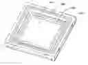
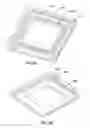
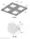
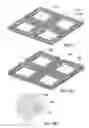
FIGS. 2A and 2B are top and bottom perspective views, respectively, of a cavity package with a pre-molded cavity leadframe, according to an exemplary embodiment.
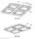
FIGS. 3A and 3B are top and bottom perspective views, respectively, of a cap for the cavity package of FIGS. 2A and 2B.
FIGS. 4A and 4B are top and bottom perspective views, respectively, of a pre-molded cavity leadframe for the cavity package of FIGS. 2A and 2B.
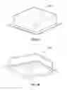
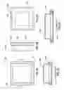
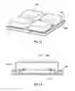
FIG. 5A is a top view of the cavity package with pre-molded cavity leadframe of FIGS. 2A and 2B.
FIG. 5B is a side view of the cavity package with pre-molded cavity leadframe of FIGS. 2A and 2B.
FIG. 5C is a bottom view of the cavity package with pre-molded cavity leadframe of FIGS. 2A and 2B.
FIG. 5D is a cross-sectional view of the cavity package with pre-molded cavity leadframe along the line A-A in FIG. 5A.
FIG. 5E is a cross-sectional view of the cavity package with pre-molded cavity leadframe along the line B-B in FIG. 5A.
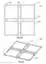
FIGS. 6A and 6B are top and perspective views, respectively, of a frame of seal rings fabricated in a matrix, according to one step of the process set forth in FIG. 1.
FIGS. 7A and 7B are a top perspective and a detail view, respectively, of the matrix of seal rings with supporting and connecting leads formed according to a further step of the process set forth in FIG. 1.
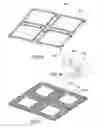
FIG. 8 is a perspective view of a matrix of bottom leadframes fabricated according to a further step of the process set forth in FIG. 1.
FIGS. 9A and 9B are a top perspective and a detail view, respectively, showing attachment of the frame of seal rings to the leadframe matrix via the supporting and connecting leads, according to a further step of the process set forth in FIG. 1.
FIGS. 10A and 10 B are top and bottom perspective views, respectively, of the leadframe matrix molded to create a cavity with exposed die attach pad, according to a further step of the process set forth in FIG. 1.
FIG. 11 is a top perspective view of the pre-molded leadframe matrix, after die attach on the respective die attach pads and wire bonding, according to a further step of the process set forth in FIG. 1, and after attachment of respective caps, according to another step of the process set forth in FIG. 1.
FIG. 12 is a cross-section view of a single cavity package, showing die attachment, wire bonding, and cap attachment, after singulation of the matrix according to a last step of the process set forth in FIG. 1.
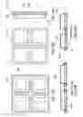
FIG. 13A is a bottom view of a pre-molded leadframe matrix according to an alternative embodiment, wherein solder balls are used to attach the frame of seal rings to the leadframe matrix.
FIG. 13B is a top view of the pre-molded leadframe matrix of FIG. 13A.
FIG. 13C is a side view of the pre-molded leadframe matrix of FIG. 13A.
FIG. 13D is a cross-sectional view of the pre-molded leadframe matrix along the line A-A in FIG. 13B.
FIG. 13E is a cross-sectional view of the pre-molded leadframe matrix along the line B-B in FIG. 13B.
FIG. 14 is a top perspective view of the pre-molded leadframe matrix, after placement of solder balls, according to a first sub-step of an alternative of one step of the process set forth in FIG. 1.
FIGS. 15A and 15B are a top perspective and a detail view, respectively, showing attachment of the frame of seal rings to the leadframe matrix via the solder balls, according to second sub-step of the alternative referred to with respect to FIG. 14.
Reference will now be made to the exemplary embodiments illustrated, and specific language will be used herein to describe the same. It will nevertheless be understood that no limitation of the scope of the invention is thereby intended.
DETAILED DESCRIPTION OF EXAMPLE EMBODIMENTS
Before the present invention is disclosed and described, it is to be understood that this invention is not limited to the particular structures, process steps, or materials disclosed herein, but is extended to equivalents thereof as would be recognized by those ordinarily skilled in the relevant arts. It should also be understood that terminology employed herein is used for the purpose of describing particular embodiments only and is not intended to be limiting.
With reference to FIGS. 1 through 13, construction of a cavity package 200 with a pre-molded cavity leadframe is shown, according to an exemplary embodiment.
As discussed above, and as shown in FIGS. 2A and 2B, the cavity package 200 comprises a copper leadframe 210, a plastic-molded body 220, and a lid or cap 230.
FIGS. 3A and 3B show the cap 230 used to enclose the attached semiconductor die within the pre-molded leadframe.
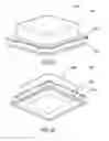
FIGS. 4A and 4B show the pre-molded leadframe comprising copper leadframe 210 molded within body 220, including a seal ring 400, exposed die attach pad 410, and exposed lead fingers 420 for wire bonding to the semiconductor device at the top surface and for soldering to an external circuit such as a PCB board, at the bottom surface thereof.
FIG. 5A is a top view of the cavity package with pre-molded cavity leadframe of FIGS. 2A and 2B, while FIG. 5B is a side view, FIG. 5C is a bottom view, FIG. 5D is a cross-sectional view along the line A-A in FIG. 5A, and FIG. 5E is a cross-sectional view along the line B-B in FIG. 5A.
Construction of the cavity package involves a two-part process beginning with pre-mold cavity leadframe fabrication, followed by assembly, as shown in FIG. 1.
The pre-mold cavity leadframe fabrication begins at step 100 (FIG. 1) with etching or stamping of a metal (e.g. Cu, alloy 42, Al, etc.) frame of rings 400 that are held together by half-etched temporary tie bars 500, as shown in FIGS. 6A-6B, Each ring 400 includes supporting and connecting leads 510. Optionally, the frame of rings 400 can be plated by a solderable metal (e.g. Ag, Sn/Au, etc.)
At step 110, the supporting and connecting leads 510 are shaped by mechanical bending, for example using a punch tool and anvil block, so that the matrix of rings ‘stands’ on leads 510 at an appropriate height above the leadframe 200, as discussed in greater detail below.
At step 120, the leadframe 210 is fabricated in a matrix, as shown in FIG. 8. Step 120 can be performed before, after or simultaneously with step 100 or step 110.
At step 130, the metal frame of rings 400 is mechanically and electrically connected to the leadframe 210 (e.g. by conductive epoxy, soldering, spot welding, etc.), as shown in FIGS. 9A and 9B. The leads 510 are used to support the rings and prevent the structure from collapsing as a result of clamping pressure by the mold tool during a subsequent molding step. The ring 400 is electrically connected to the tie bar 910 of the die attach pad 410 for later electrical connection to the metal cap 230.
At step 140, leadframe 210 is molded in plastic molded body 220 to form a cavity 1000 for receiving the semiconductor device die in a subsequent step. The top side of the metal ring 400, a portion of the top side of the bonding fingers 420, the top side of the die attach pad 410, the bottom side of the bonding fingers 420 and the bottom side of the die attach pad 410 are all exposed after molding, as shown in FIGS. 10A and 10B.
FIG. 11 is a top perspective view of the pre-molded leadframe matrix, after die attach on the respective die attach pads and wire bonding, according to the assembly process of steps 150-170, and before singulation according to step 180.
The assembly process begins at step 150, wherein the semiconductor die 1300 is attached to the die attach pad 410 of the pre-molded leadframe 200, followed by wire bonding 1310, as shown in FIG. 12.
At step 160, the metal cap 230 is fabricated. Step 160 can be performed before, after or simultaneously with step 150.
At step 170, the cap 230 is attached to the top of the pre-molded cavity leadframe. The cap can be attached using conductive epoxy and solder reflow onto the exposed top surface of the metal seal ring 400 embedded into the pre-molded cavity leadframe. The metal ring 400 provides an electrical ground path from the metal cap 230 to the die attach pad 410 and permits attachment of the metal cap to the pre-molded leadframe using solder reflow.
After the cap 230 has been attached, at step 180, the matrix is singulated (e.g. using saw singulation) to create individual units.
Steps 150, 170 and 180 comprise the assembly process of the overall process of FIG. 1, following the pre-mold cavity leadframe fabrication process of steps 100-140. The cap fabrication step 160 can also form part of the pre-mold cavity leadframe fabrication process.
Referring again to step 130 of FIG. 1, it will be noted that the frame of rings 400 can be attached to the leadframe using the supporting and connecting leads 510, as discussed above and as depicted in FIGS. 6A, 6B, 7A, 7B, 9A and 9B. According to an alternative embodiment, solder balls can be used at step 130 instead of the supporting and connecting leads 510, as shown in FIGS. 13A-13E. In this alternative embodiment, step 110 is omitted.
According to a first sub-step of the alternative step 130, the solder ball contact area, the lead tips of each wire bond finger 420, and the periphery of the top surface of the die attach pad 410 on the leadframe 210 are selectively pre-plated by wire bondable and “solderable” metal (e.g. Ni/Au, Ni/Pd/Au, Ag, etc). The bottom exposed metal areas of the leadframe 210 are also selectively plated for surface mount reflow. The remainder of the non plated area of the leadframe 210 is then passivated (e.g. by oxidizing the base metal). Passivation acts as a solder resist for restricting undesired solder wetting. Solder balls 1500 are then placed as shown in FIG. 14.
FIGS. 15A and 15B are a top perspective and a detail view, respectively, showing attachment of the frame of seal rings 400 to the leadframe matrix 210 via the solder balls 1500, according to second sub-step of the alternative step 130. The solder ball contact area at the bottom surface of the ring 400 and the top exposed area of the ring are selectively pre-plated by “solderable” metal (e.g. Ni/Au, Ni/Pd/Au, Ag, . . . etc). The rest of the non plated area of the ring is then passivated (e.g. by oxidizing the base metal), wherein passivation acts as a solder resist to restrict undesired solder wetting. The rings 400 are then soldered onto the leadframe 210 by reflowing the solder balls 1500.
While the forgoing exemplary embodiment is illustrative of the principles of the present invention, it will be apparent to those of ordinary skill in the art that numerous modifications in form, usage and details of implementation can be made without the exercise of inventive faculty, and without departing from the principles and concepts of the invention. Accordingly, it is not intended that the invention be limited, except as by the claims set forth below.
Claims
What is claimed is:1. A method of manufacturing a cavity package comprising:
i) fabricating a frame of metal rings;
ii) fabricating a matrix of metal leadframes;
iii) attaching the frame of metal rings to the matrix of metal leadframes;
iv) molding the matrix of metal leadframes and attached rings to form a plurality of substrate cavities each including an exposed die attach pad for affixing a semiconductor device, exposed lead fingers for wire bonding to the semiconductor device and to an external circuit, and an exposed top surface of the frame of metal rings;
v) attaching a semiconductor device die to each die attach pad;
vi) wire bonding the semiconductor device to the lead fingers;
vii) fabricating a plurality of metal caps;
viii) attaching the plurality of metal caps to the rings via exposed top surfaces of the frame of metal rings for protecting the wire bonded semiconductor device die and electrically grounding the caps to the matrix of metal leadframes; and
ix) singulating the matrix into individual cavity packages.
2. The method of claim 1, further comprising forming supporting and connecting leads on the frame of metal rings.
3. The method of claim 2, wherein the frame of metal rings is attached to the matrix of metal leadframes via the supporting and connecting leads.
4. The method of claim 1, wherein the frame of metal rings is attached to the matrix of metal leadframes by reflowing solder balls placed on the matrix of metal leadframes and in contact with the rings.
Images & Drawings included:
Sources:
- United States Patent and Trademark Office - verify current appl. status at the USPTO↗
Similar patent applications:
Recent applications in this class:
- » 20250293123 2025-09-18
SEMICONDUCTOR DEVICE AND METHOD FOR MANUFACTURING THE SAME - » 20250285943 2025-09-11
LEADFRAME - » 20250266328 2025-08-21
PACKAGE STRUCTURE - » 20250259915 2025-08-14
SEMICONDUCTOR LEADFRAME PACKAGES AND RELATED METHODS - » 20250210470 2025-06-26
POLYMERIC DIE PAD FOR DIE ISOLATION IN CHIP ON LEAD PACKAGE - » 20250096077 2025-03-20
SEMICONDUCTOR DEVICE WITH ENHANCED SOLDERABILITY AND METHOD THEREFOR - » 20250069993 2025-02-27
PACKAGE STRUCTURE WITH PHOTONIC DIE AND METHOD - » 20250029899 2025-01-23
ELECTRONIC PACKAGE STRUCTURE - » 20250029898 2025-01-23
SEMICONDUCTOR DEVICE - » 20250022776 2025-01-16
LEAD FRAME FOR A DIE
Recent applications for this Assignee:
- » 20190063971 2019-02-28
Mass flow sensor module and method of manufacture - » 20150061094 2015-03-05
Cavity package with pre-molded cavity leadframe - » 20140306333 2014-10-16
Cavity package with die attach pad