P-type semiconductor composed of magnesium, silicon, tin, and germanium, and method for manufacturing the same
US20160149110A1
2016-05-26
14/900,439
2014-07-10
✅ Patent granted
US 9,666,782 B2
2017-05-30
WO; PCT/JP2014/068401; 20140710
WO; WO2015/012113; 20150129
Kyoung Lee
Oliff PLC
2034-07-10
Abstract:
A manufacturing method for a p-type semiconductor formed by sintering a compound represented by the general chemical formula: Mg2SiXSnYGeZ (where X+Y+Z=1, X>0, and Y>0, Z>0). The p-type semiconductor has a composition in which X is in the range of 0.00<X≦0.25, and Z satisfies the relationship: −1.00X+0.40≧Z≧−2.00X+0.10, where Z>0.00, and Y is in the range of 0.60≦Y≦0.95, and Z satisfies either of the relationships: −1.00Y+1.00≧Z≧−1.00Y+0.75, where 0.60≦Y≦0.90 and Z>0.00, and −2.00Y+1.90≧Z≧−1.00Y+0.75, where 0.90≦Y≦0.95 and Z>0.00.
Inventors:
- Yukihiro Isoda 5 🇯🇵 Tsukuba-shi, Japan
- Satoki TADA 4 🇯🇵 Kiryu-shi, Japan
- Hirofumi FUJIU 1 🇯🇵 Kiryu-shi, Japan
- Yukihiro Isoda 4 🇯🇵 Tsukuba, Japan
- Satoki Tada 3 🇯🇵 Kiryu, Japan
- Hirofumi Fujiu 1 🇯🇵 Kiryu, Japan
Assignee:
- National Institute For Materials Science 164 🇯🇵 Tsukuba-shi, Japan
- NATIONAL INSTITUTE FOR MATERIALS SCIENCE 166 🇯🇵 Tsukuba-shi, Ibaraki, Japan
- MITSUBA CORPORATION 100 🇯🇵 Kiryu-shi, Japan
- MITSUBA CORPORATION 100 🇯🇵 Kiryu-shi, Gunma, Japan
Applicant:
Interested in similar patents?
Get notified when new applications in this technology area are published.
Classification:
H01L35/14 » CPC further
Thermoelectric devices comprising a junction of dissimilar materials, i.e. exhibiting Seebeck or Peltier effect with or without other thermoelectric effects or thermomagnetic effects; Processes or apparatus peculiar to the manufacture or treatment thereof or of parts thereof; Details thereof; Selection of the material for the legs of the junction using inorganic compositions
C22C13/00 » CPC further
Alloys based on tin
H01L35/34 » CPC main
Thermoelectric devices comprising a junction of dissimilar materials, i.e. exhibiting Seebeck or Peltier effect with or without other thermoelectric effects or thermomagnetic effects; Processes or apparatus peculiar to the manufacture or treatment thereof or of parts thereof; Details thereof Processes or apparatus specially adapted for peculiar to the manufacture or treatment of these devices or of parts thereof
C22C23/00 » CPC further
Alloys based on magnesium
B22F2301/40 » CPC further
Metallic composition of the powder or its coating Intermetallics other than rare earth-Co or -Ni or -Fe intermetallic alloys
C22C1/04 » CPC further
Making alloys by powder metallurgy
C01B33/06 » CPC further
Silicon; Compounds thereof Metal silicides
C22C1/0408 » CPC further
Making alloys by powder metallurgy Light metal alloys
B22F3/14 » CPC further
Manufacture of workpieces or articles from metallic powder characterised by the manner of compacting or sintering; Apparatus specially adapted therefor ; Presses and furnaces; Both compacting and sintering simultaneously
Description
BACKGROUND
The present disclosure relates to a p-type semiconductor composed of magnesium, silicon, tin, and germanium, and a method for manufacturing the same.
Recently, attempts have been made to improve thermoelectric performance by reducing the resistivity by carrier concentration control by doping a Mg2Si-based material with a p-type dopant (for example, Ag, Ga, or Li). Examples of such materials include:
Mg2Si+1 at % Ag, ZT=0.1 (560 K): (See M. Akasaka et al., J. Appl. Phys., 104, 013703, 2008).
Mg2Si0.6Ge0.4+0.8% Ga, ZT=0.36 (625 K): (see H. Lhou-Mouko et al., J. Alloys Compd., 509, pp. 6503-6508, 2011).
Mg2Si0.25Sn0.75+Ag-20000 ppm and Li-5000 ppm, ZT=0.32 (600 K): (see Japanese Published Unexamined Patent Application No. 2010-37641).
SUMMARY
Mg2(SiSn) and Mg2(SiGe) have been studied as promising p-type semiconductors, however, there are no known attempts that have been developed into semiconductors on a practical level. P-type semiconductors Mg2(SiSn) and Mg2(SiGe) are solid solutions with Mg2Si, and it is believed that Ge and Sn contribute to p-type conduction in the solid solutions. Therefore, elements that can change the Si site of the base composition must form an anti-fluorite structure with Mg. Such metal elements are limited to silicon (Si), germanium (Ge), tin (Sn), and lead (Pb) of Group 14. However, Pb is generally excluded from this list of elements because it is a hazardous metal.
An attempt was made to improve the performance of a p-type thermoelectric semiconductor by using the following quaternary system:
Mg2SiXSnYGeZ, where X+Y+Z=1 and X>0, Y>0, Z>0.
When using ternary Mg2SiSn, only two phase diagrams of Mg2Si and Mg2Sn are considered. However, when using the above-mentioned quaternary system, four phase diagrams of Mg2Ge, Mg2(SiSn), Mg2(SiGe), and Mg2(SnGe) must be considered. As a result, preparation of a single-phase sample of the quaternary system is difficult. These are problems that the present disclosure is intended to solve.
In view of the circumstances described above, the present disclosure addresses the above-described problems. One embodiment according to the present disclosure provides a method for manufacturing a p-type semiconductor composed of magnesium, silicon, tin, and germanium. The method of manufacturing the p-type semiconductor involves sintering a compound represented by the following general chemical formula:
Mg2SiXSnYGeZ, where X+Y+Z=1 and X>0, Y>0, Z>0 and is obtained through liquid-solid reaction of magnesium, silicon, tin, and germanium as raw materials. The obtained semiconductor is a p-type semiconductor satisfying the following equations:
X is in the range of 0.00<X≦0.25, and Z satisfies the relationship of −1.00X+0.40≧Z≧−2.00X+0.10, where Z>0.00, and
Y is in the range of 0.60≦Y≦0.95, and Z satisfies either of the following relationships:
−1.00Y+1.00≧Z≧−1.00Y+0.75, when 0.60≦Y≦0.90 and Z>0.00, and
−2.00Y+1.90≧Z≧−1.00Y+0.75, when 0.90≦Y≦0.95 and Z>0.00.
Another embodiment according to the present disclosure provides a p-type semiconductor composed of magnesium, silicon, tin, and germanium. The p-type semiconductor is manufactured by sintering a material represented by the following general chemical formula:
Mg2SiXSnYGeZ, where X+Y+Z=1 and X>0, Y>0, Z>0 obtained through liquid-solid reaction of magnesium, silicon, tin, and germanium as raw materials.
The obtained semiconductor is a p-type semiconductor satisfying the following equations:
X is in the range of 0.00<X≦0.25, and Z satisfies the relationship:
−1.00X+0.40≧Z≧−2.00X+0.10, where Z>0.00, and
Y is in the range of 0.60≦Y≦0.95, and Z satisfies either of the following relationships:
−1.00Y+1.00≧Z≧−1.00Y+0.75, when 0.60≦Y≦0.90 and Z>0.00, and
−2.00Y+1.90≧Z≧−1.00Y+0.75, when 0.90≦Y≦0.95 and Z>0.00.
The above embodiments make it possible to easily manufacture a p-type semiconductor represented by the following general chemical formula:
Mg2SiXSnYGeZ, where X+Y+Z=1 and X>0, Y>0, Z>0.
BRIEF DESCRIPTION OF THE DRAWINGS
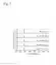
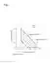
FIG. 1 is a process chart for obtaining a p-type semiconductor according to an embodiment of the present disclosure.
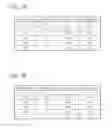
FIG. 2A is a table showing compositions of weighed values of p-type semiconductors, and FIG. 2B is a table showing compositions of p-type semiconductors according to the present disclosure.
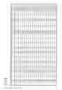
FIG. 3 is a graph showing X-ray diffraction measurement results of Mg2Si0.25SnYGeZ in various p-type semiconductors.
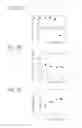
FIG. 4 is a table showing the compositions (weighed values) of Mg2SiXSnYGeZ and thermoelectric properties thereof at a room temperature in various p-type semiconductors.
FIG. 5A, FIG. 5B, and FIG. 5C are graphs showing the relationships between the Ge composition and the Seebeck coefficient α, the thermal conductivity κ, and the resistivity ρ in various p-type semiconductors.
FIG. 6 is a graph showing the relationship between X and Z in various p-type semiconductors.
FIG. 7 is a graph showing the relationship between Y and Z in various p-type semiconductors.
DETAILED DESCRIPTION OF THE EMBODIMENTS
The present disclosure provides a p-type semiconductor made of a sintered compact of an intermetallic compound of magnesium (Mg), silicon (Si), tin (Sn), and germanium (Ge), which is represented by the following general chemical formula:
Mg2SiXSnYGeZ, wherein X+Y+Z=1 and X>0, Y>0, Z>0. The sintered compact of the intermetallic compound is manufactured as follows.
Granular Mg and Sn with a grain size of approximately 2 to 10 mm are prepared, and powdery Si and Ge with a grain size of approximately several tens of μm are prepared. Predetermined amounts of these materials are weighed and put into a carbon board. The carbon board is covered with a carbon lid, and heated for 4 hours at an absolute temperature of 1173 K under an atmosphere of 0.1 MPa ArH2 (3 weight % hydrogen) to cause a liquid-solid reaction.
The obtained solid solution is pulverized into powder with a grain size of 38 to 75 μm, and sintered by hot-pressing. The sintering pressure is standardized to 50 MPa and the sintering time is standardized to 1 hour. The sintering temperature was determined according to each Sn composition amount Y. The sintering temperature is set to 1190 K when Y=0, 1040 K when Y=0.60 or 0.65, and 930 K when Y=0.75 or 0.90.
Weighed values (mole ratios) and compositions (mole ratios) of several sintered compacts obtained as described above are shown in the tables of FIG. 2. According to this, the weighed values (FIG. 2A) and the compositions (FIG. 2B) of the sintered compacts are found to have changed little when comparing the amounts of the Mg, Si, Sn and Ge before and after sintering.
Further, in FIG. 3, results of X-ray diffraction measurement of Mg2Si0.25SnYGeZ obtained as described above are shown. According to X-ray diffraction, peaks were observed with all of the sintered compacts existing between Mg2Si and Mg2Sn having an anti-fluorite structure. Only peaks caused by the anti-fluorite structure were observed, and no peaks were observed with oxides, Mg2Si, Mg2Ge, and Mg2Sn. Based on the data in FIG. 3, it was confirmed that all of the sintered compacts were single-phase. The same results were obtained with other sintered compacts.
Next, the conduction types, the Seebeck coefficients α (μV/K), the thermal conductivities κ (W/mK), and the resistivities ρ (Ωm) of various sintered compacts of Mg2SiXSnYGeZ thus obtained are shown in the table of FIG. 4. In FIG. 5, graphs showing the relationships between the Ge composition and the Seebeck coefficient α, the thermal conductivity κ, and the resistivity ρ are shown.
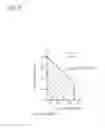
Next, conduction types of semiconductors with variable values for X and Z based on the results of FIG. 4 are plotted in FIG. 6. Conduction types of these semiconductors in which the values between Y and Z change are plotted in FIG. 7. From these graphs, the conduction type border between the p-type and the n-type is found to have changed linearly. In each graph, ∘ indicates p-type, and x indicates n-type.
First, observing the relationship between X and Z in FIG. 6, as a p-type semiconductor, X is in the range of 0.00<X≦0.25. When X is in this range, a maximum value Zmax and a minimum value Zmin of Z for obtaining a p-type semiconductor change linearly in relation to X. A linear function of Zmax and a linear function of Zmin are respectively obtained as follows:
Zmax=−1.00X+0.40
Zmin=−2.00X+0.10, where Zmin>0.00.
It is confirmed that, as a p-type semiconductor, X and Z fall within the shaded range shown in FIG. 6, that is, X and Z satisfy the following relationship:
−1.00X+0.40≧Z≧−2.00X+0.10, where Z>0.00.
Observing the relationship between Y and Z in FIG. 7, as a p-type semiconductor, Y is in the range of 0.60≦Y≦0.95. When Y is in this range, a maximum value Zmax and a minimum value Zmin of Z for obtaining a p-type semiconductor change linearly in relation to Y, and a linear function of Zmax and a linear function of Zmin are obtained as follows:
Zmax=−1.00Y+1.00, where 0.60≦Y≦0.90
Zmax=−2.00Y+1.90, where 0.90≦Y≦0.95
Zmin=−1.00Y+0.75, where Zmin>0.00.
It is confirmed that as a p-type semiconductor, Y and Z fall within the shaded range shown in FIG. 7, that is, Y and Z satisfy the following relationship:
−1.00Y+1.00≧Z≧−1.00Y+0.75, where 0.60≦Y≦0.90 and Z>0.00, or
−2.00Y+1.90≧Z≧−1.00Y+0.75, where 0.90≦Y≦0.95 and Z>0.00.
The present disclosure is applicable to obtaining of a p-type semiconductor composed of Mg2SiXSnYGeZ.
Claims
1. A method for manufacturing a p-type semiconductor composed of magnesium, silicon, tin, and germanium, comprising:
mixing magnesium, silicon, tin, and germanium as raw materials,
obtaining, by liquid-solid reaction, a solid solution of the magnesium, silicon, tin, and germanium mixture represented by the following general chemical formula:
Mg2SiXSnYGeZ, where X+Y+Z=1 and X>0, Y>0, Z>0, and
sintering the obtained mixture to produce a p-type semiconductor, the p-type semiconductor represented by the following general chemical formula:
Mg2SiXSnYGeZ, wherein:
X is in the range of 0.00<X≦0.25, and Z satisfies the relationship of −1.00X+0.40≧Z≧−2.00X+0.10, and Z>0.00, and
Y is in the range of 0.60≦Y≦0.95, and Z satisfies either of the following relationships:
−1.00Y+1.00≧Z≧−1.00Y+0.75, where 0.60≦Y≦0.90 and Z>0.00, and
−2.00Y+1.90≧Z≧−1.00Y+0.75, where 0.90≦Y≦0.95 and Z>0.00.
2. A p-type semiconductor composed of magnesium, silicon, tin, and germanium, wherein:
the p-type semiconductor is manufactured by a liquid-solid reaction of magnesium, silicon, tin, and germanium as raw materials to obtain a material represented by the following general chemical formula:
Mg2SiXSnYGeZ, where X+Y+Z=1 and X>0, Y>0, Z>0, followed by sintering to obtain a the p-type semiconductor, the p-type semiconductor represented by the following general chemical formula:
Mg2SiXSnYGeZ, where:
X is in the range of 0.00<X≦0.25, and Z satisfies the relationship:
−1.00X+0.40≧Z≧−2.00X+0.10, where Z>0.00, and
Y is in the range of 0.60≦Y≦0.95, and Z satisfies either of the following relationships:
−1.00Y+1.00≧Z≧−1.00Y+0.75, where 0.60≦Y≦0.90 and Z>0.00, and
−2.00Y+1.90≧Z≧−1.00Y+0.75, where 0.90≦Y≦0.95 and Z>0.00.
3. The method according to claim 1, wherein Y is in the range of 0.65≦Y≦0.90.
4. The p-type semiconductor of claim 2, wherein Y is in the range of 0.65≦Y≦0.90.
Images & Drawings included:

Sources:
- United States Patent and Trademark Office - verify current appl. status at the USPTO↗
Recent applications in this class:
- » 20240023440 2024-01-18
METHOD OF MAKING THERMOELECTRIC MATERIALS - » 20230172067 2023-06-01
Preparation method of a stretchable inorganic thermoelectric thin film and the stretchable inorganic thermoelectric thin film prepared by the same - » 20230019334 2023-01-19
Flexible thermoelectric device - » 20220416144 2022-12-29
LARGE AREA SCALABLE FABRICATION METHODOLOGIES FOR VERSATILE THERMOELECTRIC DEVICE MODULES - » 20220320413 2022-10-06
Method for manufacturing thermoelectric conversion module - » 20220190228 2022-06-16
Method of improving thermoelectric performance of SnSe thermoelectric material - » 20220158067 2022-05-19
Method for producing Heusler-based phase thermoelectric material using an amorphous phase precursor and device using Heusler-based phase thermoelectric material produced by the method - » 20220102610 2022-03-31
Method for manufacturing a thermoelectric device by additive manufacturing of combs to be set in contact with one another - » 20220077375 2022-03-10
Thermoelectric material manufacturing method - » 20220045258 2022-02-10
METHOD FOR MANUFACTURING INTERMEDIATE BODY FOR THERMOELECTRIC CONVERSION MODULE
Recent applications for this Assignee:
- » 20250198052 2025-06-19
GaN CRYSTAL AND METHOD FOR PRODUCING GaN CRYSTAL - » 20250197969 2025-06-19
METHOD FOR MANUFACTURING TIAL ALLOY CASTING MATERIAL, TiAl ALLOY CASTING MATERIAL, TURBINE BLADE FOR JET ENGINE, AND TURBINE WHEEL - » 20250170169 2025-05-29
NITROGENOUS GAS SUSTAINED RELEASING AGENT AND NITROGENOUS GAS SUSTAINED RELEASER COMPOSED OF THE SAME AS WELL AS NITROGENOUS GAS SUSTAINED RELEASING METHOD, RESPIRATORY EQUIPMENT, PACKAGE, AND SUSTAINED RELEASING APPARATUS USING THE SUSTAINED RELEASER - » 20250054664 2025-02-13
HOT-DEFORMED R-Fe-B MAGNET FOR VARIABLE-MAGNETIC-FORCE MOTOR, VARIABLE-MAGNETIC-FORCE MOTOR, AND ELECTRONIC DEVICE FOR VEHICLE AND HOUSEHOLD - » 20240384167 2024-11-21
PHOSPHOR, LIGHT-EMITTING DEVICE, ILLUMINATION DEVICE, IMAGE DISPLAY DEVICE, AND INDICATOR LAMP FOR VEHICLE - » 20240384166 2024-11-21
PHOSPHOR, LIGHT-EMITTING DEVICE, ILLUMINATION DEVICE, IMAGE DISPLAY DEVICE, AND INDICATOR LAMP FOR VEHICLE - » 20240347306 2024-10-17
Electron source, manufacturing method therefor, and device comprising electron source - » 20240315244 2024-09-26
ANTIVIRAL COATING AGENT, ANTIVIRAL AGENT, LAMINATED BODY, AND PACKAGE OR CONTAINER - » 20240313229 2024-09-19
OXYGEN CHANNEL AND COLLECTOR FOR AIR CELLS, AND AIR CELL - » 20240301163 2024-09-12
POLYMERIZABLE COMPOSITION AND RESIN-IMPREGNATED SUPERCONDUCTING COIL